Note: Descriptions are shown in the official language in which they were submitted.
CA 02332789 2000-11-20
WO 00/54969 PCT/US99/30487
FLEXIBLE LAMINATE FOR FLEXIBLE CIRCUIT
Field of the Invention
The present invention relates to flexible circuits, and more particularly, to
a
flexible laminate for use in forming a flexible circuit.
Background of the Invention
Flexible circuits find advantageous application where an electrical
connector/conductor is subject to vibration or movement. Flexible circuits are
generally comprised of a polymeric substrate having a copper circuit formed
thereon.
The electric circuit is generally formed from a continuous layer of copper
electrodeposited onto one side of the polymeric substrate. In some instances,
it may
be desirable to be able to adhere the flexible circuit onto a support surface,
or to attach
two flexible circuits together with an intermediate insulating layer between
the two
circuits.
The present invention provides a flexible circuit component for use in forming
1 S flexible circuits and a flexible circuit that may be attached to another
surface.
Summary of the Invention
In accordance with the present invention, there is provided a method of
forming a flexible circuit laminate for use in the production of flexible
circuits,
comprising the steps of: a) depositing a continuous layer of copper on a first
side of a
generally continuous strip of poiyimide having at least one layer of metal on
one side
thereof; b) modifying a second side of the polyimide strip to increase the
surface
energy thereof; c) applying an adhesive onto the second side of the generally
continuous strip of polyimide, the adhesive being formed of a substantially
uncured,
polymeric material, the polymeric material having properties in its uncured
state
wherein it will not flow under pressure exerted along its planar surface; and
d) curing
the adhesive wherein at least an outermost layer of the adhesive is only
partially cured.
In accordance with another aspect of the present invention, there is provided
a
method of forming a flexible circuit laminate for use in the production of
flexible
circuits, comprising the steps of: a) depositing a continuous layer of copper
on a first
side of a generally continuous strip of polyimide film having a layer of metal
on the
first side; b) exposing a second side of the polyimide film to a chemical
plasma at
sufficient levels to modify the surface energy of the polyimide film; c)
applying at
least one layer of metal to the second side of the polyimide film; d) applying
an
CA 02332789 2000-11-20
WO 00/54969 PCT/US99/30487
2
adhesive onto the at least one layer of metal on the second side of the
polyimide film,
the adhesive being formed of a substantially uncured, polymeric material, the
polymeric material having properties in its uncured state wherein it will not
flow under
pressure exerted along its planar surface; and e) inductively heating the
polyimide film
S to cure the adhesive, wherein at least an outermost region of the adhesive
is only
partially cured.
In accordance with a further aspect of the present invention, there is
provided a
method of forming a flexible circuit laminate for use in the production of
flexible
circuits, comprising the steps of modifying a first side and a second side of
a
generally continuous polyimide strip to increase the surface energy thereof;
depositing
a continuous layer of copper on the first side of the generally continuous
strip of
polyimide film, the first side having at least one layer of metal thereon;
applying an
adhesive onto the second side of the generally continuous strip of polyimide,
the
adhesive being formed of a substantially uncured, polymeric material, the
polymeric
material having properties in its uncured state wherein it will not flow under
pressure
exerted along its planar surface; and curing the adhesive wherein at least an
outermost
region of the adhesive is only partially cured.
It is an object of the present invention to provide a flexible laminate for
use in
forming flexible circuits.
Another object of the present invention is to provide a flexible laminate as
described above wherein one side of the flexible laminate includes an at least
partially
uncured adhesive film.
Another object of the present invention is to provide a flexible laminate as
described above wherein the laminate is comprised of a polymeric layer having
a layer
of copper adhered to one side of the polymeric substrate, and a layer of a
polymeric
adhesive applied to a second side of the polymeric substrate.
A still further object of the present invention is to provide a flexible
laminate
as described above wherein the polymeric adhesive is a dimensionally stable
film of
an uncured polymeric adhesive.
A still further object of the present invention is to provide a method of
adhering a polymeric adhesive film to a polymeric substrate.
CA 02332789 2000-11-20
WO 00/54969 PCT/US99/30487
3
An even further object of the present invention is to provide a method as
described above wherein the method includes the step of surface-treating the
polymeric substrate to increase the surface energy thereof.
These and other objects and advantages will become apparent from the
following description of preferred embodiments of the invention, taken
together with
the accompanying drawings.
Brief Description of the Drawings
The invention may take physical form in certain parts and arrangement of
parts, embodiments of which are described in detail in the specification and
illustrated
in the accompanying drawings, wherein:
FIG. 1 is an elevational, schematic view of a process line for forming a
flexible
circuit laminate illustrating a preferred embodiment of the present invention;
FIG. 2 is an enlarged, perspective view of a copper-coated polymeric strip
prior to undergoing the process shown in FIG. 1; and
FIG. 3 is a cross-sectional view taken along the line 3-3 of FIG. l, showing a
flexible circuit laminate formed in accordance with the present invention.
Detailed Description of Preferred Embodiments
Referring now to the drawings wherein the showings are for the purpose of
illustrating preferred embodiments of the invention, and not for the purpose
of limiting
same, FIG. I shows a schematic view of a process line 10 for forming a
flexible circuit
laminate in accordance with the present invention. In the embodiment shown, a
generally continuous strip or web 20 of a polymeric substrate having a layer
of copper
formed thereon is conveyed along a predetermined path. FIG. 2 shows an
enlarged,
perspective view of a portion of web 20. In FIG. 2, the polymeric substrate is
designated 22 and the continuous layer of copper is designated 24. Substrate
22 has a
first surface, designated 22a, and a second surface, designated 22b. The
copper
coated, polymeric strip is preferably formed by applying a layer of metal 23
onto
surface 22a of polymeric substrate 22. Layer 23 may be applied by a metal
sputtering
technique, or by a chemical vapor deposition process. Copper layer 24 is then
electrodeposited onto metal layer 23.
In accordance with the present invention, the generally continuous web 20 of
the copper-coated polymeric material is conveyed along a path wherein an
adhesive 44
of a generally uncured resin material is applied thereto. Web 20 is preferably
formed
CA 02332789 2000-11-20
WO 00/54969 PCT/US99/30487
4
of a polyimide material, and more specifically, a biaxially oriented polyimide
such as
DuPont's kapton (KAPTON is a trademark of DuPont).
According to the present invention, adhesive 44 is an uncured, or
substantially
uncured, resin material that is generally dimensionally stable under the
exertion of
S forces along its surface. As used herein, the term "dimensionally stable" as
applied to
the uncured resin material shall mean the resin has properties wherein it will
not
significantly alter its shape or flow under a pressure exerted along its
planar surface as
a result of stacking pressure. Basically, it is intended that the term
"dimensionally
stable," as used to describe the resin film used in the present invention,
should
distinguish such film from uncured resins that flow when under the exertion of
planar
pressure.
A product manufactured and sold by Minnesota Mining and Manufacturing
(3M) under the name "High Performance Epoxy Adhesive Bonding Film" finds
advantageous use as adhesive 44 in the production of flexible laminate 20
according to
the present invention. This product is comprised of an epoxy resin and is
available in
thicknesses of about 1 or 2 mils under 3M designations "9901" and "9902,"
respectively. The materials are provided by the manufacturer with removable
protective polymer films on both surfaces thereof. The material has the
following
physical properties as disclosed by the manufacturer.
Pro ert Units IPC Test
Glass Transition' C ___
180
CTE 20 -110C ppm/C 60
110- 180C 87
180- 250C 213
Peel Stren th Lbs.~nch 8 2.4.9
Volatile Content % 1 2.3.37
Moisture Absor lion% 1.7 2.6.28
Chemical Resistance% >90 2.3.2
Dielectric Constant* 3.4 2.5.5.3
Dissi ation Factor* .022 2.5.5.3
Dielectric Stren Voltslmil 2200 D-149
th
Insulation ResistanceMe ohms 1.OOE+06 2.6.3.2
Volume Resistivit Me ohms-cm S.OOE+07 2.5.17
Surface Resistivit Me ohms 7.OOE+05 2.5.17
Solder Float Pass 2.4.13
Low Tem erature Pass 2.6.18
Flexibilit
Flexural Endurance C cles 1787 3.7.4
Fracture Tou hness M a*m ~n 0.65
~ Modulus J GPa ~ 3.5
CA 02332789 2000-11-20
WO 00/54969 PCT/US99/30487
In accordance with the present invention, the exposed surface of polymeric
strip 22 undergoes a surface treatment, schematically represented by a box 30
in FIG.
1, to modify the surface energy of the polymeric strip to insure appropriate
adhesion.
In this respect, the sine-gua-non of adhesion is wetting. Absence wetting,
good
5 adhesion between two materials will not occur. Specifically, if the surface
energy of a
surface is higher than the surface energy of an adhesive applied thereto, the
applied
adhesive will spread and wet the surface, thereby lowering the total energy of
the
surface. Good wetting is therefore required for good adhesion.
In accordance with the present invention, the exposed surface 22b of polymeric
substrate 22 is treated to increase the surface energy thereof. Treatment of
surface 22b
may be accomplished by heating or by ion bombardment, plasma treatment,
electron
etching, heat or other types of particle bombardment or electromagnetic wave
radiation etching. Surface 22b of polymeric substrate 22 may also be exposed
to a
plasma of a chemical that adheres to substrate 22 and raises the surface
energy thereof,
for example, exposing substrate 22 to an oxygen plasma, a low molecular weight
silane plasma, a plasma of a halogen gas such as a chlorine plasma, a bomine
plasma,
etc.
In accordance with a preferred embodiment of the present invention, surface
22b of substrate 22 undergoes a two-step surface treatment process to increase
the
surface adhesion properties thereof. The adhesion properties of surface 22b
may be
increased through physically altering surface 22b to increase the surface are
thereof,
by chemically altering surface 22b to increase the surface energy thereof, or
a
combination of both. In a preferred embodiment, surface 22b undergoes a first
step of
surface treatment to physical or chemical modify surface 22b, followed by a
second
step wherein a layer of metal is deposited on the modified surface 22b.
The first step preferably physical roughens or chemical modifies surface 22b
of
substrate 22. Laser etching or electromagnetic radiation may be used to
physical
roughen surface 22b. Ion beam bombardment or plasma may be used to chemically
alter surface 22b. In a preferred embodiment oxygen (Oz) plasma is applied to
surface
22b prior to applying a metal layer in step two.
Refernng now to step two, at least one thin layer of metal 32 is preferably
applied to the previously treated surface 22b. Metal layer 32 that is applied
to surface
22b may be selected from the group consisting of chromium, titanium, aluminum,
CA 02332789 2000-11-20
WO 00/54969 PCT/US99/30487
6
nickel, copper, iron vanadium, silicon or alloys thereof. Metal layer 32 is
preferably
applied by a conventional metal sputtering technique. In a preferred
embodiment,
chromium (Cr) is sputtered onto surface 22b following surface preparation of
surface
22b by oxygen (OZ) plasma as discussed in step one.
Chromium layer 32 preferably has a thickness of between about 50 Angstroms
(t~) to about 300 Angstroms {!~). Chromium layer 32 provides a metal surface
having
a surface energy higher than the surface energy of polyimide substrate 22,
thereby
improving the adhesion between substrate 22 and adhesive 44 to be applied
thereto. In
this respect, chromium layer 32 further enhances the adhesion properties of
the
roughened surface 22b. It will of course be appreciated that in some
applications the
further adhesion enhancement of metal 32 may not be required, and that the
adhesion
enhancement provided by the surface treatment of step one may alone be
sufficient to
provide satisfactory adhesion between surface 22 and adhesive 44.
Following surface treatment process 30, the generally continuous web 20
moves past an adhesive feed assembly 40. Adhesive feed assembly 40 is
comprised of
a roll 42 having an adhesive 44 in film form wound thereon. Adhesive film 44
is
preferably of the type manufactured by 3M as described above. Removable,
protective layers 46 are typically provided on both surfaces of adhesive film
44. In the
process shown, the protective layer 46 on the surface of adhesive film 44 that
is facing
substrate 22 is removed by a film take-up roller 52. Specifically, protective
layer 46 is
directed over a nip roller 54 onto take-up roller 52. The removal of inner
protective
layer 46 exposes adhesive film 44 to chromium layer 32 on surface 22b of
substrate
22. Heated nip rollers 56 force adhesive film 44 and layer 32 on surface 22b
into
engagement with each other as exposed adhesive film 44 engages treated layer
32 on
surface 22b. Preferably, nip rollers 56 are heated sufficiently to warm
adhesive film
44 to insure positive contact with layer 32 on substrate 22.
In accordance with one aspect of the present invention, web 20, with adhesive
film 44 thereon, is preferably conveyed, in a continuous fashion, past a
heating
element, designated 60 in the drawings. Heating element 60 is operable to heat
the
uncured resin forming adhesive film 44. The heating of adhesive film 44 may be
undertaken by conventional gas-fired electric-fired heating means or induction
heating.
CA 02332789 2000-11-20
WO 00/54969 PCT/US99/30487
7
With respect to the preferred embodiment heretofore described, wherein
chromium layer 32 is deposited onto surface 22b, web 20 is preferably heated
by
induction heating, wherein the induction heating of metallic layer 32 heats
adhesive
film 44 through radiation and conduction as the heat generated in metal layer
32
adjacent adhesive film 44 radiates and is conducted into adhesive film 44.
Heating
element 60 is preferably controlled such that adhesive film 44 is cured to
what is
conventionally referred to in the art as "B-staged." In this respect, it is
conventionally
understood that an "A-staged" resin refers to a resin that is substantially
uncured. A
"B-staged" resin refers to a resin that is partially cured, although not fully
cured. A
"C-staged" resin refers to a resin that is substantially fully cured.
Thus, in accordance with the present invention, adhesive film 44 on web 20 is
only partially cured to a B-stage. Web 20 with adhesive film 44 thereon then
preferably passes between two nip rollers 62. A continuous laminate,
designated 70,
is thus formed in accordance with the aforementioned process. Laminate 70 may
then
be cut into sheets 72, as schematically illustrated in FIG. 1.
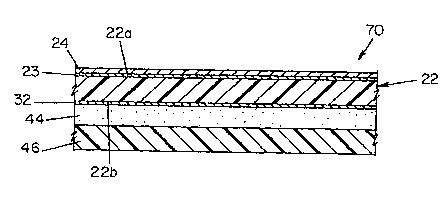
FIG. 3 shows a cross-sectional view of a flexible laminate 70 formed in
accordance with the process shown in FIG. 1, wherein a partially cured
adhesive layer
44 having a protective, removable strip 46 is attached to polymeric substrate
22 that
has a copper layer 24 on surface 22a thereof.
The foregoing description is a specific embodiment of the present invention.
It
should be appreciated that this embodiment is described for purposes of
illustration
only, and that numerous alterations and modifications may be practiced by
those
skilled in the art without departing from the spirit and scope of the
invention.
According to another aspect of the present invention, the induction heating of
web 20
may be controlled such that the temperature of the region of adhesive film 44
in
contact with the layer reaches a temperature whereby this region of adhesive
is fully
cured to a C-stage, but the outer region of adhesive film 44, and
specifically, at outer
surfaces of adhesive film does not attain a temperature for a sufficient
length of time
to fully cure such region, and therefore, the outer surface of adhesive film
remains at
least partially uncured, i.e., at an A-stage, a B-stage or a mixture of both.
It is
intended that all such modifications and alterations be included insofar as
they come
within the scope of the invention as claimed or the equivalents thereof.