Note: Descriptions are shown in the official language in which they were submitted.
CA 02332846 2000-11-20
WO 99/60683 PCT/US99/11370
BATTERY PACK PROTECTION CIRCUIT
BACKGROUND OF THE INVENTION
The present invention relates generally to portable phones and other
electronic devices employing an external battery pack to provide power, and is
particularly concerned with a protection circuit for preventing accidental
short
circuits of the exposed contacts of an external battery pack when disconnected
from the phone or charging unit.
The back of a portable phone typically has spring-loaded contacts for
mating engagement with flush contacts of an external battery pack when
releasably secured to the phone. Various types of releasable fastening devices
are used to secure such battery packs to portable phones. The battery pack
fits
into a charging unit with similar spring-loaded contacts when re-charging is
required.
One problem with such external battery packs is that they may be
accidentally short circuited by the user when not connected to the phone or
charging unit. Most such battery packs, such as Li-ion battery packs, for
example, have built in self protection circuitry for preventing overcharge or
over discharge of the battery pack. However, when spare battery packs are
carried loose in a user's bag, pocket, or purse, an accidental short circuit
may
occur where loose coins or keys connect the positive and negative exposed
contacts. Such a situation may not activate the built in self protection
circuit,
since the thresholds for such short circuits must be higher than the operating
discharge current under normal conditions, i.e. if the device draws peak
currents at 1 amp, then the self-protection circuit of the battery pack must
trip
at currents above 1 amp. This will not activate the current self protection
circuit
provided in such battery packs.
3o SUMMARY OF THE INVENTION
It is an object of the present invention to provide a new and improved
protection circuit for an external battery pack, particularly a portable phone
battery pack.
CA 02332846 2000-11-20
WO 99/60683 PCT/US99/11370
2
According to the present invention, a battery protection circuit is
provided, which comprises a switch assembly having an input for receiving a
control signal, the switch assembly controlling connection of a battery output
to
a load, a detector for detecting a resistance at a load terminal, and a
control
assembly for determining whether the resistance has a value between a
predetermined maximum value and a predetermined minimum value, and for
generating the control signal in response to the determination, the control
signal
causing the switch to close if the determination is positive, and causing the
switch to open otherwise, so that the battery output is connected to the load
only when the detected resistance has a value between the predetermined
minimum and maximum values.
Preferably, the control assembly comprises a first comparator for
comparing the resistance to the predetermined maximum value and producing
a first output signal if the resistance is above the predetermined maximum
value and a second output signal if the resistance is below the predetermined
maximum value, a second comparator for comparing the resistance to the
predetermined minimum value and for producing a third output signal if the
resistance is below the predetermined minimum value and a fourth output
signal if the resistance is above the predetermined minimum value, and a
second detector connected to the outputs of the first and second comparators
for producing the control signal to close the switch if the resistance is
between
the minimum and maximum values.
Preferably, the load to be powered by the battery has positive and
negative input contacts for connection to battery positive and negative
outputs,
respectively, and an ID output to which a predetermined load identifying
resistance is applied. When the battery is connected through the battery
protection circuit to the proper load, the ID output is connected to the first
and
second comparators which compare its resistance to the predetermined
minimum and maximum values, and only permit power to be supplied from
the battery to the load when the detected resistance is between the minimum
J
and maximum values.
In a preferred embodiment of the invention, the circuit also includes a
self-protection control unit for controlling discharge of the battery, the
control
unit having an input, an overdischarge output, and the switch assembly
CA 02332846 2000-11-20
WO 99/60683 PCT/US99/11370
3
includes a first switch controlling series connection of the battery to a load
in a
discharge mode, the first switch having a control input connected to the
overdischarge output of the control unit, and a second switch for disabling
the
first switch if the load ID resistance is detected to be outside the
predetermined
5 range between the minimum and maximum values. The second switch may be
arranged to control the power input to the control unit, so as to disable the
control unit itself when the detected resistance is outside the predetermined
range, or may be connected between the overdischarge output of the control
unit and the first switch to disable the control input to the switch in the
event
that the detected resistance is outside the predetermined range.
The control unit may also have an overcharge output, and a third switch
for controlling charging of the battery is series connected between a charge
input and a battery input, the third switch having a control input connected
to
the overcharge output. The control unit is arranged to open the third switch
15 when the battery has been charged to a predetermined value. A fourth
switch,
also controlled by the output from the second detector, may be connected
between the overcharge output and the third switch, so that the battery cannot
be charged or discharged where the detected ID resistance is outside the
predetermined range.
20 The battery protection circuit will prevent the battery from being
accidentally shorted out by metallic objects such as keys, coins or the like
when
not in use. Discharge is only possible ~n~hen the circuit detects connection
to a
load having the proper ID resistance.
25 BRIEF DESCRIPTION OF THE DRAWINGS
The present invention will be better understood from the following
detailed description of a preferred embodiment of the invention, taken in
conjunction with the accompanying drawings in which like reference numerals
30 refer to like parts and in which:
Figure 1 illustrates a battery protection circuit according to a first
embodiment of the invention;
Figure 2 illustrates a modified battery protection circuit; and
Figure 3 illustrates another modified battery protection circuit.
CA 02332846 2000-11-20
WO 99/60683 PCT/US99/11370
4
DESCRIPTION OF THE PREFERRED EMBODIMENT
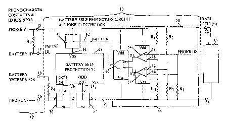
Figure 1 illustrates a battery protection circuit 10 according to a first
embodiment of the present invention connected between a load 12 such as a
5 portable phone or battery charger and the battery cell 14 of an external
battery
pack of the type normally used to power portable phones and other electronic
devices such as video game units and the like. The outer housing of the
battery
pack lzas a series of exposed contacts 15, 16, 17, 18 comprising a positive
input
terminal V-+-, a negative input terminal V-, an ID terminal, and a thermistor
10 terminal, respectively. A set of flush contacts will be provided on the
phone
and the charger unit, so that the battery pack may be releasably connected to
the portable phone or charger unit as required.
Circuit 10 includes a first connecting line 20 between V+ contact 15 and
the positive battery output 22, and a second connecting line 24 between V-
15 contact 16 and the negative battery terminal 26. In both the phone and the
charger unit, a predetermined ID resistance is provided at a phone or charger
1D terminal 17 by connecting resistor Rp between the V+ contact 15 and the
exposed ID contact 17 of the phone and charger unit. The circuit 10 is
arranged
to prevent discharge of the battery 14 unless the detected resistance is in
the
20 range between a predetermined minimum of Kp-D and a predetermined
maximum of Rp+D, where D is determined according to normal variations in
the value of the phone, charger, and battery pack resistances.
A battery temperature resistance or thermistor Rt is connected between
contact 18 and line 24. Many battery packs for portable phones, portable
25 electronics units, and the like already have a built-in self protection IC
28 and a
pair of switches 30, 32 in line 24 for controlling charging and discharging,
respectively, of the battery or cell 14, which may be an Li-ion cell or the
like.
However, in the prior art arrangements, line 20 is connected directly to the
power input 34 of the IC 28. Switches 30, 32 are preferably FETs. IC 28 has an
30 overcharge (OCD) output 36 connected to the gate of switch 30 to open the
switch and prevent any further charging if the voltage of the battery is
outside
safe limits. An overdischarge (ODD) output 38 of IC 28 is connected to the
gate
of FET 32 to open the switch and prevent discharging of the battery if the
current or voltage exceed safe limits. The nc» -mal operation of a self-
protection
35 IC of this type as normally provided in external battery packs is to allow
FETs
CA 02332846 2000-11-20
WO 99/60683 PCT/US99/I 1370
30 and 32 to enable charge and discharge of the battery pack when the current
and voltage of the battery are within safe limits, as will be understood by
those
skilled in the field.
The prior art arrangement as discussed above does not prevent
5 accidental battery discharge in the event that some metal object causes a
short
across battery pack contacts 15 and 16. The circuit in the embodiment of
Figure
1 additionally provides protection against such accidental battery discharge.
In
this embodiment, a third switch 40 is connected between power line 20 and the
power input 34. This switch is responsive to a battery enable input 42 from a
10 phone/charger identification system 44 so that the IC 28 is only switched
on
when the system 44 detects connection to a load such as a portable phone or
charger unit having an ID resistance Rp within the predetermined range, as
will
be explained in more detail below. Switch 40 is preferably also an FET.
The phone identification circuit 44 has a phone ID input 4fi ~~hich is
1_5 connected to phone ID terminal 17 at which the resistance Rp should be
present
if the battery pack is connected to a portable phone or charger input. The
phone or charger ID resistor Rp then forms a voltage divider circuit with a
resistor Rl, and the divided voltage is provided as a first input 56 to an
upper
limit comparator 50 and a first input 48 to a lower limit comparator 54. A
first
20 voltage divider circuit comprising resistors R2 and R3 sets an upper limit
voltage (Rp+D) and provides a second input 52 to upper limit comparator 50.
A second voltage divider circuit comprising resistors R4 and R5 sets a lower
limit voltage (Rp-D) and provides a second input 58 to lower limit comparator
54. The outputs RH, RL of comparators 50 and 54 are provided as inputs to an
25 OR gate circuit 60, which in turn provides the battery enable input or
control
signal 42 to the gate of FET 40.
The limits Rp +/- D are set by adjusting resistors R1 to R5 as well as Rp
in the phone and charger unit. These resistors should be set as high as
possible,
while maintaining the necessary accuracy on the maximum and minimum
30 threshold values, or excessive current will be drawn from the battery
continuously. The voltage divider circuits may alternatively be replaced with
two voltage references, but the cost of this alternative will be higher than
using
R2 R5 and the current may also be higher, depending on the reference chosen.
CA 02332846 2000-11-20
WO 99/60683 PCT/US99/I1370
6
The following logic or truth table provides the possible states of OR gate
60, where Rd is the detected resistor value at terminal 7 7:
Resistor value Rl I RL BATT. EN. COMMENTS
IZd<_IZp-D 0 1 1 Detected resistance below
low value threshold. FET
40 open, IC 28 off
Rp-D < 0 0 0 Detected resistance is in
Rd<Rp+D range. FET 40 closed and
battery pack enabled.
Rd>_Rp+D 1 0 1 Detected resistance above
high value threshold. FET
40 open, IC 28 off.
From the foregoing table, it can be seen that, unless the detected
resistance at input 46 is between the low (Rp-D) and high (Rp+D) resistance
limits, the IC 28 which controls the series charge/discharge FETs 30, 32 is
disabled. Since the IC 28 is disabled, both series FETs 30 and 32 are turned
off
and the battery cannot be discharged nor charged.
If the voltage across R1 falls between the high and low limits, the output
from OR circuit 60 will produce a voltage on the battery enable input 42 which
closes FET 40, thereby activating IC 28. This closes FETs 30 and 32, allowing
current (voltage] to appear at the external negative terminal or contact 16 of
the
battery pack.
When the battery pack is not mated to a phone or charger unit, Rp will
be infinite, and virtually no voltage will appear across R1. Thus, the voltage
on
R1 will be outside the range and IC 28 will not be activated. FETs 30 and 32
will
remain open, and no current can flow from the battery. Thus, the battery
cannot be short circuited.
The embodiment of Figure 1 may be used with any battery self
protection 1C 28 which does not have to be powered on at all times. However,
the battery pack overcharge/overdischarge protection ICs made by some a
prescribed voltage, or the IC will not function correctly after power is
restored.
The battery self-protection IC of these manufacturers has a latch which
prevents
turning on of the IC after power is restored unless a predetermined voltage is
CA 02332846 2000-11-20
WO 99/60683 PCT/US99/11370
7
seen. Thus, the circuit of Figure 1 cannot be used with self-protection 1Cs
having a built-in latch, and the circuit of Figure 2 or Figure 3 may be used
in
such cases.
Figure 2 illustrates a modified battery protection circuit 100 which may
be used with battery self protection ICs 280 which have built-in latches and
must be powered at all times. Apart from this requirement, IC 280 of Figure 2
functions in a similar manner to the IC 28 of Figure 1. A number of components
in Figure 2 are identical to those in Figure 1, and like reference numerals
have
been used for like components as appropriate.
In this embodiment, the third switch or FET 40 is located between the
ODD output 38 of IC 280 and the gate of the second FET 32. As in the previous
embodiment, a battery enable output 42 of the battery identification circuit
44 is
provided as a control input at the gate of FET 40. The logic table for this
embodiment is as follows:
Resistor value Rl-i RL BATT. EN. COMMENTS
Rd<_ Rp-D 0 1 1 Detected resistance below
low value threshold. FET
40 open, FET 32 disabled.
Discharge disabled.
Rp-D < 0 0 0 Detected resistance is in
Rd<Rp-~D range. FET 40 closed and
PET 32 enabled. Battery
-+-/- and discharge enabled.
Rd__>Rp+D 1 0 1 Detected resistance above
high value threshold. FET
40 open, FET 32 disabled.
Discharge disabled.
With this arrangement, the IC 280 is never powered down, but the
discharge FET 32 is disabled when the battery pack is not connected to
resistance Rp within the predetermined range. This approach is not as
advantageous as that of Figure 1, since the self-protection IC 280 is always
on
CA 02332846 2000-11-20
WO 99/60683 PCT/US99/11370
8
and drawing current, but it may be used in all cases where the IC must be
powered on at all times.
The embodiment of Figure 2 allows the battery pack to be charged if the
charging voltage is within safe limits, whether or not the correct ID
resistance
Rp is present, but discharge is only allowed when the battery is connected to
the phone or other predetermined load or to a charger unit. In contrast, the
embodiment of Figure 1 does not allow charge or discharge unless the detected
resistance Rp is within the predetermined range. The embodiment of Figure 2
has an advantage over that of Figure 1 in certain conditions. If an abnormal
event occurs such that the battery voltage is below normal operating range, it
is
possible to charge the battery even when the battery identification circuit is
inoperative. In this situation, it is possible to charge the cell through the
parasitic diode across the source-drain connection of FET 30.
In one specific example of a battery protection circuit as illustrated in
Figure 2, the battery self-protection IC 280 was an RM127C made by Ricoh
Corporation. Dual comparators 50, 54 were embodied in an IC 70, in this case a
MAX966EUA made by Maxim Corporation. The OR gate 60 was provided by
IC 72, in this example a TC7SL32FU made by Toshiba Corporation. These ICs
require additional resistors R6 and R7, as indicated in Figure 2. The
resistance
Rp is selected based on the nominal resistance value provided the phone. In
one particular example, Rp was nominally 130 Kohm, and D was selected to be
6°/>. However, it will be understood that other resistance values may
be used
based on the battery pack and phone to be used. In this specific example, the
following resistance values were used in the protection circuit:
R1: 150 kohm;
R2: 1.5 Mohm 01 %;
R3: 1.5 Mohm 01°/>;
R4: 1 Mohm 01 %;
R5: 1.5 Mohm 07 °/a;
R6: 510 kohm;
R7: 510 kohm;
It will be understood that the foregoing values are given by way of example
only, and that other components with equivalent functions and other nominal
CA 02332846 2000-11-20
WO 99/60683 PCT/US99/11370
resistance values may be used in order to meet the requirements of determining
if the correct ID resistance is present, within predetermined limits.
Figure 3 illustrates another modified embodiment which is functionally
more similar to that of Figure 1 but which allows a self-protection IC 280 to
be
powered on at all times. Again, like reference numerals have been used for
like
parts in this embodiment.
This embodiment is similar to that of Figure 2, with FET 40 connected between
ODD output 38 of the IC 280 and the gate of discharge FET 32. However, in this
embodiment, a fourth switch or FET 62 is connected between the OCD output
36 of IC 280 and the gate of charge FET 30. The battery enable output 42 of
the
load or phone identification circuit 44 is connected to the gates of both FETs
40
and 62, so that both the charge and discharge FETs 30 and 32 are disabled if
the
detected resistance is outside the predetermined range. The logic table for
this
embodiment is as follows:
IS
Resistor value RH RL GATT. EN. COMMENTS
Rd ( Rp-D 0 1 7 Detected resistance below
low value threshold. FETs
40 and 62 open, discharge
and charge disabled.
Rp-D < 0 0 0
Rd<Rp+D Detected resistance is in
range. FETs 40 and 62
closed and battery pack
Rd>_Rp+D 1 0 1 Detected resistance above
high value threshold. FETs
40 and 62 open, pack
discharge and charge
disabled.
The embodiment of Figure 3, like that of Figure 1, shuts off both the
charge FET 30 and the discharge FET 32 when the detected resistance Rp is
outside predetermined limits. If resistance Rp is within predetermined limits,
the ODD and OCD output pins of IC 280 operate in the normal mannerto
CA 02332846 2000-11-20
WO 99/60683 PCT/US99/11370
enable discharge and charge of the battery pack when the current and voltage
of the battery are within safe limits.
In each of the above embodiments, in addition to providing normal
discharge and charge controls based on the current, voltage, and temperature
of
5 the battery pack, the protection circuit will additionally permit battery
discharge only when the battery pack is detected to be connected to an output
load such as a portable phone or charger unit having an ID resistance Rp
within
a predetermined range. This prevents any discharge of the battery as a result
of
an accidental short circuit across battery contacts 75 and 16. If the circuit
is
10 open and no load is connected, the detected resistance Rd will be infinite,
i.e.
above the predetermined maximum value. If a short circuit occurs, the detected
resistance will be zero, i.e. below the predetermined minimum value. Thus,
discharge can only occur when the battery pack is mated to the portable phone,
charger unit, or other electronic device with which it is intended to be used.
It will be noted that each of the FETs in Figures 1 to 3 have a parasitic
diode connected across the source-drain connection. FETs 40 and 62 may be
replaced by PNI' transistors or other electronic switching devices, but the p-
channel FET as illustrated in the drawings provides the lowest voltage drop
for
this application and is preferred. Similarly, FETs 30 and 32 may be replaced
by
other electronic switching devices, although n-charmel FETs are preferable
since
they also provide the lowest possible voltage drop.
With the above protection circuits, it will still be possible for a
phone/charger to differentiate between a broken battery pack and no battery
pack connected. When a battery pack is connected, the ID voltage will equal:
R1/(R1+Rp)'~(V+ - V-)
under normal conditions, and will be undefined if no external battery is
present or if the protection circuit is disabling the battery pack connection
(i.e.
if it is broken). The phone/charger may be arranged to measure the resistance
between the V- pin and the thermistor terminal 18 directly connected to the
pack, or indirectly by creating a voltage divider to a fixed voltage
reference.
The phone/charger can then differentiate between a broken external battery
pack protection circuit and no battery connected according to the following
logic or truth table:
CA 02332846 2000-11-20
WO 99/60683 PCT/US99/I 1370
Battery ID pin voltageBattery TEMP Battery State to
Resistance Phone/Charger
Valid Range Valid Range Connected and functional
Valid Range Invalid Range Connected and out
of
operating temp /
range
Invalid Range Valid Range Connected and non-
functional if steady
state.
Tnvalid Range Invalid Range No battery connected.
IO The battery pack protection circuits described above therefore prevent
accidental short circuit of exposed battery pack contacts, for example when a
battery pack is carried loose in a purse, bag, or pocket while not in use. The
circuit does not allow the exposed battery contacts on the pack to be active
until
it is determined that the pack is mated to the phone or charger unit.
Although a preferred embodiment of the invention has been described above
by way of example only, it will be understood by those skilled in the field
that
modifications may be made to the disclosed embodiment without departing
from the scope of the invention, which is defined by the appended claims.
I CLAIM: