Note: Descriptions are shown in the official language in which they were submitted.
CA 02333333 2001-01-31
1 P/70046.CAP/HV
IMPROVEMENTS IN ELECTRICAL PROTECTION AND CONTROL SYSTEMS
Field of the Invention
This invention relates to improvements in protection and control systems for
use in
power generation, transmission and distribution, and in particular to an
improved
design of status acquisition apparatus for monitoring the status of devices
forming
part of such systems, e.g., relays, circuit breakers, interrupters, isolators
and
similar protective switching devices.
Background of the Invention
It is well known, for example, that a protective relay includes appropriate
circuitry
that monitors the condition of a power system circuit in order to decide when
to
trip the circuit breaker of that circuit. The output contact of the protective
relay
can either be used for driving the trip coil of the circuit breaker directly,
or can be
used to signal another protective relay, via a status acquisition apparatus
associated
with that relay, that it has detected an event. The circuit connecting the
output
contacts of the protective relay (or any other external apparatus) to the
status
acquisition apparatus of another protective relay is known as a status
circuit. The
status circuits require an external power supply for them to operate.
The protection relay circuitry is driven by a power supply that is independent
of
the electrical circuit that is being protected. In many cases the protection
relays
will be powered from an independent battery supply. This is usually 24/27V,
30/34V, 48/54V, 110/125V or 220/250 volts depending on the type of
installation.
This supply will also be used to power the status circuits. More than one
battery
voltage may be present in any given installation.
Protective relays are usually housed in non-ventilated enclosures to improve
reliability. Low power dissipation of any electrical circuitry provided in the
enclosure is therefore essential.
CA 02333333 2001-01-31
2 P/70046.CAP/HV
A protective relay will typically incorporate status acquisition apparatus
which
allows interaction between a number of protective relays and other associated
external apparatus. The status acquisition apparatus may be an integral part
of the
protection relay circuitry located within the non-ventilated enclosure.
The signals fed into the status acquisition apparatus will be used by the
protective
relay, in conjunction with data obtained from its own monitoring circuitry, to
determine when to initiate a trip via its output contacts. The status
acquisition
apparatus has two defined states: One state indicates `valid signal' where the
voltage present at its input is above a defined threshold and the other
indicates `no
signal' where no voltage or a voltage less than the threshold is present.
Of course, a status acquisition apparatus may be adapted to monitor the status
of
the output of other devices as well as or instead of relays. They may be
incorporated in a variety of systems for control or monitoring or any other
application where fault monitoring or general status monitoring is needed.
The status acquisition apparatus design must meet several criteria. It must
tolerate
noise on the battery voltage without producing a false signal yet provide a
rapid
response if a true signal is detected. It must consume a minimum amount of
power
if it is located within a sealed housing and ideally be easily reconfigured to
operate
with different battery voltages.
Several prior-art status acquisition apparatus designs have been developed
which
can cope with a range of different supply voltage ratings. In one arrangement
it is
known to provide a constant current circuit which is fed from the battery
voltage.
The circuit draws a constant current from the battery supply that is used to
drive an
opto-isolator. The opto-isolator produces a `valid signal' output as long as
the
current drawn exceeds the turn-on threshold of the opto-isolator. This depends
on
CA 02333333 2010-03-12
'30811-11
3
the current transfer ratio of the opto-isolator. If the battery voltage is not
present
or drops too low then the circuit cannot draw current, the opto-isolator
produces no
output, indicating that no signal is present.
A problem with the use of the constant current circuit is that the circuit
will
consume more power at a higher supply voltage than at lower supply voltage
(since
power = current multiplied by voltage). Thus, a constant current based circuit
that
is sufficiently sensitive to operate at the lowest expected battery voltage
(say 24/27
volts) will have excessive power dissipation at the largest expected input
voltage
(say 220/250 volts).
In an alternative design, it has been proposed periodically to sample the
input
voltage for a fixed period. Current is able to flow through the opto-isolator
for the
duration of the sampling interval. Appropriately valued linear components,
such as
resistors and capacitors, are used in the circuit to set the current level, By
getting
a customer to specify the battery voltage of their system, a variant of the
circuit
using the most suitable linear components can be offered to meet their
requirements. In this way power drawn is kept to a minimum. Unfortunately,
this
limits the use of the circuit to specific supply voltages, and if the
incorrect variant
of the circuit is used then it may be damaged.
It is an object of the present invention to overcome at least partially the
disadvantages present in prior art systems.
Summary of the Invention
In accordance with a first aspect the invention provides a protection and
control
system for use in power generation, transmission and distribution, the system
including status acquisition apparatus for monitoring the status of at least
one device in the system; the apparatus comprising:
CA 02333333 2001-01-31
4 P/70046.CAP/HV
conversion means adapted to receive an input signal representative of the
status of the device and convert the input signal into a pulse width modulated
signal, the mark-space ratio of the pulse width modulated signal decreasing
with
the magnitude of the input signal, and
comparison means adapted to compare the mark-space ratio of the pulse
width modulated signal with a reference value and produce a status indication
signal in the event that the result of the comparison meets a predetermined
criterion.
The invention thus provides apparatus in which the input signal is converted
to a
pulse width modulated waveform which changes in mark-space ratio as the input
voltage increases. By making the mark-space ratio decrease for increases in
the
magnitude of the input signal, such as an increasing input voltage, it is
possible to
ensure that at low voltages the power dissipated is similar to that dissipated
at high
voltages.
The pulse width modulated signal may comprise a single on-period (mark) and a
single off-period (space) within each cycle. Of course, other pulse width
modulated
waveforms are envisaged.
The device that produces the status signal may comprise any device, apparatus
or
circuit from which a signal indicative of an event such as the status of a
switch or
of a voltage level can be obtained. This may in one application comprise a
protection relay with the status signal comprising a signal representative of
the
switching state of the relay. The status signal may therefore be indicative of
the
status of the relay contact, i.e. open or closed.
Alternatively, it is envisaged that the input to the status acquisition
circuit may be
a signal taken from alternative devices. It may, for example, be a voltage
taken
from a point in a circuit to be monitored. It may be a direct or indirect
measure of
CA 02333333 2001-01-31
P/70046.CAP/HV
a battery voltage, for example of a supply battery associated with a relay or
other
device. In this case the status acquisition apparatus would monitor the
battery
voltage.
5 The input signal to the status acquisition apparatus will typically comprise
a DC
voltage. Alternatively, it may comprise an alternating voltage. In the later
case, the
conversion means may be associated with a rectifier that converts the
alternating
voltage to a DC voltage signal prior to inputting it to the conversion means.
In
both cases, the mark-space ratio of the pulse width modulated waveform will
decrease with increasing voltage magnitude.
Preferably the apparatus includes means for providing a user-definable pre-set
reference value to the comparison means. Thus, it is possible simply to adapt
the
apparatus to different input voltages by changing the reference value. No
physical
components need be changed, so the apparatus can be readily adapted to monitor
the status of a wide range of devices by choosing the appropriate reference
for the
signal that is being monitored. This is conveniently achieved by storing the
reference value in a memory, the memory being accessed by the comparison means
to read the preset reference value. The memory may be an electronic memory
such
as static or dynamic random access memory.
The apparatus may further include an opto-isolator which is adapted to
electrically
isolate the input signal applied to the comparison means from the conversion
means.
The apparatus may include means for generating an internal, low voltage supply
from the battery supply connected to the input to the conversion means. This
may
include a voltage regulator and may provide a supply for the comparison means.
CA 02333333 2001-01-31
6 P/70046.CAP/HV
The conversion means may comprise timer circuit means adapted to output the
pulse width modulated signal. The timer circuit means may include an astable
first
timer/oscillator circuit which generates a periodic control signal, for
example a
pulsed waveform, that provides a trigger for a monostable second
timer/oscillator
circuit to output the pulse width modulated signal.
The conversion means may further include in electrical series a switching
means, a
resistor and a capacitor the switching means being connected to receive the
input
signal, whereby when the switching means is closed the capacitor charges at a
rate
dependent upon the magnitude of the input signal (and the component values),
opening and closing of the switching means being controlled by the output of
the
second timer/oscillator circuit. A second switching means may be included that
is
connected across the capacitor, the capacitor discharging through the second
switching means when it is closed and not discharging when the second
switching
means is open, thereby allowing the capacitor to be charged through the first
switching means, opening and closing of the second switching means also being
controlled by the output of the second timer/oscillator circuit. The two
switching
means operate in opposing sense i.e. when one is open the other is closed.
The capacitor may be provided with a monitoring means for outputting a measure
of the charging voltage across the capacitor to the second timer/oscillator
circuit,
the second timer/oscillator circuit being provided with threshold means such
that
the status signal output of the second timer/oscillator is negated when the
voltage
across the capacitor reaches a threshold value.
The pulse-width modulated signal output of the second timer/oscillator circuit
may
provide an input to the opto-isolator whereby the isolator outputs a pulse
width
modulated output signal to the comparison means. The output of the opto-
isolator
will be asserted when the output of the second timer/oscillator circuit
exceeds the
isolating turn-on voltage, and be negated when it is below this.
CA 02333333 2010-03-12
'30811-11
7
The comparison means may include a counter, and means enabling the
counter to be incremented by a clock signal in dependence on the state of the
pulse width modulated signal. The count signal may be updated periodically,
e.g.
every millisecond.
Means may be provided for enabling the counter to be incremented by a clock
signal only while the pulse width modulated signal is high.
Alternatively, the counter may be incremented by a clock signal for the
duration of each mark-space ratio pair of the pulse width modulated signal. In
either case, means are provided to reset the counter to a start value, such as
zero, at
the end of every mark-space ratio pair, of the pulse width modulated signal.
The comparison means may be adapted to compare the pulse width modulated
signal with the reference value by comparing an output of the counter at the
end of a pulse of the pulse width modulated signal with the reference value.
The
comparison means may be adapted to produce the status indication signal if the
output of the counter exceeds the reference value, such exceeding of the
reference value being the predetermined criterion. This will indicate the
pulse is
too long and hence voltage at the input of the status acquisition apparatus is
too
low (i.e. mark-space ratio too high).
Alternatively, the comparison means may be adapted to compare the state of the
pulse width modulated signal with an expected state when the output of the
counter
has reached a value determined by the reference value, said expected state
being the predetermined criterion. _ For example, if the pulse has not
finished once
the count has reached a reference value this may be used to indicate the
voltage at
the input of the status acquisition apparatus is too low.
CA 02333333 2010-03-12
'30811-11
8
In a further refinement, means may be provided for translating the output of
the
counter at the end of a pulse of the pulse width modulated signal into a
digital word representative of the actual voltage at the input of the status
acquisition apparatus.
It will be readily appreciated that by providing a different reference value
the
apparatus can be easily adapted to different battery voltages. There is no
need to
change electrical component value, and the power dissipation can be optimised.
In accordance with a second aspect, the invention provides a protection and
control
system according to any preceding claim, in which the status acquisition
apparatus
is part of a protective switching device whose status is being monitored.
The protective switching device may be housed within a non-ventilated
enclosure.
The output from the status acquisition apparatus may be fed to an indicator
such as
a bulb or perhaps to a microprocessor. It may be fed by a microprocessor
together
with the output of other status acquisition apparatus for subsequent
processing.
The battery may have a nominal voltage of substantially more, than 24 volts or
less
that 250 volts and an absolute voltage of substantially more than 16.2 volts
or less
that 300 volts
CA 02333333 2010-03-12
'30811-11
8a
In accordance with another aspect, there is provided a protection
and control system for use in power generation, transmission and distribution,
the
system including status acquisition apparatus connected to monitor the status
of
at least one device in the system; the apparatus comprising: conversion means
adapted to receive an input signal having a variable magnitude and
representative
of the status of the device and convert the input signal into a pulse width
modulated signal having a mark-space ratio which is inversely proportional to
the
magnitude of the input signal, and comparison means adapted to compare the
mark-space ratio of the pulse width modulated signal with a reference value
and
produce a status indication signal in the event that the result of the
comparison
meets a predetermined criterion.
In accordance with a further aspect, there is provided a protection
and control system for use in power generation, transmission and distribution,
the
system including status acquisition apparatus connected to monitor the status
of a
protective relay in the system, the apparatus comprising: conversion means for
receiving an input voltage representative of the status of the device and for
converting the input voltage into a pulse width modulated signal having a mark-
space ratio which decreases as the input voltage increases to maintain power
dissipation below a predetermined power; and comparison means for comparing
the marked-space ratio of the pulse width modulated signal with a reference
value,
and for producing a status indication signal in the event that a result of a
comparison meets a predetermined criterion.
Brief Description of the Drawings
There will now be described, by way of example only, one
embodiment of the present invention with reference to the accompanying
drawings of which:
Figure 1 illustrates a protection scheme including .a protection relay
with a status acquisition apparatus in accordance with the present invention;
CA 02333333 2001-01-31
9 P/70046.CAP/HV
Figure 2 is a schematic illustration of the main elements of the status
acquisition apparatus;
Figure 3 is an illustration of the circuit elements that make up the
conversion circuit of the status acquisition apparatus;
Figure 4 is a graph showing the waveforms generated at various points of
the conversion circuit when in use;
Figure 5 is a schematic showing the various functional elements of the
comparison circuit of the status acquisition apparatus; and
Figure 6 is a graph showing output voltage waveforms within the
comparison circuit and demonstrating the way in which the signal is
processed to determine the voltage status.
Detailed Description of the Preferred Embodiments
As illustrated in Figure 1 of the accompanying drawings, a typical protection
scheme for protecting a section of line 1 or piece of equipment comprises of a
number of protection relays 2,3 and other pieces 4 of external monitoring and
control equipment. One or more circuit breakers will be placed in series with
the
item to be protected to control the current flow. Hence, as shown, the
operation of
a circuit breaker(s) is controlled by output 5 from the first protection relay
2 to a
trip circuit 6.
The protection scheme will generally be powered from a battery supply 8 to
provide maximum security of the supply.
Typically, as illustrated in Figure 1, a status acquisition apparatus 100 is
used
when one protective relay 3 (or any other external apparatus 4) is required to
CA 02333333 2001-01-31
P/70046.CAP/HV
modify the operation of another protective relay 2 instead of directly
tripping a
circuit breaker. In the illustrated embodiment, the output 9 from the contacts
10 of
one of the protective relays 3 is used to switch an auxiliary battery supply
onto the
status acquisition apparatus 100 of the other protective relay 2. The
protective
5 relay 2 can then use this additional information in conjunction with data
obtained
from its own monitoring circuitry 16, to determine what action to take. Output
contacts 12 of the protective relay 2 may then be used to operate visible or
audible
warning devices (not shown), and/or initiate a trip of the breaker. If the
device has
remote communications facilities then the signal may be passed along a
10 communications line to a central monitoring station.
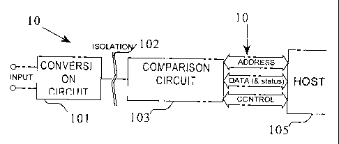
The status acquisition apparatus 100 is illustrated schematically in Figure 2
of the
accompanying drawings.
The status acquisition apparatus 100 comprises two main circuits. Firstly, an
input
signal (in this case the DC voltage from the battery or the status output of
the
second relay 3) is fed to an input or conversion circuit 101. As shown, this
is via a
direct connection to the battery, but it could be fed through a bridge
rectifier to
allow status acquisition using AC voltages. The conversion circuit 101
incorporates means to generate a pulse-width modulated signal in which the
pulse-
width is dependent upon the magnitude of the signal input to the conversion
circuit
101.
The pulse width modulated signal is then passed through an opto-isolator 102
to a
measurement or comparison circuit 103 which generates a status indication
output
signal 104 dependant upon the pulse width of the output of the opto-isolator.
In
the embodiment shown, the status output is high where the voltage present at
its
input is above a defined threshold and low where no voltage or a voltage less
than
the threshold is present. This status signal 104 will then be converted into
appropriate signals that can be read by the relay's host microprocessor 105
through
CA 02333333 2001-01-31
11 P/70046.CAP/HV
the bus interface. It is envisaged that other forms of digital output may be
produced.
The conversion circuit 101 is illustrated in more detail in Figure 3 of the
accompanying drawings and consists of two timer/oscillator circuits 111, 112,
both
being 555 timer integrated circuits, the first of which is configured as an
astable
oscillator. This produces a pulsed output waveform of fixed frequency and duty
cycle. The pulsed waveform provides a trigger signal for the second timer
circuit
112, enabling the second timer circuit 112 to produce the pulse width
modulated
signal from the input voltage applied to the input circuit.
Meanwhile, the output 113 of the second timer circuit 112 is connected to a
constant current source consisting of an N-channel FET and a sensing
resistor(not
shown). The constant current source is used to drive the base of a switching
transistor 105. One side (the emitter) of the transistor 105 is connected
directly to
the input voltage Vin whilst the other is connected via a resistor 106 to one
side of
a capacitor 107. The other side of the capacitor 107 is connected to the
common
earth point of the conversion circuit 101.
When the input waveform applied to the trigger input of the second timer
circuit
112 switches from low to high the transistor is switched on which allows
current to
flow from the input to charge the capacitor 107. The resistor 106, connected
in
series with the capacitor 107 and the transistor 105, limits the rate at which
charge
builds up onto the capacitor.
Whilst the transistor remains turned on (i.e. the output of the first timer
circuit 111
remains high) the capacitor 107 will continue to charge. The rate at which it
charges is dependent upon the magnitude of the input voltage signal.
CA 02333333 2001-01-31
12 P/70046.CAP/HV
A voltage divider 108 is connected across the capacitor 107and a proportion of
the
voltage across the capacitor 107 is fed from a tap 109 on divider 108 to the
threshold input of the second timer circuit 112. Thus, as soon as the voltage
across
the capacitor 107 reaches a pre-determined threshold level the output of the
second
timer circuit 112 will go low. This turns off the switching transistor 105 and
at the
same time, the capacitor is discharged by a transistor switch (not shown)
which is
integrated into the timer circuit 112. The switching transistor 105 remains
off and
the capacitor 107 remains discharged until the trigger input of the second
timer
circuit 1 1 2 receives a subsequent pulse from the first timer circuit 1 1 1.
The opto-isolator 102 is also connected to the output 113 of the second timer
circuit 112. This opto-isolator 102 comprises a diode which illuminates a
phototransistor when energised. As long as the switching transistor 105 is
switched
on the opto-isolator 102 is energised. When the transistor 105 is switched off
the
opto-isolator is de-energised. The output from the opto-isolator 102 comprises
a
digital pulse width modulated signal. The pulse width of the opto-isolator
output
is dependent on the input voltage as a result of the operation of the
conversion
circuit.
The two timer circuits are powered by a voltage supply Vaux that is generated
from the input voltage Vin. This is by way of an N channel FET that produces a
roughly regulated output of nominally 10 volts. The rough voltage is fed to a
series regulator to provide a smooth 5 volt supply Vreg. A rectifier diode
ensures
that the input to the whole circuit is polarised.
Overall protection for the circuit is provided by a Metal Oxide Varistor (MOV)
110 connected across the input terminals.
The di-electric of the timing capacitor 107 which is repeatedly charged and
discharged is selected to have a stable value over a range of temperatures
which
CA 02333333 2001-01-31
13 P/70046.CAP/HV
are compatible with the operational environment of the circuit. For example, a
class 1 multi-layer ceramic capacitor with a COG (NPO) di-electric. This type
of
capacitor is temperature compensating and in general does not have an ageing
characteristic. The resistor value in series with the capacitor is chosen to
allow
adequate time for the timer circuit 112 to discharge the capacitor and for the
circuit to settle at all expected input voltages.
Because the charging current to the capacitor 107 is switched off as soon as
the
threshold voltage is reached (by turning off the switching transistor 105) the
power
dissipated by the circuit is minimised.
In practice, the switching transistor 105 is comprised of an HV (high voltage)
type
transistor which is driven from the previously mentioned constant current
source
consisting of an HV N-channel FET and a sensing resistor driven from the
output
of the second 555 timer.
The opto-isolator provides isolation in excess of 2.5kV rms. between the
conversion circuit and the comparison circuit. Obviously, this could be
increased
or lowered depending on the operational requirements and degree of protection
needed.
The output 114 of the input circuit 101 is an encoding of the input voltage
Vin, in
the form of a digital pulse width modulated signal. This is fed to the
measurement
circuit 103(Figure 2). The waveforms describing operation of the input circuit
are
shown in Figure 4 of the accompanying drawings.
As schematically shown in the block diagram of Figure 5, the measurement
circuit
103 is implemented in hardware using programmable logic. Each comparison
circuit 103 needs an input 114 to receive the modulated signal from the input
circuit 101 and an output 104 to provide the status signal. Control inputs 200
are
CA 02333333 2001-01-31
14 P/70046.CAP/HV
provided for selection of one of a set of preset reference (comparison)
constants
201 and a clock signal 202 is also provided to drive a counter 203. One likely
use
of the status acquisition apparatus would be as part of a microprocessor based
protective relay in a power system and in this case the measurement circuit
would
be connected to the microprocessor bus via a bus interface circuit.
The comparison circuit 103 comprises a counter 203 that is triggered through
clock
synchronisation circuit 204 when the waveform 114 from the input circuit 101
is
asserted, i.e. goes high; this is a mark rather than a space. The counter 203
then
increases for as long as the pulse remains asserted. It is reset to zero and
re-
triggered on the arrival of the next pulse.
A comparator circuit 205 is provided which compares the value held in the
counter
203 with the selected reference value 201. Five reference values have been
implemented that can be selected by three of the control lines 200.
For example, in the case of a power system protective relay, the control lines
200
are driven by the microprocessor associated with the relay. This allows the
appropriate setting to be selected through the user interface of the
protective relay.
Once the value output from the counter 203 has reached the pre-set reference
value
a check signal is sent to a status register 206. The register then immediately
measures the status of the pulse supplied from the input circuit. This is
illustrated
by the graphs in Figure 6 of the accompanying drawings. The top graph shows
that
if the pulse waveform is still asserted when the comparison is made, then the
output of the status register 206 is set to `no signal'(Status = off). The
bottom
graph of Figure 6 shows that if the pulse waveform is negated when the
comparison is made, then the output of the status register 206 is set to
`valid
signal'(Status = on).
CA 02333333 2001-01-31
15 P/70046.CAP/HV
In a modification, the counter 203 may instead continue to count until the
pulse
from the opto-isolator is negated. The counter value is then compared with the
pre-set reference value to check the status of the input voltage and produce
an
appropriate output status. Alternatively, the counter value when the pulse
from the
opto-isolator is negated is recorded and translated into a digital word that
represent
the actual voltage on the input.
In practice, we have found that the status acquisition apparatus constituted
as
described is capable of measuring a wide voltage range (12-300 volts) at a
current
of more than 3 milliamps while maintaining a power dissipation of less than
0.2
Watts. This is achieved because the input voltage is converted into a pulse
waveform whose width decreases as the input voltage increases, the widths of
the
pulses being compared to fixed reference values to provide the apparatus with
an
on/off output status. Hence, the circuits are switched on for shorter periods
at
higher voltages, giving the desired reduced power dissipation.