Note: Descriptions are shown in the official language in which they were submitted.
CA 02333775 2001-O1-09
1
PRECISION-CONTROLLED DUTY CYCLE CLOCK CIRCUIT
BACKGROUND OF THE INVENTION
1. Field of the Invention
The invention relates to the field of precision-controlled duty cycle clock
circuits for use with electronic devices. More specifically, the invention
provides
a circuit having an adaptive adjustment to improve the controllability of the
duty
cycle of an output clock signal in response to the changing characteristics of
an
input clock signal. The invention finds application in a variety of electronic
devices, including wireless communications devices.
2. Description of the Related Art
Many high performance clocked digital circuits require a clock signal
with a precisely controlled duty cycle. These types of circuits may use both
the
high and low phases of the clock signal to perform computations. If, for
example,
a circuit has the same timing requirements for both the high and low phase of
the
clock signal, then a clock signal with an accurate 50/50 duty cycle yields the
maximum amount of time in each phase of the clock signal for any given
1 S frequency. Clock sources with less accurate control over their duty cycle
would
have to operate at a lower frequency to meet the timing requirements of such a
circuit. Hence, clock circuits providing accurate duty cycle control allow
either
a higher clock rate or a lower core voltage, while still maintaining adequate
timing margin for circuits operating from both phases of the clock signal.
464012v1
CA 02333775 2003-O1-22
SUMMARY OF THE INVENTION
2
A clock signal duty cycle control circuit is provided that receives an
incoming
signal from a clock signal input source and generates an improved output clock
signal
having an accurately controlled duty cycle. The circuit controls the duty
cycle of the
output clock signal by comparing the incoming signal to a reference value with
a
comparator. The reference value is derived from a reference charge stored on a
capacitor. The reference charge is built up in the capacitor using the
currents from a
current source and a current sink, which are controlled using translated
output signals
from the comparator.
The duty cycle may be controlled by a reference value generated by building
up of charge on a capacitor with a reference current. The charge, which is
based on
the reference current produced by combining currents flowing from a current
sink and
current source, produces a voltage across the capacitor. The current source
and sink
include devices that are programmed during a precharge mode of operation.
During
programming, the devices memorize a predetermined solution such that during a
normal mode of operation the source current is identical to the sink current.
Various aspects of the invention are defined as follows:
An apparatus comprising:
a clock source configured to generate a first clock signal having an undefined
duty cycle;
a clock signal duty cycle controller coupled to the clock source and
configured
to process the first clock signal and output a second clock signal having a
precisely
controlled duty cycle; and
CA 02333775 2003-O1-22
2a
a clock signal utilizing device operatively coupled to the clock signal duty
cycle
controller, wherein the clock signal duty cycle controller includes a circuit
configured
to generate the second clock signal, the circuit comprising:
a comparator;
a signal processing device coupled to an output terminal of the comparator and
operable to generate control signals;
first and second current devices coupled to the signal processing device to
receive the control signals; and
a reference charge storage device operatively coupled between the first and
second current devices and the comparator.
A clock signal duty cycle controller, comprising:
a comparator configured to receive an input clock signal and a reference
signal, and to output a precision controlled duty cycle clock signal;
a signal processing device coupled to the output of the comparator;
first and second current devices coupled to the signal processing device; and
a reference charge storage device for generating a reference signal
operatively
coupled between the first and second current sources and the comparator.
An apparatus configured to convert a curvilinear clock signal into a square-
wave clock signal and to program current, comprising:
a voltage controlled current source, the current source including a pFET
coupled to first, second, and third source switches and a source capacitor;
and
a voltage controlled current sink, the current sink including a nFET
coupled to the pFET and coupled to first, second and third sink switches and a
sink
capacitor.
CA 02333775 2003-O1-22
2b
A clock signal duty cycle controlling apparatus, comprising:
means for generating a clock signal;
means for receiving the clock signal, the means for receiving being configured
to generate an output clock signal with a predetermined duty cycle based on
the
received clock signal; and
means for propagating logic based on the output clock signal.
A method comprising the steps of
receiving a clock signal with an undefined duty cycle;
generating an output clock signal with a predetermined duty cycle by: (A)
comparing the received clock signal to a reference value in order to generate
the
output clock signal; (B) translating the output clock signal to generate a
plurality of
second signals based on the output clock signal; (C) utilising the plurality
of second
signals to control first and second current devices that generate the
reference value.
An apparatus comprising:
a clock source configured to generate a first clock signal having an undefined
duty cycle;
a clock signal duty cycle controller coupled to the clock source and
configured
to process the first clock signal and output a second clock signal having a
precisely
controlled duty cycle;
a clock signal utilizing device operatively coupled to the clock signal duty
cycle controller;
wherein the clock signal duty cycle controller includes a circuit configured
to
generate the second clock signal, the circuit comprising:
a comparator;
CA 02333775 2003-O1-22
2c
a signal processing device coupled to the comparator;
first and second current devices coupled to the signal
processing device; and
a reference charge storage device operatively coupled between the first
and second current devices and the comparator; and wherein
the reference charge storage device is coupled to a negative terminal of the
comparator;
the clock source is coupled to the positive terminal of the comparator; and
the clock signal utilizing device is coupled to an output terminal of the
comparator.
An apparatus comprising:
a clock source configured to generate a first clock signal having an undefined
duty cycle;
a clock signal duty cycle controller coupled to the clock source and
configured
to process the first clock signal and output a second clock signal having a
precisely
controlled duty cycle;
wherein the clock signal duty cycle controller includes a circuit configured
to
generate the second clock signal, the circuit comprising:
a comparator operable to output at an output terminal the second clock
signal having the precisely controlled duty cycle;
a signal processing device coupled to the output terminal of the
comparator and operable to generate control signals;
CA 02333775 2003-O1-22
2d
a current device coupled to the signal processing device and operable
to control a current in response to the control signals generated by the
signal
processing device; and
a reference charge storage device operatively coupled to the current
device and operable to store a charge in response to the current controlled by
the
current device.
The invention is described in more detail below in terms of a preferred
embodiment. As will be appreciated, the invention is capable of other and
different
embodiments, and its several details are capable of modifications in various
respects,
all without departing from the invention. Accordingly, the drawings and
description
of the preferred embodiments are to be regarded as illustrative in nature and
not
restrictive.
CA 02333775 2001-O1-09
3
BRIEF DESCRIPTION OF THE DRAWINGS
The present invention will be apparent to those skilled in the art upon
reading the following description in view of the accompanying drawings,
wherein:
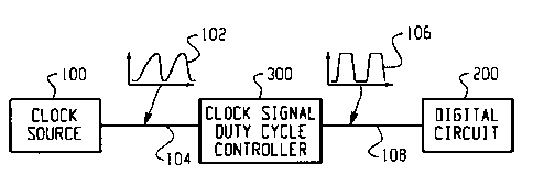
FIG. 1 is a block diagram of a clock signal duty cycle controller coupled
between an input clock source and a clocked digital circuit;
FIG. 2 illustrates a preferred output clock signal generated by the clock
signal duty cycle controller of FIG. 1;
FIG. 3 illustrates several cycles of an input clock signal to the clock signal
duty cycle controller and an output clock signal from the clock signal duty
cycle
controller;
FIG. 4 is a schematic diagram of a preferred clock signal duty cycle
controller as shown in FIG. l;
FIG. 5 is a schematic diagram showing the current source and current sink
section of the clock signal duty cycle controller of FIG. 4;
FIG. 6A illustrates a waveform representing a voltage input to the clock
signal duty cycle controller shown in FIG. 4;
FIG. 6B illustrates a waveform representing a voltage output from the
clock signal duty cycle controller shown in FIG. 4;
FIG. 6C illustrates waveforms that represent the capacitor currents
flowing from a current source and a current sink shown in Figs. 4 and 5;
FIG. 6D illustrates a waveform that represents a change in charge on a
reference capacitor in the clock signal duty cycle controller shown in Figs. 4
and
464012v1
CA 02333775 2001-O1-09
4
5;
FIG. 7 is a circuit architecture of the current source and the current sink
shown in FIG. 4 during a precharge mode of operation; and,
FIG. 8 is a circuit architecture of the current source and current sink
S shown in FIG. 4 during a source/sinking mode of operation.
DETAILED DESCRIPTION OF THE DRAWINGS
Turning now to the drawing figures, FIG. 1 sets forth a block diagram of
a clock signal duty cycle controller 300 coupled between an input clock source
100 and a clocked digital circuit 200. As shown in this figure, the input
clock
source 100 transmits a first clock signal 102, preferably a curvilinear
signal, to
a clock signal utilizing device 200, preferably a clocked digital circuit, via
the
clock signal duty cycle controller 300. The first clock signal 102 generated
by
the clock source 100 and placed on path 104 may be poorly conditioned due to
1 S unknown DC offsets, unknown amplitudes or an asymmetrical waveform. In
contrast, a second clock signal 106 output from the clock signal duty cycle
controller 300, preferably a square-wave clock signal, has an accurately
controlled duty cycle and adjusts to changes in characteristics of the clock
source
100. The second clock signal 106 is placed on path 108 to be used as the
clocking signal for the clocked digital circuit 200.
FIG. 2 illustrates a preferred output clock signal 106 generated by the
clock signal duty cycle controller 300. In one clock period (t~e,;od), the
clock
signal 106 includes a high phase signal component (measured in time by tH), a
464012v1
CA 02333775 2001-O1-09
low phase signal component (measured in time by tL), and an uncertainty
component (measured in time by tX.) Preferably, the clocked digital circuit
200
performs logic processes during both the high phase (tH ) 110 and the low
phase
(tL) 112 of the clock signal 106. Minimizing the uncertainty phase (tX) 114
S permits optimization of the duty cycle (tH / tL) of the clock signal 106.
By maximizing tH and t~, the digital circuit 200 can operate at higher
clock speeds, it can operate at a lower supply voltage, it can operate at
extreme
temperatures, or some combination of these parameters. The clock speed, supply
voltage, and temperature determine the propagation delay of the digital
circuit
200.
When designing a clocked logic circuit, a circuit designer must assume
the worst case scenario for the propagation delay of the circuit. This
assumption
is based on the maximum amount of time the clock signal needs to spend in
either
it's high or low phases, and the minimum amount of time that is guaranteed to
be
present in the associated portion of the clock signal. Accordingly, to
accommodate the propagation delay it is desirable to minimize the uncertainty
component (tX) in the clock signal. By doing so, the high.and low phases 110,
112 of the clock signal 106 can be used with maximum efficiency.
For example, the clock signal 106 might have a duty cycle (tH / tL)
between 40/60 and 50/50, e.g., 40 ns/60 ns and SO ns/SO ns. In this case, the
high
phase of the clock signal (tH) could be anything between 40 ns and 50 ns,
which
results in 10 ns in the uncertainty phase (tX) 114. This time in the
uncertainty
phase 114 cannot be relied upon when determining worst case scenarios. Hence,
464012v1
CA 02333775 2001-O1-09
6
a digital circuit 200 must be designed that propagates logic in 40 ns. If the
time
in the uncertainty phase 114 is reduced to 1 ns, then the digital circuit 200
can be
designed to propagate signals in 49 ns, thus permitting a greater degree of
freedom for the circuit designer.
FIG. 3 illustrates several cycles of an input clock signal 102 to the clock
signal duty cycle controller 300 and an output clock signal 106 from the clock
signal duty cycle controller 300. The dotted line 116 represents a
predetermined
reference value 116, preferably a voltage reference, that is produced by the
clock
signal duty cycle controller 300. The reference value 116 is produced such
that
the time the input signal 102 is above the reference 116 and the time the
signal
102 is below the reference 116 represents the desired duty cycle of the clock
signal 106.
FIG. 4 is a schematic diagram of a preferred clock signal duty cycle
controller 300 as shown in FIG. 1. This circuit 300 includes a comparator 302,
a signal processing device 304, preferably an interpreter, a first current
device
400, preferably a voltage controlled current source, and a second current
device
500, preferably a voltage controlled current sink. The clock signal duty cycle
controller 300 further includes a charge integrator 306, preferably a
capacitor, that
is coupled to the current source 400 and the current sink 500. The capacitor
306
integrates the charge generated by the net current flow from the current
source
400 and the current sink 500. Preferably, the current source 400 and current
sink
500 include semiconductor devices. Also, the current source is preferably
coupled to a power source P.
464012v1
CA 02333775 2001-O1-09
7
The voltage input (V;n) 104 coupled to one input of the comparator 302
is the input clock signal 102. The other input to the comparator 302 is a
reference
voltage (Vref) 316, which is the voltage generated across the integrator 306.
The
comparator 302 compares the values of V;n 104 and Vref 316, and generates a
digital output signal (Vol,.r.) 108 which is either high or low depending on
whether
V;" is greater than or less than Vref. The digital output signal (Vol,.,.) 108
is then
transformed by the interpreter 304 into an acceptable format for use by the
current
source 400 and the current sink 500, which are used to generate the reference
voltage Vref, as described in more detail below.
In the clock signal duty cycle controller 300, transformed voltages from
the interpreter 304 are passed to the current source 400 and current sink 500
along
paths 308 and 310, respectively. These voltages are input to the current
source
400 and current sink 500, respectively, and control the operation of these
current
devices as described in more detail below. These controlled currents then flow
from the current source 400 and the current sink 500 to the capacitor 306
along
paths 312 and 314, respectively. A generated reference voltage V~ef, which is
based on the charge Q~ap built up on the capacitor 306, is input through path
316
to the negative terminal of the comparator 302 for comparison against the
input
clock signal (V;n).
FIG. 5 is a schematic diagram showing the current source 400 and current
sink 500 sections of the preferred clock signal duty cycle controller 300 of
FIG.
4. FIG. 6A illustrates a waveform representing a voltage input (V;"), FIG. 6B
illustrates a waveformr representing a voltage output (Vou~, FIG. 6C
illustrates
464012v1
CA 02333775 2001-O1-09
8
waveforms that represent the capacitor currents flowing from the current
source
400 and current sink 500, and FIG. 6D illustrates a waveform that represents
the
change in charge on the reference capacitor 306, all in the clock signal duty
cycle
controller 300 shown in FIGs. 4 and 5.
S As seen in FIGs. 5 and 6A-6D, the reference voltage V,~f 316 is generated
by alternately switching current flow between the current source 400,
represented
by current I" and the current sink 500, represented by I2, that flows into the
capacitor 306. The current source 400 is controlled by the transformed voltage
308 such that it is only on (and thus conducting current I,) when the input
voltage
(V;~) 104 is higher than the reference voltage (Vrcf) 116. Similarly, the
current
sink S00 is only on when the input voltage (V;n) 104 is lower than the
reference
voltage (V~ef) 116. Thus, with reference to FIGs. 6A-6D, the capacitor current
(I~aP) is equal to I, during t <t<t, and it is equal to IZ during t,<t<tz.
This capacitor
current I~~p flows into capacitor 306, which causes a charge Q~ap to be stored
in the
1 S capacitor 306. The generated reference value 116 is the voltage Vrer on
the
capacitor 306, where Q~aP C Vrer (where C is the capacitance of the capacitor
306). As shown below in equation [2], the capacitor 306 operates as an
integrator
of the current flow onto the plates of the capacitor 306.
When the clock signal duty cycle controller 300 has reached a stable
operating point:
= 0 QIZd OVref = 0 [1
Given that
a
~Q~"P = f i dt = I, (t, - to ) + (-I2 )(tz - t, ) [2]
464012v1
CA 02333775 2001-O1-09
9
then:
h *(tW to)=12 *(tz -t~)
and:
1. _ (tz _ t. ) ~4~
(twto)
According to these equations, it can be seen that the duty cycle of the output
signal (Vo~~) 108 can be precisely controlled by adjusting the ratio of the
magnitude of the current I, and I Z from the current source 400 and current
sink
500, since these currents produce reference value 116 (Vref).
With continuing reference to FIGS. 6A-6D, where 6A-6B are similar to
FIG. 3 and are shown for convenience, the values over time for the clock
signal
voltages 102 and 106 (which are, respectively, coupled to the clock signal
duty
cycle controller 300 at 104 and 108), the capacitor current 318, and the
capacitor
charge 320 are shown. As the capacitor charge (~Q~aP) 320 increases with each
successive cycle, the reference voltage (V~ef) increases as well. Eventually,
Vref
306 increases to a point based on the desired duty cycle such that no
additional
charge is added to the capacitor 306. At that time, the clock signal duty
cycle
controller 300 reaches equilibrium. The magnitude of the currents I, and Iz
must
be accurate in order for their ratio to accurately match the desired duty
cycle set
464012v1
CA 02333775 2001-O1-09
out above.
The matching method, as described in detail hereinafter with reference to
FIGS. 7-8, "programs" a p-type FET 402, an n-type FET 502, a capacitor 404,
and
a capacitor 504. In the preferred embodiment, programming refers to storing
5 charge on these capacitors. Programming these devices allows the relative
sizes,
process variables, and environmental conditions (e.g., temperature) of the
circuits
in source 400 and sink 500 to be taken into account.
FIG. 7 is a circuit architecture of the current source 400 and the current
sink 500 shown in FIG. 4 during a precharge mode of operation, and FIG. 8 is
the
10 same circuit architecture during a source/sinking mode of operation. In the
precharge mode of operation shown in FIG. 7, the pFET 402 and the nFET 502
have identical drain-to-source currents (Ids), which is accomplished by adding
or
removing charge from the capacitors 404 and 504 to modify their voltages (and
hence the respective gate-to-source voltages (V~5) of the pFET 402 and nFET
502). Consequently, current I, equals current Iz, and current IZ equals
current Iref.
In an alternative arrangement, subsequent precharge stages could open switches
322, 324, 406, and 506, and then use the pFET 402, the capacitor 404, the nFET
502, and the capacitor 504 as independent current references to program other
nFET and pFET sources, which could be placed in parallel to form an integral
current source to sink arrangement.
Programming of the pFET 402 and the nFET 502 during the precharge
mode of operation utilizes the physical characteristics of a MOSFET. The main
MOSFET characteristic relied upon for programming relates to the gate to
source
464012v1
CA 02333775 2001-O1-09
11
capacitance (Cgs) of the pFET 402 and nFET 502. Typically, when this
capacitance is charged, the accumulated charge generally does not bleed away
for
some period of time.
Programming is performed in the first phase, as follows. During one
phase of the clock signal 106, the current source 400 and sink 500 currents
are
netted against one another such that they cooperatively adapt their level to
make
sure that the current running through both the source 400 and sink 500 is
identically the same. In this phase of operation, the switches 406, 506 and
322,
324 are closed, and the switches 326 and 328 are open. Thus, in the first
phase,
the source 400 and sink 500 find a "solution" (i.e., charge value) where the
current through both devices is the same. This solution is then "saved" onto
the
gate to source capacitors, Cgs, (i.e., memory) of the FETs 402 and 502 and
capacitors 404 and 504 by opening switches 406 and 506. When the circuits in
the source 400 and sink 500 are reconfigured electrically during the normal
mode
of operation, i.e., the second phase, the current source 400 and the current
sink
500 are utilized separately. The solution programmed in the gate to source
capacitors Cxs of the FETs 402 and 502 and capacitors 404 and 504 during the
precharge mode of operation is utilized to deliver currents I, and IZ that are
very
close in magnitude to one another. Also during the normal mode of operation,
the
solution is used to correct for any variances in actual FET sizes, processes,
or
temperatures.
Physically, the pFET 402 and the nFET 502 are turned on and conduct
currents during the precharge mode of operation. This current does not flow
out
464012v1
CA 02333775 2001-O1-09
12
of the current source 400 and sink 500 since the switches 326 and 328 are
open.
In this case, the capacitors 404 and 504 take on the current and build up
charge.
Over time, current flows from the positive voltage supply P through FETs 402
and 502, and then to ground. For example, if the charge on the capacitors 404
and 504 is configured to make the pFET 402 more conductive than the nFET 502,
currents flow out of the capacitor 404 and into the capacitor 504 to form a
balance. Ideally, the voltage Vm;d formed at the midpoint of the source 400
and
sink 500 is half that of the voltage supply P, and the currents I, and I,
achieve a
steady state value in order to balance the circuit. The capacitors 404 and 504
are
subsequently utilized to produce the reference voltage based on their
programmed
charge.
With reference now to FIG. 8, the previously closed switches 322, 324,
406, and 506 in the precharging phase are now opened in the source/sinking
mode
of the preferred methodology. Also, previously opened switches 326 and 328 are
now closed in accordance with signals 308 and 310 from the interpreter, which
allows the pFET 402 and nFET 502 to source/sink current on paths 312 and 314.
It is to be appreciated that although the preferred embodiment details a
circuit
with a given duty cycle ratio, namely 1:1, or 50/50, these principles are
extendable to other ratios of integer numbers. Accordingly, multiple versions
of
the current source 400 and/or sink 500 could be programmed, and then placed in
parallel to achieve an M:N ratio duty cycle.
During this mode of operation, a larger gate-to-source voltage (V~5) on the
nFET 502 causes the FET to conduct larger currents, thus configuring the nFET
464012v1
CA 02333775 2001-O1-09
13
502 as a voltage controlled current sink. The higher the voltage across
capacitor
504, the more current the nFET 502 is capable of conducting from drain to
source. In this configuration, the gate is connected to the drain of the nFET
502
through switch 506, which is the same configuration for pFET 402 and switch
406. For the pFET 402, an opposite control of its current occurs with respect
to
voltage on capacitor 404, where the drain to source voltage is in an opposite
direction compared to nFET 502.
Opening and closing of the switches 322-326 and 406 is controlled by
translated signals ~x (x=l, 2, ...) and ~xn (n= negative or opposite), which
are
output from the translator 304. These translated signals ~x and ~xn have
opposite characteristics in order to control the source 400 and sink 500
switches
according to their required parameters. The difference between ~x and ~xn is
that ~x is True (Old when the voltage is high and False (OFF) when the voltage
is low, where ~xn is True when the voltage is low and False when the voltage
is
high. For example, ~1 would be used to drive the switches 324 and 506, where
~ln would be used to drive switches 322 and 406. Also, switch 328 would be
driven by ~2 and switch 326 would be driven by ~2n.
Signals ~x and ~xn are generated from the digital signal leaving
comparator 302. These signals ~x and ~xn are voltage-based sub-versions of the
clock signal 106, and variances of these sub-versions. In a first instance,
these
sub-versions require variances of the clock signal for several power supply
voltages. There may be signals where the high voltages of a clock signal are
464012v1
CA 02333775 2001-O1-09
14
represented by a 3V signal, while a lower version of the same signal on a
lower
voltage power supply may represent the high level by a 1.5V signal.
Accordingly, there could be various ~x and ~xn coming out of the voltage
translator 304, with different voltage levels representing the high voltage
level
S associated with a corresponding power supply level.
Although the preferred embodiment of the invention just described
utilizes alternating pre-charge and current source/sink modes, it is also
possible
to have one or more precharge modes followed by one or more current
source/sink modes to achieve various ratios of source and sink currents and to
provide other functionality based upon the precise ratio of a current source
and
sink.
The invention has been described with reference to preferred
embodiments. Those skilled in the art will perceive improvements, changes, and
modifications. Such improvements, changes and modifications are intended to
be covered by the appended claims.
464012v1