Note: Descriptions are shown in the official language in which they were submitted.
CA 02335020 2000-12-12
WO 99/65154 PCT/SE99/00999
1
One-Bit Correlator RAKE Receiver
FIELD OF THE INVENTION
The present invention relates generally to receivers in DS-
CDMA radios, and more particularly to the need for providing a
pulse-matched filter and channel selectivity to eliminate
interchip and other interference.
RELATED ART
Throughout the world, one important step in cellular systems
is to change from analog to digital transmission. Equally
important is the choice of an effective digital transmissiori
scheme for implementing the nex-_ generation of cellular
technology. Furthermore, it is widely believed that the first.
ge:neration of Personal Communication Networks (PCNs),
employing low cost, pocket-size, cordless telephones that can
be carried comfortably and used to make or receive calls in.
the home, office, street, car, etc., will be provided by
cellular carriers using the next generation digital cellular
system infrastructure and the cellular frequencies. The key
feature demanded in these riew svstems is increased traffic
capacity.
Currently, channel access is achieved using Frequency Division
Multiple Access (FDMA) and Time Division Multiple Access
(TDMA) methods. In FDMA, a communication channel is a single
radio frequency band into which a signal's transmission power
is concentrated. Interference with adjacent channels i.s
linlited by the use of band pass filters which only pass signal
energy within the specified frequency band. Thus, with each
channel being assigned a different frequency, system capacity
is limited by the available freauencies as well as by
liniitations imposed by channel reuse. In TDMA systems, a
channel consists of a time slot in a periodic train of time
intervals over the same frequency. Each period of time slots
CTTRCTTTTTTr 4ZI7rrT I .-..lo 14 1
CA 02335020 2000-12-12
WO 99/65154 2 PCT/SE99/00999
is called a frame. A given signal's energy is confined to one
of these time slots. Adjacent channel interference is limited
by the use of a time gate or other synchronization element
that only passes signal energy received at the proper time. 5 Thus, the
problem of interference from different relative
signal strength levels is reduced.
Capacity in a TDMA system is increased by compressing the
transmission signal into a shorter time slot. As a result, the
information must be transmitted at a correspondingly faster
burst rate which increases the amount of occupied spectrum
proportionally.
With FDMA or TDMA systems or hybrid FDMA/TDMA systems, the
goal is to insure that two potentially interfering signals do
not occupy the same f_requency at the same time. In contrast,
Code Division Multiple Access (CDMA) allows signals to overlap
in both time and frequency. Thus, all CDMA signals share the
same frequency spectrum. In the frequency or the time domain,
the multiple access s:ignals appear to be on top of each other.
In principle, in a CDMA system the informational data stream
to be transmitted is impressed upon a much higher rate data
stream known as a signature sequence, or a spreading sequence.
Typically, the signature sequence data are binary, providing a
bit stream. One way to generate this signature sequence is
with a pseudo-noise (PN) process that appears random, but can
be replicated by an authorized receiver. The informational
data stream and the high bit rate signature sequence stream
are combined by multiplying the two bit streams together,
assuming the binary values of the two bit streams are
represented by +1 or -1. This combination of the higher bit
rate signal with the lower bit rate data stream is called
coding or spreading the informational data stream signal. Each
informational data stream or channel is allocated a unique
spreading code.
CT TRRTTTT TTF .914F.FT ( rule 26 1
CA 02335020 2000-12-12
WO 99/65154 3 PCT/SE99/00999
A plurality of coded information signals modulate a radio
frequency carrier, for example by quadrature phase shift
keying (QPSK), and are jointly received as a composite signal
at a receiver. Each of the coded signals overlaps all of the
other coded signals, as well as noise-related signals, in both
frequency and time. If: the receiver is authorized then the
composite signal is correlated with one of the unique codes,
and the corresponding information signal can be isolated and
decoded.
One CDMA technique, called "traditional CDMA with direct
spreading", uses a signature sequence to represent one bit of
information. Receiving the transmitted sequence or its
complement (the transmitted binary sequence values) indicates
whether the information bit is a "0" or "1". The signature
sequence usually comprises N bits, and each bit is called a
"chip". The entire N-chip sequence, or its complement, is
referred to as a transmitted symbol. The receiver correlates
the received signal with the known signature sequence of its
own signature sequence generator to produce a normalized value
ranging from -l to -1. When a large positive correlation
results, a "0" is detected; when a large negative correlation
results, a "1" is detected.
~.:
Another CDMA technique, called "enhanced CDMA with direct
spreading" allows each transmitted sequence to represent more
than one bit of information. A set of code words, typically
orthogonal code words or bi-orthogonal code words, is used to
code a group of information bits into a much longer code
sequence or code symbol. A signature sequence or scramble mask
is modulo-2 added to the binary code sequence before
transmission. At the receiver, the known scramble mask is used
to descramble the received signal, which is then correlated to
all possible code words. The code word with the largest
correlation value indicates which code word was most likely
SUBSTITUTE SHEET ( ruie 26 )
CA 02335020 2000-12-12
WO 99/65154 4 PCT/SE99/00999
sent, indicating which information bits were most likely sent.
One common orthogonal code is the Walsh-Hadamard (WH) code.
In both traditional and enhanced CDMA, the "information bits"
referred to above can also be coded bits, where the code used
is a block or convolutional code. One or more information bits
can form a data symbol. Also, the signature sequence or
scramble mask can be much longer than a single code sequence,
in which case a subsequence of the signature sequence or
scramble mask is added to the code sequence.
In many radio communication systems, the received signal
includes two components, an I (in-phase) component and a Q
(quadrature) component. This results because the transmitted
signal has two comporients, and/or the intervening channel or
lack of coherent carrier reference causes the transmitted
signal to be divided into I and Q components. In a typical
receiver using digital signal processing, the received :I and Q
component signals are sampled every T,/N seconds, where T, is
the duration of a chip, and stored.
In mobile communication systems, signals transmitted between
base and mobile stations typically suffer from echo distortion
or time dispersion, caused by, for example, signal reflections
from large buildings or nearby mountain ranges. Multipath
dispersion occurs when a signal proceeds to the receiver along
not one but many paths so that the receiver hears many echoes
having different and randomly varying delays and amplitudes.
Thus, when multipath time dispersion is present in a CDMA
system, the receiver receives a composite signal of multiple
versions of the transmitted symbol that have propagated along
different paths (referred to as "rays"). Each distinguishable
"ray" has a certain relative time of arrival k*Tc seconds and
spans N of the I and Q chip samples, since each signal image
is an N-chip sequence. As a result of multipath time
dispersion, the correlator outputs several smaller spikes
rather than one large spike. To optimally detect the
CtlRCTTTTITF CAFFT ( rule 26 1
CA 02335020 2000-12-12
WO 99/65154 PCT/SE99/00999
transmitted symbols (bits), the spikes received must be
combined. Typically, this is done by a RAKE receiver, which is
so named because it "rakes" all the multipath contributions
together.
:5 A RAKE receiver uses a form of diversity combining to collect
the signal energy from the various received signal paths,
i.e., the various signal rays. Diversity provides redundant
communication channels so that when some channels fade,
communication is still possible over non-fading channels. A
1o CDMA RAKE receiver combats fading by detecting the echo
signals individually using a correlation method and adding
them algebraically (with the same sign) . Further, to avoid
intersymbol interference, appropriate time delays are inserted
between the respective detected echoes so that they fall into
step again.
In one form of RAKE receiver, correlation values of the
spreading sequence with the received signals at different time
delays are passed through a delay line that is tapped at
expected time delays (dt), the expected time between receiving
echoes. The outputs at the RAKE taps are then combined with
appropriate weights. Such a receiver searches for the earliest
ray by placing a tap at To, and for a ray delayed by dt by
placing a tap at To+dt, and so forth. The RAKE tap outputs
having significant energy are appropriately weighted and
combined to maximize the received signal to noise and
interference ratio. Thus, the total time delay of the delay
line determines the arnount of arrival time delay that can be
searched.
A diagram of a conventional RAKE receiver using a post-
correlator, coherent combining of different rays is shown in
Fig. 1. A received radio signal is demodulated by, for
example, mixing it with cosine and sine waveforms and
filtering the signal irl an RF receiver, yielding I and Q chip
samples. These chip samples are buffered by a buffer which is
SUBSTITUTE SHEET ( rule 26 )
CA 02335020 2000-12-12
WO 99/65154 6 PCT/SE99/00999
composed of two buffers, one for the I (in-phase) samples and
one for the Q (quadrature) samples. The bottom of each buffer
contains the most recently received chip samples in time.
A multiplexer receives the buffered chip samples and sends
complex correlators a range of I chip samples and the same
range of Q chip samples. The range selected includes N samples
corresponding to the N-chip sequence arriving at a certain
time. For example, if the I and Q buffers contain 159 chip
samples (0-158), and N is 128, then the multiplexer would send
chip samples i through (i+127) from the I buffer, arid chip
samples i. through (i+127) from the Q buffer to a correlator,
where i is the discrete time index of the signal rays from
when the buffers were first filled.
A complex correlation value is formed by each complex
correlator which correlate two sets of signal samples, I and
Q, to the known spreading sequence (code). Different complex
correlators correspond to different received sample ranges,
and hence different signal rays. The multiplexer can provide
the received samples either serially or in parallel.
In general, a complex correlator correlates a complex input
stream (I+jQ samples) to a complex known sequence, producing a
complex correlation value. If the signature, or spreading,
sequence is not complex, each complex correlator can be
implemented as two scalar correlators in parallel, which is
defined as a"half--complex" correlator. If the signature
sequence is complex, the complex correlators correlate a
complex input to a complex sequence, giving rise to "full-
complex" correlators..
Following correlation, the complex correlation values are 30 transmitted to
the multiplier where they are multiplied by a
complex weight referred to as a complex RAKE tap. Each RAKE =
tap is a complex number consisting of a real part and an
imaginary part. The complex correlator correlates a set of
C1 TRRTTTI 1TF SHEET ( rule 26 1
CA 02335020 2000-12-12
WO 99/65154 7 PCT/SE99/00999
data to a known signature sequence. Typically, only the real
part of the product of the complex correlation values and the
RAKE tap values are sent to the accumulator. The accumulator
sums the weighted correlation results for all the signal rays
processed and sends the accumulated result to a threshold
device. The threshold device detects a binary "0" if the input
is greater than a threshold, or a binary "1" if the input is
less than the threshold.
In mathematical terms, suppose X(n) = I(n) + jQ(n) are the
chip samples received by the receiver, where I(n) are the I
component samples, Q(n) are the Q component samples, and n-is
the chip sample index corresponding to a respective discrete
time. In Fig. 1, I(n) are stored in one buffer and Q(n) are
stored in the other. The multiplexer selects a range of I
samples and a range of Q samples corresponding to the same
ray. If M( k, n) = MI ( k, n) + jMQ ( k, n) is the multiplexer output
for ray k, giving N samples (n=O,N-1), then M(k,n) = X(n+k)
and MI(k,n) = I(n+k) and MQ(k,n) = Q(n+k).
The complex correlator correlates the range of data samples
from the multiplexer to a known code sequence. Consider data
samples X(k), X(k+l), ..., X(k+N-1), which are discrete time
samples of the received data. If the receiver is trying to
detect a code sequence C(0), C(l), ... C(N-1), which consists
of N values (usually 1 values), the correlator correlates
some set of N data values with the N code sequence values as
follows:
R(k) = X(k) C(0) + X(k + 1)C(1) +. . . +X(k + N -1) C(N -1)
N-f
_ I X(n + k)C(n)
n=Il
where the index k indicates where to start in the data
sequence. This corresponds to a relative time of arrival of
the signal. Different arrival times correspond to different
SUBSTITUTE SHEET ( ruie 26 )
CA 02335020 2000-12-12
WO 99/65154 8 PCT/SE99/00999
signal rays. Thus, ray k corresponds to a range of data values
needed: {X(k),X(k+l),....,X(k+N-1)}. If N is large, then rays k
and k+l correspond to ranges which substantially overlap.
The computation of R(k) can be performed by accessing the
input data range in parallel or serially. Fig. 2 is
representative of a parallel approach. A data buffer stores
consecutive time samples of the received signal, X(n). A
multiplexer selects a range of N data values,
(X(k),X(k+l),..., X(k+N-1)}, which are sent to the correlator
55. A multiplier which corresponds to each input to the
correlator, multiplies each input value with a corresponding
coding sequence value. The products are summed together in an
adder to form the corr.elation value R(k).
Fig. 3 is representative of accessing the input range serially
to compute R(k) . The input buffer stores the received data
samples. The buffer may be only one sample long, since only
one sample at a time is correlated. If the buffer is more than
one sample long, then a multiplexer is needed to select a
particular sample X(k+i), where i is determined by the control
processor. The value selected is sent to the correlator. The
correlator first computes the product of the input X(k+i) with
one element of the code sequence, C(i), using the multiplier.
This product is then added to an accumulator which stores past
products. The accumulator is originally set to zero, then i is
stepped from 0 to N-1, allowing the accumulation of N
products. After N products have been accumulated, they are
output from the correlator giving correlation value R(k).
Whether performing the correlation in parallel or serially,
each data value X(n) consists of b bits. The bits can be
20 accessed and used all at once (parallel computation) or one at a time (bit
serial approach).
Regardless of the correlation approach used, the correlator
for ray k correlates the multiplexer output M(k,n) to the real
CTTRCTTTTTTF. SFTFFT f ritie 26 1
CA 02335020 2000-12-12
WO 99/65154 9 PC'T/SE99/00999
code sequence C(n), producing a complex correlation value R(k)
= RI(k)+jRQ(k) where:
N-I
R(k) M(k, n)C(n)
n=o
and
~ N-1
Rr(k)=E 1(n+k)C(n)
n=0
N-/
~ Rn (k) = E Q(n + k) C(n)
n-o
The RAKE combiner uses RAKE taps W(k) = WI(k) + jWQ(k) to
multiply the correlation values and accumulate the result into
the decision statistic, Z where:
Z= E Re{W(k)R'(k))= E w,(k)R1(k)+wo(k)Ro(k)
k k
w(k)_0+j0 W(1c)_0'i0
The quantity Z is then thresholded in the threshold device 7
to determine whether a "0" or "1" was sent.
Figure 4 is another diagram illustrating part of a state of
the art CDMA RAKE receiver. In direct sequence CDMA (DS-CDMA)
there is a necessity for a pulse-matched filter, here a finite
impulse filter (FIR). This, together with a corresponding
pulse-shaping filter in the transmitter, satisfies the Nyquist
criterion, so that there is no interchip interference (" ICI").
There is also a problem in that the system must have the
correct phase of the signal before decimation is performed.
This can be taken care of either before or after the
filtering. It is possible for the signal after filtering to be
SUBSTITUTE SHEET (rule 26 )
CA 02335020 2000-12-12
WO 99/65154 10 PCT/SE99/00999
critically decimated down to the chip rate. However, this
would require fractional sample delays to correct the phase of
the signal to make the samples correspond to the maximum "eye
opening".
It is also possible to obtain the correct phase of the signal
before filtering is performed by adjusting the phase at the
higher rate. However, this would require an individual
decimating filter for each RAKE tap and would only be
economical if the number of RAKE taps is low.
In state of the art base stations the cost of the filter can
.be shared among many users. Here the solution to the above
problem is to keep an oversampling ratio of e.g. 4 to 8 to
make it possible to sample "sufficiently close" to the maximum
eye opening. The oversampling ratio of 4 to 8 is merely an
example; other ratios are possible which are higher, lower or
in between. It is also not a requirement that the ratio be an
integer ratio. The decimation down to the chip rate is then
done by the individual RAKE taps. Here, a lower sampling ratio
can result in a higher loss of information from imprecise
sampling.
In mobile stations, however, the filter is used by only one
user who must bear the whole cost for the filter. Therefore
the filter should ideally be made to consume as little power
or space as possible _Ln the mobile unit. The power consumed by
the analog/digital (A/D) converter should also be minimized.
In mobile receivers as shown in Figure 4 it is possible for a
root raised cosine filter, a filter which is ICI-free when
convolved with itself, to be applied to the multibit output
signal from an A/D converter. Either two A/D converters are
used, one each for the I and Q parts of the signal, or a
digital I/Q demodulator is used. These filters are applied to
the signal at an oversample rate (OSR) of e.g. 4 times the
chip rate to achieve good time resolution for the RAKE taps.
Si 1RSTITUTE SHEET (rule 26 )
CA 02335020 2000-12-12
WO 9'9/65154 PCT/SE99/00999
11
An OSR different from 4 tinies the chip rate can be also used,
with various trade-offs between implementation cost and
detector loss.
The filtered signal is then multiplied with the PN sequence,
which is individually delayed for each reflection in the
multipath channel response. This signal is then integrated
over the time period of one bit. The multiplication with the
PN sequence and the integration over a bit interval is known
as despreading, or correlating with the PN sequence.
The filters in these state of the art mobiles require
something on the order of e.g. 16 time sidelobes to achieve
good filtering. This, in addition to the need for
cversampling, leads to an implementation with many
mm.ultipliers. Unfortunately, multipliers consume substantial
power and chip area in comparison with other units such as
adders.
SUMMARY OF THE INVENTION
The present invention achieves the objectives of reducing
power consumption and chip area, among other objectives, by
nioving the filter, which may be pulse-shaped or pulse-matched,
f.`rom the input signal, as shown in Figure 4, to the PN
sequence, as shown in Figure 5. Correlation is then performed
with a pulse-shape filtered version of the PN sequence. This
has the advantage of replacing the multibit pulse-matched
f:ilter on the input signal with a one-bit pulse-shaped filter
on the PN sequence, which interpolates up to the required
oversampling ratio.
Since the filter now has a one-bit input, the multipliers
reduce to adders, and the number of adders can be reduced by
storing multiple fil'ter responses that correspond to short PN
sequences. If 6 responses are stored which correspond to 4-
chip sequences, the number of adders can be reduced by 4. The
SUBSTITUTE SHEET (rule 26 )
CA 02335020 2008-08-12
12
number of responses required is 16, but by time-reversing
and/or inverting, the 6 stored responses can be used for all
16.
A result of this is that the number of adders does not
increase in the present invention as the oversampling ratio
increases, as compared to the state of the art, where the
number of multipliers i-ncreases with an increase in the
oversampling ratio. However, the speed at which the adders run
does increase with the oversampling ratio, although it is also
true that the speed of the multipliers in the current
approaches also increase with the oversampling ratio.
Since the filtered version of a portion of the PN sequence
(corresponding to a bit interval, for example) stretches out
in time several filter sidelobes before and after the
sequence, two correlators must overlap to be able to process
the whole PN sequence. In the present invention they are
designed to despread every other bit. One bit is the longest
possible length to correlate over since a longer period
results in information from two bits ending up in the same
correlate. However, it is also possible to correlate over two
half-bit intervals and add the two results together
afterwards, or correlate over three one-third bit intervals
etc. If the spreading factor is 64 the filter can have an
impulse response 64 chips long without having to use a third
correlator.
The present invention can also make use of sigma-delta
modulated signals from the A/D converter. A sigma-delta signal
in this invention does not have to be decimation filtered, so
cheap sigma-delta A/Ds can be used with just enough passband
for the signal, and without having to filter out the noise and
then decimate. The resulting invention results in less power
consumption than prior art receivers. _
CA 02335020 2008-08-12
13
According to an aspect of the present invention there is
provided a correlation receiver comprising:
an input signal;
a spreading sequence being a pseudonoise ("PN") sequence;
and
a pulse shaped filtering means for filtering said
spreading sequence, wherein
alternating intervals of said pseudonoise sequence are
applied to said filtering means to generate filtered
intervals; said intervals being less than or equal to one
bit in length, thereby interpolating said intervals up to a
fixed oversampling ratio OSR=N;
said filtered intervals being correlated with said input
signal; and
said correlation being sent to an output means.
According to another aspect of the present invention there
is provided a correlation receiver comprising:
an input signal;
a spread sequence being a pseudonoise ("PN") sequence;
and
a pulse shaped filtering means for filtering said
spreading sequence, wherein
said filtering means having a storing means and a number
of adding means in said filtering means is reduced by
storing, in said storing means, multiple filter responses
corresponding to short PN sequences.
According to a further aspect of the invention there is
provided a correlation receiver comprising:
an input signal;
a spread sequence being a pseudonoise ("PN") sequence;
and
CA 02335020 2008-08-12
13a
a pulse shaped filtering means for filtering said
spreading sequence, wherein
a bit clock which sends a dump signal to two registers
Z-1, one register corresponding to said filtering means,
said dump signal being sent at either the positive or
negative edge of the bit clock, and said dump signal
setting the content of said two registers to zero.
BRIEF DESCRIPTION OF THE DRAWINGS
The present invention will now be described in more detail
with reference to preferred embodiments of the present
invention, given only by way of example, and illustrated in
the accompanying drawings, in which:
FIG. 1 is a functional schematic of a prior art RAKE receiver.
FIG. 2 is a functional schematic of a prior art parallel
correlator.
Fig. 3 is a functional schematic of a prior art serial
correlator.
FIG. 4 is a schematic of a section of a state of the art CDMA
RAKE receiver, with one RAKE tap shown.
FIG. 5 is a schematic CDMA RAKE receiver using a filtered PN
sequence according to the present invention.
FIG. 6 is an alternate embodiment of the present invention.
DETAILED DESCRIPTION
In Figure 5 is shown a diagram of a CDMA RAKE receiver using
the technique according to the present invention. One RAKE tap
500 is shown here. The pseudonoise (PN) sequence 510 is fed
into the receiver one bit at a time. Although it is a
pseudonoise sequence 510 which is shown in the preferred
embodiment here, it is to be understood that this can, in
CA 02335020 2008-08-12
13b
general be any spreading or despreading sequence. A switch 520
is shown here which alternates between the two correlators for
every other bit.
Since the filtered version of a portion of the PN sequence
stretches out in time several filter sidelobes before and
CA 02335020 2000-12-12
WO 99/65154 14 PCTISE99/00999
after the sequence, two correlators must overlap to be able to
process the whole PN sequence. They will despread every other
bit. One bit is the longest possible length to correlate over
since a longer period results in information from two bits
ending up in the same correlate. However, it is also possible
to correlate over two half-bit intervals and add the two
results together afterwards, or correlate over three one-third
bit intervals etc. If the despreading factor is 64, i.e. 64
chips per bit, then the filter can have an impulse response 64
chips long without having to use a third correlator.
Each alternating bit of the PN sequence will be fed to an
alternate filter 530, 540. Although there are two filters
illustrated here, it is also possible that these tow filters
are embodied as one filter which alternately filters the
alternating bits of the PN sequence. They can also be embodied
as two filters which also share, completely or incompletely,
their resources.
These filters 530, 540, are the typical finite impulse
response (FIR) filters as shown in Figure 4, except here they
are being used on single bits from the PN sequence. This
results in the replacement of the multibit pulse-matched
filter on the input signal, as in Figure 4, with a one-bit
pulse shaped filter on the PN sequence, which interpolates up
to the required oversampling ratio ("OSR" ), which is N in
Figure 5.
Interpolation is had when the output of the filters 530, 540,
is at a higher sample rate than the input. It can be viewed as
inserting zero samples in between samples on the input stream
to get the sample rate up to the output sample rate and using
a filter with the same input and output rate. The efficient
way of doing this, with multirate filters, can be viewed in
many ways, among others simply as throwing away all the
multiplications in the filter that are known before hand to be
with zero. Since the result of any multiplication with zero is
SI TRSTITUTE SHEET ( rule 26 )
CA 02335020 2000-12-12
WO 99/65154 15 PCT/SE99/00999
known to be zero, these results do not have any effect on the
output.
The filters 530, 540, are really stored impulse responses,
which are used as coefficients for multiplication with a
i signal 501. Sending onE: bit through the filter 530, 540, gives
the filter's response as output. Sending a sequence of two
bits through the filtei: 530, 540, gives a superposition of the
filter's impulse response for two magnitudes (which in the
case of one bit can be plus or minus one, +1 or -1) and two
corresponding time shifts. This requires that an adder, e.g.
550, 560, that adds toqether the two responses at the output.
The number of possible outputs from the filters 530, 540, for
a two-bit sequence i_s. 4 (-1-1, -1+1, +1-1, +1+1). The
combinations (-1-1 and +1+1) are really just the inverse of
each other, so they can be had as the same stored response
with or without a minus sign. The (-1+1 and +1-1) combinations
are both the inverses of each other and reverses of each other
which means that their corresponding output sequences can be
had from the same stored response either by selectively adding
a minus sign to the output or by reading the impulse response
for the two-bit combination in the forward direction or in the
reverse direction.
By using this technique, only two responses have to be stored.
For example, the responses for +1+1 and +1-1, and for a two-
2:5 bit input, no adders have to be used. Correspondingly, the
number of input combinations for a 4-bit sequence is :16, and
by using the inverse and reverse symmetries of the four-bit
sequences to determine which response is read out, and what
operation to do on it afterwards, it can be reduced to storing
313 6 responses instead of 16. The number of adders are reduced to
's, since the impulse responses corresponding to the sequences
of four bits can be had without adders.
SUBSTITUTE SHEET ( rule 26 )
CA 02335020 2000-12-12
WO 99/65154 16 PCT/SE99/00999
Grouping in 1-chip sequences, a normal FIR filter, requires
one stored response and N-1 adders for an N-sample filter
response. Grouping in 2-chip sequences requires two, 4 without
reductions, stored responses and N/2-1 adders. Grouping in 3-
chip sequences requires three., 8 without reductions, stored
responses and N/3 adders. Grouping in 4-chip sequences
requires six, 16 without reductions, stored responses and N/4-
1 adders. There is a tradeoff between the number of stored
responses, mainly the area consumed, and the number of adders,
mainly power consumed. These adders are not shown here, but
are an integral part of the filters 530, 540, or their shared
resources. They should be contrasted with the adders 550, 560,
which are used to perform part of the correlation. Similarly,
the storage means for storing the filter responses is also a
part of each filter 530, 540, and is not shown in detail in
Figure 5.
Since the FIR filter has a one-bit input, the multipliers of
prior art receivers, as in Figure 4, reduce to the adders of
the present invention in Figure 5. It is also possible to
reduce the number of adders by storing multiple filter
responses that correspond to short PN sequences. For example,
storing 6 responses corresponding to 4-chip sequences can
reduce the number of adders by a factor of 4. There is an
advantage of using adders in the present invention instead of
multipliers. In current methods using multipliers the number
of multipliers and the speed at which they run increases with
the oversampling ratio in a conventional receiver as in Figure
4. However, in systems which would use adders as with the
present invention, the number of adders would not increase
with the oversamplinq ratio using a one-bit filter which
interpolates up to the oversampling ratio (OSR), as in Figure
5. The speed of the adders does increase with an increase in
the OSR.
SIJBSTITUTF. SHEET (rule 26 1
CA 02335020 2000-12-12
WO 99/65154 17 PCT/SE99/00999
In the preferred embodiment of the present invention the input
signal 501 is fed to an A/D converter 540, or the signal could
be modulated in the digital domain. Although it is a typical
A/D converter 540 which is shown in Figure 5, it is preferred
that a sigma-delta A/D converter be used for reasons discussed
below.
The sigma-delta signal cloes not have to be decimation
f:iltered, since an lowpass response is in the correlation
sequence. The result of this is that cheap sigma-delta A/D
converters can be used that have a passband just enough for
the signal, but without having to filter out the noise and :
decimate. The sigma-delta modulators would in many cases tiot
have to have an oversamplirig ratio greater than that required
anyway for time resolution, i.e. 8-16 times. The signal from
the A/D converter is then correlated with the filtered PN
sequences before being sent to the output.
As mentioned above, output: 1 570 and output 2 580 receive
a=Lternate bits, or alter:nate parts of a bit, from the
sequence. As discussed previously, it is also possible to
correlate over two half-bit intervals and add the two results
together afterwards, or correlate over three one-third bit
intervals etc. Thus, output 1 and output 2 might receive
a:Lternate bits or alternate parts of a bit depending on
whether the correlation was done over a full bit or only
fractions of the bit.
The advantage of using a pulse-shaping filter on the
despreading sequence, here a PN sequence 510, which is a 1-
bit, interpolating filter, is that a very long impulse
response can be had at a low hardware cost. One-bit filters
are also low power and allow for a trade-off between power and
memory size. Another advantage of the present invention is
that use of the sigma-delta A/D converter output can be had
w_Lthout the use of decimation filters. The sigma-delta
SUBSTITUTE SHEET ( rule 26 )
CA 02335020 2000-12-12
WO 99/65154 18 PCT/SE99/00999
converters can have just enough passband width to harbor the
signal.
Also shown in Figure 5 are two one-sample delays, or registers
Z-1, 555, 565. These, in combination with the adders 550, 560,
form an integrator, analogous to the integrator marked E in
Figure 4. The bit clock, bit-clk 590, sends a dump signal 595
to the registers 555, 565, which sets the contents of the
registers 555, 565, to zero. This dump signal 595 is sent at
either the positive or negative edge of the bit clk 590.
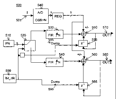
In Figure 6 is shown an alternate emdodiment of the present
invention. What is different here is the way the registers are
triggered. The bit clock, bit-clk 690, sends a dump signal 595
to the registers 655, 665, which sets the contents of the
registers 655, 665, to zero. This dump signal 695 is sent at
either the positive or negative edge of the bit clk 690. In
Figure 6 the dump signal 695 is routed differently than in
Figure 5. In Figure 6 the dump signal 695 is sent to the lower
register 665. Before reaching that register 665 it is branched
and also sent to the upper register 655.
2.0 The embodiments described above serve merely as illustration
and not as limitation. It will be apparent to one of ordinary
skill in the art that departures may be made from the
embodiments described above without departing form the spirit
and scope of the invention. The invention should not be
2.5 regarded as being limited to the examples described, but
should be regarded instead as being equal in scope to the
following claims.
SUBSTITUTE SHEET ( rule 26 )