Note: Descriptions are shown in the official language in which they were submitted.
= ~ CA 02335221 2009-06-26
~=
Doc. No. 10-329 CA. Patent
Optical Configuration for a Dynamic Gain Equalizer
and a Configurable Add/Drop Multiplexer
Field of the Invention
The present invention relates to an optical device for rerouting and modifying
an optical signal,
or more specifically, to an optical configuration including a diffraction
grating that can be used
for a dynamic gain equalizer and/or a configurable add/drop multiplexer.
Background of the Invention
In optical wavelength division multiplexed (WDM) communication systems, an
optical
waveguide simultaneously carries many different communication channels in
light of different
wavelengths. In WDM systems it is desirable to ensure that all channels have
nearly equivalent
power. To help achieve this, gain equalizers are disposed at various points
throughout the system
to control the relative power levels in respective channels.
Dense WDM systems require special add/drop multiplexers (ADM) to add and drop
particular
channels (i.e., wavelengths). For example, at predetermined nodes in the
system, optical signals
of predetermined wavelength are dropped from the optical waveguide and others
are added.
Typically, gain equalizing and add/drop multiplexer devices involve some form
of multiplexing
and demultiplexing to modify each individual channel of the telecommunication
signal. In
particular, it is common to provide a first diffraction grating for
demultiplexing the optical signal
and a second spatially separated diffraction grating for multiplexing the
optical signal after it has
been modified. An example of the latter is disclosed in U.S. Pat. No.
5,414,540. However, in
such instances it is necessary to provide and accurately align two matching
diffraction gratings
and at least two matching lenses. This is a significant limitation of prior
art devices.
1
CA 02335221 2001-02-08
Doc. No. 10-329 CA. Patent
To overcome this limitation, other prior art devices have opted to provide a
single diffraction
grating that is used to demultiplex an optical single in a first pass through.
the optics and
multiplex the optical signal in a second pass through the optics. For example,
U.S. Pat. Nos.
5,233,405, 5,526,155, 5,745,271, 5,936,752 and 5,960,133, which are
incorporated herein by
reference, disclose such devices.
However, none of these prior art devices disclose an optical arrangement
suitable for both
dynamic gain equalizer (DGE) and configurable optical add/drop multiplexer
(COADM)
applications. In particular, none of these prior art devices recognize the
advantages of providing
a simple, symmetrical optical arrangement suitable for use with various
switching/attenuating
means.
Moreover, none of the prior art devices disclose a multiplexing/demultiplexing
optical
arrangement that is compact and compatible with a plurality of parallel
input/output optical
waveguides.
For example, U.S. Pat. No. 5,414,540 to Patel et al. discloses a liquid
crystal optical switch for
switching an input optical signal to selected output channels. The switch
includes a diffraction
grating, a liquid crystal modulator, and a polarization dispersive element. In
one embodiment,
Patel et al. suggest extending the 1x2 switch to a 2x2 drop-add circuit and
using a reflector.
However, the disclosed device is limited in that the add/drop beams of light
are angularly
displaced relative to the input/output beams of light. This angular
displacement is
disadvantageous with respect to coupling the add/drop and/or input/output
beams of light into
parallel optical waveguides, in addition to the additional angular alignment
required for the input
beam of light.
With respect to compactness, prior art devices have been limited to an
excessively long and
linear configurations, wherein the input beam of light passes through each
optical component
sequentially before being reflected in a substantially backwards direction.
U.S. Pat. No. 6,081,331 discloses an optical device that uses a concave mirror
for multiple
reflections as an alternative to using two lenses or a double pass through one
lens. However, the
2
CA 02335221 2001-02-08
Doc. No. 10-329 CA. Patent
device disclosed therein only accommodates a single pass through the
diffraction grating and
does not realize the advantages of the instant invention.
It is an object of this invention to provide an optical system including a
diffraction grating that is
relatively compact.
It is a further object of the instant invention to provide an optical
configuration for rerouting and
modifying an optical signal that can be used as a dynamic gain equalizer
and/or configurable
add/drop multiplexer.
Summary of the Invention
The instant invention provides a 4-f optical system comprising a dispersive
element for spatially
separating an input optical signal into different spectral channels and a
modifying ai-ray for
selectively modifying each of the different spectral channels. At least one
element having
optical power, such as a lens or a spherical mirror, provides optical
communication between the
dispersive element and the modifying array.
Conveniently and advantageously, the dispersive element and the modifying
array are disposed
substantially at a focal plane of the at least one element having optical
power. Moreover, the
dispersive element and element having optical power are used in a first and a
second pass
through the optics, thus obviating the requirement of providing matching
elements.
In accordance with the instant invention there is provided an optical device
comprising: a first
port for launching a beam of light; first redirecting means disposed
substantially one focal length
away from the first port for receiving the beam of light, the first
redirecting means having optical
power; a dispersive element disposed substantially one focal length away from
the first
redirecting means for dispersing the beam of light into a plurality of sub-
beams of light; second
redirecting means disposed substantially one focal length away from the
dispersive element for
receiving the dispersed beam of light, the second redirecting means having
optical power; and,
modifying means optically disposed substantially one focal length away from
the second
3
CA 02335221 2001-02-08
Doc. No. 10-329 CA. Patent
redirecting means for selectively modifying each sub-beam of light and for
reflecting each of the
modified sub-beams back to the second redirecting means, wherein each sub-beam
of light is
incident on and reflected from the modifying means along substantially
parallel optical paths.
In accordance with the instant invention there is provided an optical device
for rerouting and
modifying an optical signal comprising: a first port for launching a beam of
light; a concave
reflector having a focal plane for receiving a beam of light launched from the
first port; a
dispersive element disposed substantially at the focal plane for spatially
dispersing a beam of
light reflected by the concave reflector and for redirecting a spatially
dispersed beam of light
back to the concave reflector; and modifying means disposed substantially at
the focal plane for
modifying the spatially dispersed beam of light reflected by the concave
reflector and for
reflecting the modified spatially dispersed beam of light back to one of the
first port and a second
port via the concave reflector and the dispersive element.
In accordance with the instant invention there is further provided a method of
rerouting and
modifying an optical signal comprising the steps of: launching a beam of light
towards an
element having optical power off an optical axis thereof; redirecting the beam
of light incident
on the element having optical power to a dispersive element disposed
substantially one focal
length away from the element having optical power; spatially dispersing the
redirected beam of
light into a plurality of different sub-beams of light corresponding to a
plurality of different
spectral channels with a dispersive element disposed substantially one focal
length away from
the element having optical power; redirecting the plurality of different sub-
beams of light to a
modifying means optically disposed substantially two focal lengths away from
the dispersive
element; selectively modifying the plurality of different sub-beams of light
and reflecting them
in a substantially backwards direction; and redirecting the selectively
modified plurality of
different sub-beams to the dispersive element and combining them to fornl a
single output beam
of light, wherein the plurality of different sub-beams of light and the
selectively modified
plurality of different sub-beams follow substantially parallel optical paths
to and from the
modifying means, respectively.
4
- ------------
! CA 02335221 2001-02-08
Doc. No. 10-329 CA. Patent
In accordance with the instant invention there is provided an optical device
for rerouting and
modifying an optical signal comprising: a lens including a first end having a
single port
coincident with an optical axis thereof and a second end having two ports
disposed off the optical
axis; an element having optical power disposed about one focal length away
from the lens for
receiving a beam of light launched from the single port; a dispersive element
disposed about one
focal length away from the element having optical power for spatially
dispersing a beam of light
received therefrom; and modifying means optically disposed about two focal
lengths away from
the dispersive element for modifying and reflecting a beam of light spatially
dispersed by the
dispersive element, wherein said one focal length is a focal length of the
element having optical
power.
In accordance with the instant invention there is provided a method of
modifying and rerouting a
beam of light comprising the steps of: launching the beam of light through a
first port disposed
about a first end of a lens off the optical axis of the lens, the beam of
light launched in a direction
parallel to the optical axis; allowing the beam of light to pass through the
lens to a single port
disposed about an opposite side of the lens coincident with the optical axis,
and allowing the
beam of light to exit the single port at a first predetermined angle to the
optical axis; modifying
the beam of light and reflecting the modified beam of light back to the single
port at a second
predetermined angle to the optical axis; and, allowing the modified beam of
light to pass through
the lens to a second port disposed about the first end of the lens, the second
port disposed off the
optical axis and spatially separated from the first port.
Brief Description of the Drawings
Exemplary embodiments of the invention will now be described in conjunction
with the
drawings in which:
Fig. I is a schematic diagram illustrating an embodiment of an optical
configuration that can be
used as a dynamic gain equalizer and/or add-drop multiplexer (DGE/COADM) in
accordance
with the invention;
5
CA 02335221 2001-02-08
Doc. No. 10-329 CA. Patent
Fig. 2a is a detailed side view of a front-end module for use with the
DGE/COADM shown in
Fig. 1 having means for compensating for polarization mode dispersion (PMD);
Fig. 2b is a detailed side view of an alternative front-end module having
means for reducing or
substantially eliminating PMD;
Fig. 3a is a top view of one embodiment of modifying means comprising a liquid
crystal array
for use with the DGE/COADM shown in Fig. 1, wherein a liquid crystal element
is switched to
1o an ON state;
Fig. 3b is a top view of the modifying means shown in Fig. 3a, wherein the
liquid crystal element
is switched to an OFF state;
Fig. 3c is a top view of another embodiment of the modifying means for use
with the
DGE/COADM shown in Fig. 1, wherein the liquid crystal element is switched to
an ON state;
Fig. 3d is a top view of the modifying means shown in Fig. 3c, wherein the
liquid crystal element
is switched to an OFF state;
Fig. 4a is a top view of another embodiment of the modifying means for use
with the
DGE/COADM shown in Fig. 1 having a birefringent crystal positioned before the
liquid crystal
array, wherein the liquid crystal element is switched to an OFF state;
Fig. 4b is a top view of the modifying means shown in Fig. 4a, wherein the
liquid crystal element
is switched to an ON state;
Fig. 5 is a top view of yet another embodiment of the modifying means for use
with the DGE
shown in Fig. 1 utilizing a MEMS device;
6
CA 02335221 2001-02-08
Doc. No. 10-329 CA. Patent
Figs. 6a and 6b are schematic diagrams of an embodiment of the invention that
is preferred over
the one shown in Fig. 1, wherein the focal plane of a single concave reflector
is used to locate the
input/output ports, diffraction grating, and modifying means;
Fig. 7 is a schematic diagram of an embodiment of the invention that is
similar to that shown in
Figs. 6a and 6b, wherein the input/output ports are disposed between the
modifying means and
dispersive element;
Fig. 8 is a schematic diagram of a DGE having a configuration similar to that
shown in Figs. 6a
1o and 6b including an optical circulator; and
Fig. 9 is a schematic diagram of a DGE/COADM in accordance with the instant
invention
including a lens having a single port for launching and receiving light from
the concave reflector;
Fig. 9a is a top view showing a lenslet array coupling input/output optical
waveguides to the lens
in accordance with the instant invention;
Fig. 9b is a top view showing a prior art polarization diversity arrangement
coupling input/output
optical waveguides to the lens in accordance with the instant invention;
Fig. 9c is a side view of the prior art polarization diversity arrangement
shown in Fig. 9b;
Fig. 9d is a top view showing an alternative arrangement to the optical
components shown in Fig.
9b;
Fig. 9e is a side view of the alternate arrangement shown in Fig. 9d;
Fig. 9f is a top view showing an asymmetric offset of the input/output optical
waveguides with
respect to the optical axis of the lens, in accordance with the instant
invention;
7
CA 02335221 2001-02-08
Doc. No. 10-329 CA. Patent
Fig. 10 is a schematic diagram of another embodiment of a DGE/COADM in
accordance with
the invention;
Fig. 11 is a schematic diagram of the preferred embodiment of a COADM in
accordance with the
instant invention; and,
Fig. 12 is a schematic diagram of a COADM in accordance with the instant
invention, wherein
an asymmetric arrangement of the input/output optical waveguides complements
the angular
displacement provided by a MEMS element.
Detailed Description
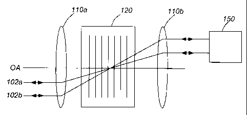
Referring now to Fig. 1, an optical device for rerouting and modifying an
optical signal in
accordance with the instant invention is shown that is capable of operating as
a Dynamic
Gain/Channel Equalizer (DGE) and/or a Configurable Optical Add/Drop
Multiplexer (COADM).
The optical design includes a diffraction element 120 disposed between and at
a focal plane of
identical elements 110a and 110b having optical power, respectively. Two ports
102a and 102b
are shown at an input/output end with bi-directional arrows indicating that
light launched into
port 102a can be transmitted through the optical device and can be reflected
backward to the
input port from which it was launched 102a, or alternatively, can be switched
to port 102b or
vice versa in a controlled manner. The input/output ports 102a and 102b are
also disposed about
one focal plane away from the element having optical power 110a to which they
are optically
coupled. Although only two input/output ports are shown to facilitate an
understanding of this
device, a plurality of such pairs of ports is optionally provided. At the
other end of the device,
modifying means 150 for modifying at least a portion of the light incident
thereon is provided
about the focal plane of the element having optical power 110b.
Since the modifying means and/or dispersive element are generally dependent
upon polarization
of the incident light beam, light having a known polarization state is
provided to obtain the
selected switching and/or attenuation. Figs. 2a and 2b illustrate two
different embodiments of
8
CA 02335221 2001-02-08
Doc. No. 10-329 CA. Patent
polarization diversity arrangements for providing light having a known
polarization state, for use
with the DGE/COADM devices described herein. The polarization diversity
arrangement, which
is optionally an array, is optically coupled to the input and output ports.
Referring to Fig. 2a an embodiment of a front-end micro-optical component 105
for providing
light having a known polarization is shown having a fibre tube 107, a
microlens 112, and a
birefringent element 114 for separating an input beam into two orthogonal
polarized sub-beams.
At an output end, a half waveplate 116 is provided to rotate the polarization
of one of the beams
by 90 so as to ensure both beams have a same polarization state e.g.,
horizontal. A glass plate or
a second waveplate 118 is added to the fast axis path of the crystal 114 to
lessen the effects of
Polarization Mode Dispersion (PMD) induced by the difference in optical path
length along the
two diverging paths of crystal 114.
Fig. 2b illustrates an alternative embodiment to that of Fig. 2a, wherein two
birefringent
elements 114a, 114b have a half waveplate 1 16a disposed therebetween; here an
alternate
scheme is used to make the path lengths through the birefringent materials
substantially similar.
Optionally, a third waveplate 119 is provided for further rotating the
polarization state.
Although, Figs. 2a and 2b both illustrate a single input beam of light for
ease of understanding,
the front end unit 105 is capable of carrying many more beams of light
therethrough, in
accordance with the instant invention (i.e., can be designed as an array as
described above).
Figs. 3a-3b, 3c-3d, 4, and 5, each illustrate a different embodiment of the
modifying means for
use with the DGE/COADM devices described herein. Each of these embodiments is
described
in more detail below. Note that the modifying means are generally discussed
with reference to
Fig. 1. However, although reference is made to the dispersive element 120 and
elements having
optical power 110a and 110b, these optical components have been omitteci from
Figs. 3a-3b, 3c-
3d, 4, and 5 for clarity.
9
CA 02335221 2001-02-08
Doc. No. 10-329 CA. Patent
Referring to Figs. 3a and 3b a schematic diagram of the modifying means 150 is
shown
including a liquid crystal array 130 and a reflector 140. The reflector
includes first and second
polarizing beam splitters 144 and 146, and reflective surface 142.
When the device operates as a COADM, each pixel of the liquid crystal array
130 is switchable
between a first state e.g., an "ON" state shown in Fig. 3a, wherein the
polarization of a beam of
light passing therethrough is unchanged (e.g., remains horizontal), and a
second state e.g., an
"OFF" state shown in Fig. 3b, wherein the liquid crystal cell rotates the
polarization of a beam of
light passing therethrough 90 (e.g., is switched to vertical). The reflector
140 is designed to pass
light having a first polarization (e.g., horizontal) such that beam of light
launched from port 102a
is reflected back to the same port, and reflect light having another
polarization (e.g., vertical)
such that a beam of light launched from port 102a is switched to port 102b.
When the device operates as a DGE, each liquid crystal cell is adjusted to
provide phase
retardations between 0 to 180 . For a beam of light launched and received from
port 102a, 0%
attenuation is achieved when liquid crystal cell provides no phase retardation
and 100%
attenuation is achieved when the liquid crystal cell provides 180 phase
retardation. Intermediate
attenuation is achieved when the liquid crystal cells provide a phase
retardation greater than 0
and less than 180 . In some DGE applications, the reflector 140 includes only
a reflective
surface 142 (i.e., no beam splitter).
Preferably, the liquid crystal array 130 has at least one row of liquid
crystal cells or pixels. For
example, arrays comprising 64 or 128 independently controlled pixels have been
found
particularly practical, but more or fewer pixels are also possible.
Preferably, the liquid crystal
cells are of the twisted nematic type cells, since they typically have a very
small residual
birefringence in the "ON" state, and consequently allow a very high contrast
ratio (>35 dB) to be
obtained and maintained over the wavelength and temperature range of interest.
It is also
preferred that the inter-pixel areas of the liquid crystal array 130 are
covered by a black grid.
Figs. 3c and 3d are schematic diagrams analogous to Figs. 3a and 3b
illustrating an alternate
form of the modifying means 150 discussed above, wherein the reflector 140
includes a double
CA 02335221 2001-02-08
Doc. No. 10-329 CA. Patent
Glan prism. The arrangement shown in Figs. 3c and 3d is preferred over that
illustrated in Figs.
3a and 3b, since the respective position of the two-sub beams emerging from
the polarization
diversity arrangement (not shown) does not change upon switching.
Note that in Figs. 3a-3d, the dispersion direction is perpendicular to the
plane of the paper. For
exemplary purposes a single ray of light is shown passing through the
modifying means 150.
Figs. 4a and 4b are schematic diagrams showing another embodiment of the
modifying means
150, wherein a birefringent crystal 152 is disposed before the liquid crystal
array 130. A beam of
light having a predetermined polarization state launched from port 102a is
dispersed into sub-
beams, which are passed through the birefringent crystal 152. The sub-beams of
light passing
through the birefringent crystal 152 remain unchanged with respect to
polarization. The sub-
beams of light are transmitted through the liquid crystal array 130, where
they are selectively
modified, and reflected back to the birefringent crystal 152 via reflective
surface 142. If a
particular sub-beam of light passes through a liquid crystal cell in an "OFF"
state, as shown in
Fig. 4a, then the polarization thereof will be rotated by 90 and the sub-beam
of light will be
refracted as it propagates through the birefringent crystal 152 before being
transmitted to port
102b. If the sub-beam of light passes through a liquid crystal cell in an "ON"
state, as shown in
Fig. 4b, then the polarization thereof will not be rotated and the sub-beam of
light will be
transmitted directly back to port 102a. A half wave plate 153 is provided to
rotate the
polarization of the refracted sub-beams of light by 90 to ensure that both
reflected beams of
light have a same polarization state.
Fig. 5 is a schematic diagram of another embodiment of the modifying means 150
including a
micro electro-mechanical switch (MEMS) 155, which is particularly useful when
the device is
used as a DGE. A beam of light having a predetermined polarization state
launched from port
102a is dispersed into sub-beams and is passed through a birefringent element
156 and quarter
waveplate 157. The birefringent element 156 is arranged not to affect the
polarization of the
sub-beam of light. After passing through the quarter waveplate 157, the beam
of light becomes
circularly polarized and is incident on a predetermined reflector of the MF:MS
array 155. The
reflector reflects the sub-beam of light incident thereon back to the quarter
waveplate. The
11
CA 02335221 2001-02-08
Doc. No. 10-329 CA. Patent
degree of attenuation is based on the degree of deflection provided by the
reflector (i.e., the angle
of reflection). After passing through the quarter waveplate 157 for a second
time, the attenuated
sub-beam of light will have a polarization state that has been rotated 90
from the original
polarization state. As a result the attenuated sub-beam is refracted in the
birefringent element
156 and is directed out of the device to port 102b. A half wave plate 158 is
provided to rotate the
polarization of the refracted sub-beams of light by 90 .
Of course, other modifying means 150 including at least one optical element
capable of
modifying a property of at least a portion of a beam of light and reflecting
the modified beam of
1o light back in substantially the same direction from which it originated are
possible.
Advantageously, each of the modifying means discussed above utilizes an
arrangement wherein
each spatially dispersed beam of light is incident thereon and reflected
therefrom at a 90 angle.
The 90 angle is measured with respect to a plane encompassing the array of
modifying elements
(e.g., liquid crystal cells, MEMS reflectors). Accordingly, each sub-beam of
light follows a first
optical path to the modifying means where it is selectively switched such that
it is reflected back
along the same optical path, or alternatively, along a second optical path
parallel to the first. The
lateral displacement of the input and modified output beams of light (i.e., as
opposed to angular
displacement) allows for highly efficient coupling between a plurality of
input/output
waveguides. For example, the instant invention is particular useful when the
input and output
ports are located on a same multiple bore tube, ribbon, or block.
In order to maintain the desired simplicity and symmetry, it is preferred that
the element having
optical power be rotationally symmetric, for example a rotationally symmetric
lens or spherical
reflector. Preferably, the spherical reflector is a concave mirror. Moreover,
it is preferred that
the diffraction element 120 be a high efficiency, high dispersion diffraction
grating. Optionally,
a circulator (not shown) is optically coupled to each of ports 102a and 102b
for separating
input/output and/or add/drop signals.
Referring again to Fig. 1, the operation of the optical device operating as a
COADM is described
by way of the following example. A collimated beam of light having a
predetermined
12
CA 02335221 2001-02-08
Doc. No. 10-329 CA. Patent
polarization and carrying wavelengths Xt, X2, ... X8 is launched through port
102a to a lower
region of lens 110a and is redirected to the diffraction grating 120. The beam
of light is spatially
dispersed (i.e., demultiplexed) according to wavelength in a direction
perpendicular to the plane
of the paper. The spatially dispersed beam of light is transmitted as 8 sub-
beams of light
corresponding to 8 different spectral channels having central wavelengths Xt,
~12, ... Xs through
lens 110b, where it is collimated and incident on the modifying means 150,
which for exemplary
purposes, is shown in Fig. 3a-b. Each sub-beam of light is passed through an
independently
controlled pixel in the liquid crystal array 130. In particular, the sub-bearn
of light having central
wavelength X3 passes through a liquid crystal cell in an "OFF" state, and each
of the other 7
channels having central wavelengths Xt-X2 and 4X8 pass through liquid crystal
cells in an "ON"
state. As the sub-beam of light having central wavelength X3 passes through
the liquid crystal in
the "OFF" state, the polarization thereof is rotated 90 , it is reflected by
the polarization beam
splitter 144 towards a second beam splitter 146, and is reflected back to port
102b, as shown in
Fig. 3b. As the other 7 channels having central wavelengths XI-X2 and X4-X8
pass through liquid
crystal cells is in an "ON" state, the polarizations thereof remain unchanged,
and they are
transmitted through the polarization beam splitter 144 and are reflected off
reflective surface 142
back to port 102a. In summary, the beam of light originally launched frorn
port 102a will return
thereto having dropped a channel (i.e., having central wavelength X3) and the
sub-beam of light
corresponding to the channel having central wavelength X3 will be switched to
port 102b.
Simultaneously, a second beam of light having a predetermined polarization and
carrying
another optical signal having a central wavelength X3 is launched from port
102b to a lower
region of lens 110a. It is reflected from the diffraction grating 120, and is
transmitted through
lens 1 lOb, where it is collimated and incident on the modifying means 150.
The second beam of
light passes through the liquid crystal cell in the "OFF" state, the
polarization thereof is rotated
90 , it is reflected by the second polarization beam splitter 146 towards the
first beam splitter
144, and is reflected back to port 102a, as shown in Fig. 3b. Notably, the 7
express channels and
the added channel are multiplexed when they return via the dispersion grating
120.
Since every spectral channel is passed through an independently controlled
pixel before being
13
CA 02335221 2001-02-08
Doc. No. 10-329 CA. Patent
reflected back along one of the two possible optical paths, a full
reconfigurablility of plurality of
channels is obtained.
Notably, the choice of eight channels is arbitrarily chosen for exemplary
purposes. More or
fewer channels are also within the scope of the instant invention.
Referring again to Fig.1, the operation of the optical device operating as a
DGE is described by
way of the following example. A collimated beam of light having a
predetermined polarization
and carrying channels ;~I, X2, ... X8 is launched from port 102a through lens
110a, where it is
redirected to diffraction grating 120. The beam of light is spatially
dispersed according to
wavelength in a direction perpendicular to the plane of the paper. The
spatially dispersed beam
of light is transmitted as 8 sub-beams of light corresponding to 8 different
spectral channels
having central wavelengths X1, X2, ... X8 through lens 110b, where it is
collimated and incident
on the modifying means 150 such that each sub-beam of light is passed through
an independently
controlled pixel in the liquid crystal array 130 wherein the polarization of
each sub-beam of light
is selectively adjusted. In particular, the sub-beam of light having central
wavelength X3 is
passed through a liquid crystal cell in an "ON" state, the polarization
thereof is not adjusted, it
passes through the beam splitter 144, and is reflected back to port 102a with
no attenuation, as
illustrated in Fig. 3a. Simultaneously, a sub-beam of light having central
wavelength x4 is
passed through a liquid crystal cell in an "OFF" state, the polarization
thereof is rotated by 90 , it
is reflected from beam splitters 144 and 146 and is directed to port 102b.
100% attenuation is
achieved with respect to this sub-beam of light returning to port 102a.
Simultaneously, a sub-
beam of light having central wavelength X5 is passed through a liquid crystal
cell that provides
phase retardation between 0 and 180 , it is partially transmitted through from
beam splitter 144
and returns to port 102a an attenuated signal. The degree of attenuation is
dependent upon the
phase retardation.
Optionally, a second beam of light is simultaneously launched from port 102b
into the optical
device for appropriate attenuation. In fact, this optical arrangement provides
a single optical
system that is capable of providing simultaneous attenuation for a plurality
of input ports, e.g.,
102c, 102d, 102e, etc ....(not shown).
14
CA 02335221 2001-02-08
Doc. No. 10-329 CA. Patent
Alternatively, the attenuated light is received from port 102b, hence
obviating the need for a
circulator. In this instance, when the polarization of a beam of light having
central wavelength X3
is rotated by 90 (i.e., the liquid crystal array provides 180 phase
retardation), it is reflected
from the beam splitter 144 to the second beam splitter 146 (shown in Fig. 3a)
and is directed to
port 102b with no attenuation. Similarly, when the polarization of this beam
of light is not
adjusted (i.e., the liquid crystal array provides no phase retardation), it
passes through the beam
splitter 144 (shown in Fig. 3a) and is reflected back to port 102a. 100%
attenuation with respect
to this sub-beam of light reaching port 102b is achieved. Variable attenuation
is achieved when
lo the liquid crystal cell selectively provides phase retardation between 0
and 180 .
Turning now to Fig. 6a another embodiment of the DGE/COADM which is preferred
over the
embodiment shown in Fig. 1, is shown. For clarity, only one beam is shown
exiting the front-end
unit 605, however at least one other beam (not shown) is disposed behind this
beam as is evident
in the isometric view illustrated in Fig. 6b.
In Fig. 6a a single element having optical power in the form of a spherical
reflector 610 is used
to receive a collimated beam of light from the front-end unit 605 and to
receive and reflect
beams of light to and from the diffraction grating 620 and the modifying
rneans 650. The front-
end unit 605, the diffraction grating 620, and the modifying means 650, are
similar to parts 105,
120, and 150 described above. However, in this embodiment the front-end unit
605, the
diffraction grating 620, and the modifying means are each disposed about the
single focal plane
of the spherical reflector 610. Preferably, the diffraction grating is further
disposed about the
optical axis of the spherical reflector 610. In general, two circulators (not
shown) are optically
coupled to the front-end unit 605 to separate input/out and add/drop signals
in ports 102a and
102b, as described above.
Preferably, the diffraction grating 620, the spherical reflector 640, and the
modifying means 650
are each made of fused silica and mounted together with a beam folding mirror
or prism 660 to a
supporting plate 670 made of the same, as illustrated in Fig. 6b. The beain
folding mirror or
prism 660 is provided for space considerations. Advantageously, this design
provides stability
CA 02335221 2001-02-08
Doc. No. 10-329 CA. Patent
with respect to small temperature fluctuations. Moreover, this design is
clefocus free since the
radius of curvature of the spherical reflector 610 changes in proportion to
thermal expansion or
contraction of any other linear dimensions. Advantageously, the spherical
mirror 610 has
substantially no chromatic aberrations.
When the optical device operates as a DGE, a detector array 657 is optionally
positioned behind
the beam-folding mirror 660 to intercept part of the wavelength dispersed beam
of light. This
design allows the signal to be tapped while eliminating the need for external
feedback.
Preferably, the diffraction grating 620 and the modifying means 650 are
disposed substantially
one focal length away from the spherical mirror 610 or substantially at the
focal plane of the
spherical reflector 610, as discussed above. For example, in COADM
applications it is prefetred
that the modifying means 650 are substantially at the focal plane to within
10% of the focal
length. For DGE applications, it is preferred that the modifying means 650 are
substantially at
the focal plane to within 10% of the focal length if a higher spectral
resolution is required,
however, the same accuracy is not necessary for lower resolution applications.
In operation, a multiplexed beam of light is launched into the front-end urtit
605. The
polarization diversity arrangement 105 provides two substantially collimated
sub-beams of light
having the same polarization (e.g., horizontal), as discussed above. The two
beams of light are
transmitted to the spherical reflector 610 and are reflected therefrom towards
the diffraction
grating 620. The diffraction grating 620 separates each of the two sub-beams
into a plurality of
sub-beams of light having different central wavelengths. The plurality of sub-
beams of light are
transmitted to the spherical reflector 610 where they are collimated and
transmitted to the
modifying means 150 where they are incident thereon as spatially separated
spots corresponding
to individual spectral channels. Each sub-beam of light corresponding to an
individual spectral
channel is modified and reflected backwards either along the same optical path
or another optical
path according to its polarization state, as described above. The sub-beams of
light are
transmitted back to the spherical reflector 610 and are redirected to the
dispersive element, where
they are recombined and transmitted back to the spherical element to be
transmitted to the
predetermined input/output port.
16
CA 02335221 2001-02-08
Doc. No. 10-329 CA. Patent
Optionally, second, third, forth, ... etc. multiplexed beams of light are
launched into the front-
end unit 605. In fact, this optical arrangement is particularly useful for
applications requiring
the manipulation of two bands (e.g., C and L bands), simultaneously, wherein
each band has its
own corresponding in/out/add/drop ports.
Advantageously, the optical arrangement shown in Figs. 6a and 6b provides a
symmetrical 4-f
optical system with fewer alignment problems and less loss than prior art
systems. In fact, many
of the advantages of this design versus a conventional 4f system using
separate lenses is afforded
1o due to the fact that the critical matching of components is obviated. One
significant advantage
relates to the fact that the angle of incidence on the grating, in the first
and second pass, is
inherently matched with the optical arrangement.
The instant invention further provides an optical device for rerouting and
modifying an optical
signal device that is substantially more compact and that uses substantially
fewer components
than similar prior art devices.
Fig. 7 shows an alternate arrangement of Fig. 6a and Fig. 6b that is
particularly compact. In this
embodiment, the more bulky dispersive element 620 and modifying means 650 are
disposed
outwardly from the narrower front-end unit 605.
Fig. 8 illustrates a DGE including a conventional three port optical
circulator and having a
particularly symmetrical design. A beam of light is launched into a first port
882 of the circulator
880 where it circulates to and exits through port 884. The beam of light
exiting port 884 is
passed through the front-end unit 805, which produces two collimated sub-beams
having a same
polarization that are transmitted to an upper region of the spherical
reflector 810 in a direction
parallel to an optical axis OA thereof. The collimated sub-beams of light
incident on the
spherical reflector 810 are reflected and redirected to the diffraction
grating 820 with an angle of
incidence P. The sub-beams of light are spatially dispersed according to
wavelength and are
transmitted to a lower region of the spherical reflector 810. The spatially
dispersed sub-beams of
light incident on the lower region of the spherical reflector 810 are
reflected and transmitted to
17
CA 02335221 2001-02-08
Doc. No. 10-329 CA. Patent
the modifying means 850 in a direction parallel to the optical axis of the
spherical reflector 810.
Once attenuated, the sub-beams of light are reflected back to the spherical
reflector 810, the
diffraction grating 820, and the front-end unit 805 along the same optical
path. The diffraction
grating recombines the two spatially dispersed sub-beams of light. The front-
end unit 805
recombines the two sub-beams of light into a single beam of light, which is
transmitted to the
circulator 880 where it is circulated to output port 886. The front-end unit
805, diffraction
grating 820, and modifying means 850, which are similar to components 105,
120, and 150
described above, are each disposed about a focal plane 825 of the spherical
reflector 810. In
particular, the diffraction grating 820 is disposed about the focal point of
the spherical reflector
810 and the modifying means 850 and front-end unit are symmetrically disposed
about the
diffraction grating. Preferably, the modifying means 850 includes either a
liquid crystal array
830 and a flat reflector 840, or a MEMS array (not shown).
Notably, an important aspect of the optical design described heretofore
relates to the symmetry
and placement of the optical components. In particular, the fact that each of
the front-end unit,
the element having optical power, the dispersive element, and the modifying
means are disposed
about one focal length (of the element having optical power) away from each
other is particularly
advantageous with respect to the approximately Gaussian nature of the incident
beam of light.
Referring again to Fig. 8, the input beam of light emerges from the front-end
unit 805 essentially
collimated and is transmitted via the element having optical power 810 to the
diffraction grating
820. Since the diffraction grating 820 is located at the focus of the element
having optical power
810 and the input beams are collimated, the light is essentially focused on
the diffraction gt-ating
820, as discussed above. The 1/e2 spot size at the grating, 2wi, and the 1/e2
diameter 2cn2 at the
front-end unit 805, are related by:
w, *"=;~*f/n
where X is wavelength and f is the focal length of the element having optical
power.
Accordingly, one skilled in the art can tune the spot size on the diffraction
grating 820 and the
resulting spectral resolution by changing the beam size at the front-end unit
805.
18
CA 02335221 2001-02-08
Doc. No. 10-329 CA. Patent
Moreover, the instant invention allows light beams launched from the front-end
unit 805 to
propagate to the liquid crystal array 830 with little or no spot expansion,
since by symmetry, the
spot size at the liquid crystal array is the same as the spot size at the
front-end unit. Accordingly,
the size of a beam of light launched from the front-end unit 805 can be
changed to conform to
the cell size of the liquid crystal array and/or vice versa. Alternatively,
the size of the beam of
light can be adjusted to change the spot size on the grating element 820, as
discussed above.
Obviously, the same tuning is achievable with the optical arrangements shown
in both Fig. 1 and
Figs. 6a, 6b.
Fig. 9 illustrates an embodiment in accordance with the instant invention,
wherein a single
collimating/focusing lens 990 replaces the optical circulator 884 in the DGE
shown in Fig. 8.
Preferably, the lens 990 is a collimating/focusing lens such as a Graded Index
or GRIN lens.
The GRIN lens 990 is disposed such that an end face 994 thereof is coincident
with the focal
plane 925 of the spherical reflector 910. The GRIN lens 990 is orientated such
that its optical
axis (OA2) is parallel to but not coaxial with the optical axis OA of the
spherical reflector 990.
Input 985 and output 987 ports are disposed about an opposite end face 993 of
the lens 990, off
the optical axis OAz, and are optically coupled to input 999 and output 998
optical waveguides,
respectively. Preferably, input 999 and output 998 waveguides are optical
fibres supported by a
double fibre tube, such as a double bore tube or a double v-groove tube. A
single input/output
port 992 is disposed about end face 994 coincident with the optical axis OA2.
The modifying
means 950 are shown including a liquid crystal array 930 and a flat mirror 940
perpendicular to
the OA of the spherical reflector 910. Alternatively, the modifying means
comprises a MEMS
array (not shown). All other optical components are similar to those described
with reference to
Fig. 8.
In operation, a beam of light is launched from input waveguide 999 into port
985 in a direction
substantially parallel to the optical axis (OAZ) of the lens 990. The beam of
light passes through
the GRIN lens 990, and emerges from port 992 at an angle a to the optical
axis. The angle a is
dependent upon the displacement of port 985 from the optical axis (OA2), d.
The beam of light
is transmitted to an upper end of the spherical reflector 910, where it is
directed to the diffraction
19
CA 02335221 2001-02-08
Doc. No. 10-329 CA. Patent
grating 920 with an angle of incidence P. The resulting spatially dispersed
beam of light is
transmitted to the spherical reflector, is reflected, and is transmitted to
the modifying means 950.
If the diffraction grating 920 is parallel to the focal plane 925, as shown in
Fig. 9, the beam of
light incident on the modifying means has an angle of incidence substantially
close to a. Each
sub-beam of the spatially dispersed beam of light is selectively reflected
back to the spherical
reflector 910 at a predetermined angle, generally along a different optical
path from which it
came. Variable attenuation is provided by the modifying means 950. The
spherical reflector 910
redirects the modified spatially dispersed beam of light back to the
diffraction grating 920 such
that it is recombined to form a single modified output beam of light, which is
incident on the
1o single port 992 with an angle of incidence close to -a. The attenuated
output beam of light is
passed through the lens 990, and is directed towards output port 987 whei-e it
is transmitted to
output optical fibre 998.
Advantageously, this simple device, which allows light to enter and exit
through two different
ports disposed at one end of the device, is simple, compact, and easy to
manufacture relative to
prior art modifying and rerouting devices.
Moreover, the instant design obviates the need for a bulky and costly optical
circulator, while
simultaneously providing an additional degree of freedom to adjust the mode
size, which in part
defines the resolution of the device (i.e., can adjust the focal length of
GRIN lens 990).
Preferably, light transmitted to and from the output 998 and input 999 optical
waveguides is
focussed/collimated, e.g., through the use of microcollimators, thermally
expanded core fibres,
or lens fibres. Optionally, a front-end unit (e.g., as shown in Figs. 2a or
2b), which is in the form
of an array, couples input/output waveguides 999/998 to end face 993. Figs. 9a-
9d illustrate
various optical input arrangements, which for exemplary purposes are
illustrated with the
arrangement shown in Fig. 2a.
In Fig. 9a, the input 999 and output 998 optical fibres are coupled to the
GRIN lens 990 via a
lenslet array 912. A spacer 913 is provided in accordance with the preferred
telecentric
CA 02335221 2001-02-08
Doc. No. 10-329 CA. Patent
configuration. This optical arrangement, which does not provide polarization
diversity, is
suitable for applications that do not involve polarization sensitive
components.
Figs. 9b and 9c depict top and side views of the embodiment where a front-end
unit (i.e., as
shown in Fig. 2a), couples the input/output waveguides 999/998 to the GRIN
lens 990. More
specifically, the front-end unit includes sleeve 996, lenslet array 912,
birefringent element 914,
half waveplates 916, glass plates or second waveplates 918, and GRIN letis
990.
In Figs. 9d and 9e there is shown top and side views of an arrangement wherein
the birefringent
element 914, half waveplates 916, and glass plates 918, which provide the
polarization diversity,
are disposed about end face 994 of GRIN lens 990 and a spacer 913 the lenslet
array 112 are
disposed about end face 993.
Fig. 9f illustrates an embodiment wherein the input 999 and output 998 optical
waveguides are
not symmetrically disposed about the optical axis OAz of the GRIN lens 990. In
these instances,
it is more convenient to compare the fixed distance between the input 999 and
output 998
waveguides (D=2d) to the total angle between the input and output optical
paths (2(X). More
specifically, the relationship is given approximately as:
D = 2a
F
where F is the focal length of the GRIN lens 990.
Of course other variations in the optical arrangement are possible. For
example, in some
instances, it is preferred that the diffraction grating 920 is disposed at an
angle to the focal plane
925. In addition, the placement of the front end unit/lens 990, diffraction
grating 920, and
modifying means 950 can be selected to minimize aberrations associated with
the periphery of
the element having optical power 910. In Fig. 10, an alternative design of
Fig. 9, wherein the
element having optical power is a lens 910 having two focal planes, 925a and
925b is illustrated.
The diffraction grating 920 is coincident with focal plane 925b and the
reflector 940 is
21
CA 02335221 2001-02-08
Doc. No. 10-329 CA. Patent
coincident with focal plane 925a. The operation is similar to that discussed
for Fig. 9.
An advantage of the embodiments including a GRIN lens 990, e.g. as shown in
Fig. 9-9d is that
they are compatible with modifying means based on MEMS technology, for both
COADM and
DGE applications. This is in contrast to the prior art optical arrangements
described in Figs. 1
and 6-8, wherein the MEMS based modifying means 150 are preferred for DGE
applications
over COADM applications.
In particular, when the single collimating/focusing lens 990 provides the
input beam of light and
receives the modified output beam of light, the angular displacement provided
by each MEMS
reflector complements the angular displacement resulting from the use of the
off-axis
input/output port(s) on the GRIN lens 990. More specifically, the angular
displacement provided
by the lens 990 e.g., a, is chosen in dependence upon the angular displacement
of the MEMS
device, e.g., 1 .
A preferred embodiment is illustrated in Fig. 11, wherein an arrangement
similar to that shown
in Fig. 9 designed to operate as a COADM, is shown. Optical circulators 80a
and 80b are
coupled to each of the optical waveguides 99a and 99b, respectively, for
separating in/out and
add/drop optical signals. Optical waveguides 99a and 99b are optically coupled
to microlenses
12a and 12b disposed on one side of the lens 90.
The lens 90 is disposed such that an end thereof lies in the focal plane 25 of
the spherical
reflector 10. Also in the focal plane are the dispersive element 20 and the
modifying means 50,
as described above. However, in this embodiment, the modifying means is
preferably a MEMS
array 50. Notably, the MEMS array provides a 2x2 bypass configuration wherein
an express
signal launched into port 1 of the circulator 80a propagates to port 3 of the
same circulator 80a in
a first mode of operation and a dropped signal launched into port one of the
circulator 80a
propagates to port 3 of the second circulator 80b in a second mode of
operation. Similarly, a
signal added at port 1 of the second circulator device propagates to port 3 of
the second
circulator in the second mode of operation and is not collected in the first
mode of operation.
For exemplary purposes, the beam of light is assumed to include wavelengths X,
and X2,
however, in practice more wavelengths are typically used.
22
CA 02335221 2001-02-08
Doc. No. 10-329 CA. Patent
In operation, the beam of light carrying wavelengths X1 and X2, is launched
into port 1 of the first
optical circulator 80a and is circulated to optical waveguide 99a supported by
sleeve 96. The
beam of light is transmitted through the microlens 12a to the lens 90, in a
direction substantially
parallel to the optical axis (OAz) of the lens 90. The beam of light enters
the lens through port
85 disposed off the optical axis (OA2) and emerges from port 92 coincident
with the optical axis
(OA2) at an angle to the optical axis (OA2). The emerging beam of light X1X2,
is transmitted to
an upper portion of the spherical reflector 10, is reflected, and is incident
on the diffraction
grating 20, where it is spatially dispersed into two sub-beams of light
carrying wavelengths Xi
and X2, respectively. Each sub-beam of light is transmitted to a lower portion
of the spherical
reflector 10, is reflected, and is transmitted to separate reflectors 51 and
52 of the MEMS array
50. Referring to Fig. 11, reflector 51 is orientated such that the sub-beam of
light corresponding
to Xt incident thereon, is reflected back along the same optical path to the
lens 90, passes
through port 85 again, and propagates to port 2 of circulator 80a where it is
circulated to port 3.
Reflector 52, however, is orientated such that the sub-beam of light
corresponding to X2 is
reflected back along a different optical path. Accordingly, the dropped signal
corresponding to
wavelength Xz is returned to the lens 90, passes through port 87, propagates
to port 2 of the
second circulator 80b, and is circulated to port 3.
Simultaneously, a second beam of light having central wavelength X2 is added
into port I of the
second optical circulator 80b and is circulated to optical waveguide 99b. The
second beam of
light X2 is transmitted through the microlens 12b to the lens 90, in a
direction substantially
parallel to the optical axis (OA2) of the lens 90. It enters the lens 90
through port 87 disposed off
the optical axis (OAz) and emerges from port 92 coincident with the optical
axis (OAz) at an
angle to the optical axis. The emerging beam of light is transmitted to an
upper portion of the
spherical reflector 10, is reflected, and is incident on the diffraction
grating 20, where it is
reflected to reflector 52 of the MEMS array 50. Reflector 52 is orientated
such that the second
beam of light corresponding to X2 is reflected back along a different optical
path to the spherical
reflector 10, where it is directed to the diffraction grating. At the
diffraction grating, the added
optical signal corresponding to XZ is combined with the express signal
corresponding to X I. The
23
CA 02335221 2001-02-08
Doc. No. 10-329 CA. Patent
multiplexed signal is returned to the lens 90, passes through port 85, and
returns to port 2 of the
first circulator 80a where it is circulated out of the device from port 3.
Of course, numerous other embodiments may be envisaged, without departing from
the spirit and
scope of the invention. For example, in practice it is preferred that each
reflector of the MEMS
array is deflected between positions non-parallel to focal plane 25 i.e., the
deflection is not
equivalent to the 45 and 0 deflections illustrated heretofore. In these
instances, it is preferred
that the optical waveguides coupled to the lens 90 be asymmetrically disposed
about the optical
axis OA2, as illustrated in Fig. 9d. For example, Fig. 12 illustrates how
strategic placement of
the optical waveguides 99 and 98 can complement the angular displacement
provided by the
MEMS reflector 51. Moreover, it is also within the scope of the instant
invention for the MEMs
array to flip in either a horizontal or vertical direction, relative to the
dispersion plane.
Furthermore, any combination of the above embodiments and/or components are
possible.
24