Note: Descriptions are shown in the official language in which they were submitted.
DE(:-14-00 16:37 +49 69 636 81720 P.02 R-150 Jok~-071
14-DEZ 2c?:::2 DO VON:ZT Ply 8 +49 89 636 81728 AN:6132328440 SEITE:02
GR 98 P 3429 P
1
Description
Production of Structured Electrr~des
S The invention concerns a method for producing structured
electrodes, especially for organic electroluminescent
components with structured electrodes, the components for use
in displays and the like further having structured metal
electrodes.
i0
Thin layers, in particular with a thickness of 1 nm to 10 ~,vm,
find diverse technological applications in, for example:
semiconductor production; and microelectronic, sensory and
display technologies. Production of the organic
15 electroluminescent components almost always includes the
structuring of necessary layers: whereas the necessary
structure sues go from the sub-~t-area to the entire substrate
area; and the required component form varieties are
practically unlimited.
~n general, there are many available lithographic processes
used for structuring electrodes. That which most all the
processes have in common, is that the layers to be structured
come in to contact with more or less caustic chemicals,
zs including photoresists, solvents, developing fluids, and
corrosive gases. Such conr_aet leads, during some
applications, to corrosion or at least damage of the layers to
be structured. This 19 the case for example for organic Eight
emitting diodes.
Organic bight Emitting Diodes (OLEDs), i.e. electroluminescent
diodes, are predominately used in displays (see for example
US~PS 4 356 429 and US~-F'S 5 247 190). ~rhe structure and
production of OL>;D displays typically occurs as follows.
A substrate, for example glass, is coated entirely with a
transparent electrode (bottom electrode, anode) comprising for
example indium-tin-oxides (ITO). To produce pixel~matrix-
CA 02335317 2000-12-15
DEC-14-00 16:37 +49 69 636 81?20 P 03 R-150 Job-071
14-DEZ 22:12 DO VON:ZT PR 8 +49 89 636 81~2J FaN:E13232844e SEITE:03
GR 98 P 3429 f
2
displays, the transparene. bottom electrode as well as a top
electrode (cathode) must be structured. Both electrodes, in
this process, are usually structured in the form of parallel
strip conductors, whereas the strip conductors of the bottom
s electrode and top electrc>de run vertically with respect t.o
each other. The structuring of the bottom electrode occurs via
a photolithographic process whf.r_h includes wet chemical
etching methods, the details of which are known to one skilled
in the art. The etched final structure, which is obtainable
lU with this method, is essentially limited by the
photolithographic steps and the consistency of the bottom
electrode. According to the current state of the art, pixel
sizes as well as non-emitting spaces between the pixels ca,n be
realized to a size of few micrometers. The lengths of the
1s strip shaped strip conductors of the bottom electrode can be
up tv many centimeters. According to currently used
lithographic masking, emitting areas up to a size of several
square centimeters can also be produced. The sequence of each
emitting area can be regular (pixel-matrix-display) or
2o variable (symbol presentations).
One or more organic layers are applied on a substrate, the
substrate including the f;tructured transparent bottom
electrode. These organ:i<~ layers may comprise polymers,
zs oligomers, and low molecular combinations or mixtures thereof.
To apply polymers, for example. polyanilin, poly (p-phylen-
vinylen) and poly (2-methoxy-~-(2'ethyl) hexyloxy-p-phenylen--
vinylen), generally licyi.d phase processes are used
(application of a solution by spin coating or blading); while
3o for low molecular and oligomer combinations a gas phase
deposition is preferred I;Evapvration or Physical Vapor
Deposition, PVD). Examp7_es of preferred low molecular layers
include the following con:~binations transported by positive
charge carriers: N,N'--to--(3-methylphenyl)-N, N'-to'(phenyl_)-
35 benzidin (m-TPD), 4,4',4' -Tris-(N-3-methylphenyl-N~phenyl-
amino)-triphenylamin (m--rsTDATA) and 4,4',9' -Tris~(carbazol-9-
yl)-triphenylamin (TCTA), Hydroxychinoline-aluminium-ITI-salt
(Alq) is used, for examp7_e as an emitter, which can be
remunerated with suitablE~ chromophores (Chincridon-derivates,
CA 02335317 2000-12-15
DEC-14-00 16:37 +49 89 636 81720 P 04 R-150 Job-071
14-DEZ 2c:13 DO VON:ZT PR 8 +43 89 636 81720 RN:6132328440 SEITE:04
GR 98 P 3429 P
3
aromatic hydrocarbons, et.c.). Tf necessary, exemplary
existing additional layers which influence the electro-optical
characteristics as well ass the long term characteristics may
be copper-phthalocyanine. The entire thickness of the layer
sequence can be between 1,0 nm and 10 Ermy typically lying in the
range of 50 and 200 um.
The top electrode usually Comprises a metal which is generally
applied by gas phase deposition (thermic deposition,
l0 sputtering or cathode rays deposition?. Preferred
compositions are base and therefore reactive metals,
especially td water and oxygen, and include lithium,
magnesium, aluminum and calcium as well as alloys of these
metals among each other oz- other metals. For the production
i5 of a pixel-matri~c~order ~,tructure having metal electrodes, the
structure is obtained ger.~erally by the metal being applied
through a mask opening.
A produced OLED-display, according to this method, may
zo additional contain electro-opb cal features such as: W--
filters, polarization filters, anti-reflex~cvar_ings, and
(micro-cavities) known :i.r~stallationr~ sur_h as color conversion
and color correctional filters. In addition, a hermetically
sealed packaging may be provided by which the organic
25 electroluminescent disp:Lays are protected from external
environmental. influences such as humidity and mechanical
strains. In addition, thin film transistors for individual
picture elements (pixel) can be present.
30 For high resolution displays for which the presentation of
large informational content is possible, a fine structuring of
the metal electrodes in the form of strip conductors is
necessary, i.e. the width of the strip conductors as well as
the spacing therebetween must be structured in keeping with
35 narrow tolerances in the microns. Herein, the width of a
strip conductor can lie f>etween 10 Eun and several hundred
micrometers, preferably between 100 and 300 yrm. To reach a
high filling factor (share pf the active light emitting area
CA 02335317 2000-12-15
DEC-14-00 16:37 +49 89 636 81720 P 05 R-150 Job-071
14-DEZ 22:13 DO VON:ZT PA 8 +49 89 636 8120 F~N:613232844e SEITE:05
GR 98 P 3429 P
4
versus the entire display area) it is additionally necessary
that the spaces between the metallic strip conductors as well
as the spaces between the' strip conductors of the transparent
bottom electrode are only a few micrometers. Established
structuring techniques cam not be used here because the
existing active organic layers, i.e. the electroluminescent
materials, are not resistant to the necessary chemicals for
the fine structuring.
to By so called shadow masking, i.e. thin metals or segments 'with
correspondingly formed openings fox' a desired structure, only
layers can be structured and produced according to CVD or PVD
(chemical vapor deposition, physical vapor deposition)
methods. Furthermore, the obtainable dissolution produces
>s (based an the finite distance between masking and substrate)
relatively inferior resu7.ts and large areas (as a result of a
bending of the shadow ma:aking) which cannot be realized in
view of production engineaering.
20 A lift off method for thse production of structured
metallizations by use of two separate photoresist layers is
known from the DE-A4A 01 590 reference. Relatively thick
metal structures on semiconductor components can be praduced
by the method.
Furthermore EP-A-0 732 SfiB shows a method fox the production
of an organic electro lurn:i-nescent display device. For this, on
a multiple number of fir:at display electrodes, electrically
insulated overhanging structures are produced, which are built
up from a first layer, for example of polyimi-de, and a second
layer of for example Si.O;, . Afterwards organic functional
layers for different color compor'ients or also an only color
component are applied in the areas between the electrically
insulated structures by use of (shadows) masks, and following
this the material far this second display electrode is
precipitated on the organic functional layers and the
electrically insulated s~truetures.
CA 02335317 2000-12-15
DEC-14-00 16:37 +49 89 636 81720 P 06 R-150 Job-071
14-DEZ 22:13 DO VON:ZT PR 8 +45 g9 536 01T2C~ RN:613232844e SEITE:C~6
GR 98 P 342 P
It; is an object of the invention to provide a generally
applicable structuring tc~r_hnique for elet>~rodes, i.e. a
technique which is subject, as little as possible, to
limitations regarding geomEtry (structure s~.2e, forms, areas)
5 and production (CVD and PVD methods, ~so~Lvent processes?. Tn
particular, a method should be indicated which allows far
suitable mass production of structured electrodes in organic
eleGtroluminescent components, and in particular of fine
structured metallic top electrodes for highly dissolvent
1o displays wherein the electrodes to be structured are not
damaged by chemicals.
The above is realized acc;ording to the invention whereby:
- at least two layers are applied on a substrate, wherein the
first layer is electrically insulated and will not be
damaged while applying the second layer; between both layers
is kept a defined boundary; wh~:rein the first layer shows a
higher solvent rate to a liquid developer than the second
layer and the second layer; is structurable and crvss-
l inked,
- the second layer zs formed into a structure, the structured
form is transferred onto the first layer, and then the
second layer is cross-linked; or the second layer is first
structured and cross--linked and r_hen the structure is
transferred to the first layer; whereas the second layer
shows a larger structural width than the first layer and the
difference in the structural widths of both layers is
maintained during the cross-linking,
- and that on the second layer an electrode is deposited.
i0
8y this invention, a new method for a maskless production of
structured electrodes, esapecially for organic
electrolumi.nescent components, is realized. This method
especially enables the ps:oduction of structured metal
electrodes, particularly for organic-electroluminescent
displays. Hy this method struGr_ures can be produced which. are
suitable for wide area displays and in addition the
possibility of the structuring of metal electrodes on
electroluminescent polymers. The method according to the
CA 02335317 2000-12-15
DEC-14-00 16:37 f49 89 636 81720 P.07 R-150 Job-071
14-DEZ 2c:14 DO VON:ZT PR 8 +49 89 63f~ ~3172D RN:E132328440 SEITE:07
GR 98 P 3429 P
6
invention is also especially suitable for such application
cases for which the production suitable lithographic method,
according to the German patent registration reference 1~'7 95
X10.3 (Production of organic electroluminescent components.},
is not sufficient.
According to the instant method, two layers are preferably
applied on a bottom elect=rade, itself positioned on a
substrate. On a second of the two layers, will be then be
1~ applied (after structuring, structure transmission and
integration} initially ate least one active organic layer and
then on the active orgaWr. functional layer a top electrode is
deposited.
t5 The top electrode, which preferably includes few escaping
electrons, functions as am electron receiving electrode, and
comprises a metal or a metallic coating. In addition, this
electrode may also include a layered arrangement, wherein on a
thin dielectrical layer (< 5nm), which for example comprises
20 lithiumfluoride or alumin.i.umoxide, a metal or ITO layer as a
(transparent} electrode.
According to the present inventive method, it is essential
that the first lower electrode, which can be a structured or
applied layer, is npt damaged by applying the second upper
25 layer and as such between both layers a defined boundary iE;
kept. The first and/or second layer preferably comprises am
organic film developing material, such as a photoresist.
Photoresist, also ~-eferred to as photoresists, are radiation
30 sensitive film developing materials, whose solubility changes
with exposure to radiation. Herein, it is distinguished
between positive arid negative photoresists. When the upper
and lower layers comprise a photoresist and each are sensit:iva
to approximately the same radiation wavelength, the lower
35 photoresist may not be a negative photoresist.
According to a preferred model of the present invention,
wherein an essential characteristic of the model includes a
photolithographiC process, at least two layers are selectively
CA 02335317 2000-12-15
DEC-14-00 16:37 +49 89 636 81720 P.08 R-150 Joh-071
14-DEI 2~:i4 DO VON:ZT PR 8 +49 89 636 81~2e RN:6132328440 SEITE:e8
GR 98 P 3429 P
7
applied on a transparent bottom electrode, wherein the first
layer comprises a resist px~ photoresist and the second layer
comprises a positive yr negative photoresist layer, and :in the
case where the first layer comprises a photoresist layer, the
first layer with be exposed to radiation prior to the
application of the seconc3 layer. The layers are then
structured in such a way that the active organic layers and
(metallic) top electrodes can be applied two dimensionally and
respectively deposited thereon, The layers are structured in
a vertical direction with respect to the length of the bottom
electrode. The applicataLon of the organic functioning layers
on the second layer can generally occur by thermic deposition
processes as well as by :solvent applications, such as spinning
or blading following drar~.ng.
is
~1t the photolithographic method step the following is
important. The first of the two layers must be overcoatable.
This means, that both layers can be applied on top of each
other without a so called intermixing, i.e. applied coating
dissolvable in different solvents, so that the (photo)resist
of the first layer is not: affected by the solvent for the
photoresist of the second layer. Accordingly, the applied
first layer is preserved during application of the second
layer. Likewise, between the two layers a defined boundary is
effected.
For the photolithographic method step it is additionally
required, that the first layer has a higher developing rate
than the second layer. A,s such, after the exposure, by the
necessary structuring treatment of the photoresist layers,
the first layer dissolves faster with a developing solvent
than the second layer. It~ is of advantage here, if both
layers can be treated i.e. developed, with the same developer,
preferably a watery--alkaline developer.
In general, for the lower layer, electrical insulating organic
and inorganic materials are used. Suitable inorganic materials
include: silicondioxide; siliconnitrite; and aluminiumoxidf_.
sut the lower layer may for example also comprise an alkaline
CA 02335317 2000-12-15
DEC-14-OD 16:37 +49 89 636 81720 P.08 R-150 Job-071
14-DEZ 2!:15 DO VON:ZT PR 8 +49 89 636 81728 FaN:6132328440 SEITE:09
GR 98 P X429 P
8
developing non-photo sen:~itive polyamide. It is advantageous
if the lower layer is photosensitpve~ and preferably comprises
a positive photoresist an the basis of polyglutarimide or
polybenzoxazol.
The uppex layer is prefer.~ably also a photoresist_ This layer
comprises a positive phot_oresist (Positivresisr) of a
Novolak/Diazochinon-bas:i:~ or a negative photoresist
(Negativresist) on the basis of Novolak/Integxater/photo acid.
Far the positivresist poly (methylmethacrylate) (PMMA) may be
used, and as negativeresa.st an integratable poly-(silpheylen-
siloxanes) may be used.
However, it is also possible to indirectly structure the upper
layer. An amorphous Carbon (a-C) or amorphous hydrogen carbon
(a-C: H) serves, for example, as a Coating material. Such
layers are structured in an oxygen plasma, whereas a corrosive
masking is used in the form of a silicon photoresist layer,
particularly a so-called CARL--resist (CAFtI, = Chemical
Amplification of ~tesist mine) or a TSI system (TSI ; Top
Surface Imaging).
Following the above described method, a structure as shown in
the figure is created, wrGerein the second layer shows a larger
structure width than the first layer toverhanging structure).
The second layer, which consists preferably of a film
developing organic material, is cross--linked, whereby the
mechanical stability arid the thermic resistance is elevated.
The overhanging structure: will not be unpaired by the cross-
linking.
Based on the cross-linking, the overhanging of the second
layer will be stabilized, so that larger areas, especially
long borders, can be realized and the layer production can
take place by solvent processes. The stable overhanging then
produces the structure of the following applied layexs because
at the border of the overhanging by, CVI~- or PVD as well as
from liquid phase processes, applied layers are cut off and
therefore separated in to~ different zones, i.e. structured.
CA 02335317 2000-12-15
DEC-14-00 16:3 +49 89 636 81'20 P 10 R-150 Job-071
14-DEZ 2c':15 DO VON:ZT PR 8 +49 89 536 81720 RN:6132328440 SEITE:le
GR 98 P 3429 p
9
In particular, these are active organic layers, i.e. elect.ro-
luminescent layers, and <=lectrodes.
As discussed above, the upper layer shows a wider structuring
width after the structuring than the lower layer. The
difference in the structuring width (overhanging) is
preferably between 1 and :LO dun. Preferably, the thickness of
the lower layer is 0 , 1 to 3 0 Eun and in particular 0 , 5 to 10 Eun,
and the thickness of the upper layer 0,1 to 30 l.~m and in
particular 0, 5 to 5 Eim.
According to the followirig embodiments and accompanying figure
the invention shall be further explained.
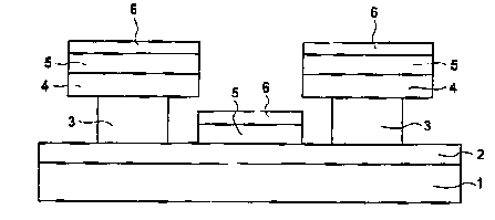
The figure shows, not to scale, a schematic cross section
through a method accord:ir.~g to the invention produced organic
light emitting diode. '~'h~ereby on a substrate 1 a transparent
structured bottom electrode 2 is located. The substrate,
which may comprise a non--planar geometry, Qf for example
2o glass, metal, silicon, or' polymer (in form of a foil); and the
bottom electrode is for example an ITO electrode (ITO = Indium
Tin Oxide). The subsequent layers include: a lower
photoresist layer 3; an upper photoresist layer 9; which i;a
integrated, and an active organic layer 5. On the organic
functional layer 5 the structured tvp electrode 6 (metal
electrode) is then positioned.
Example 1
Production of an OLED display
The production of a display proceeds accord~.n_g to the
following method steps:
1. An entire area of a glass sheet is coated with indium-tin-
oxide (ITO) and then structured according to a
photolithographic method (allowed by wet chemical. etching,
in such a way that parmllel conductor strips with a width of
approximately 200 l.~,m and a space of approximately 50 Eun are
CA 02335317 2000-12-15
DEC-14-00 16:31 +49 89 636 81720 P il R-150 Job-071
14-DEZ 2':16 DO VON:ZT PA 8 +49 85 636 8172e RN:613232844e SEITE:11
G!t 98 P 3429 P
formed. The photoresi.st used during structuring is them
completely removed. 'I~he conductor strips are each approx, 2
cm long and include at their outer ends additions for
external contacting it applicable,
5 2. The glass sheet will be heated approximately 1 hour at
temperature of Z50°C:, then a commercial photoresist on t:he
basis of polyglutarimide will be spun on (application for a
duration of 10 seconds at 700 rotations/minute, then spun
off for 30 seconds at 3000 rot:ations/minute). The received
io layer wi7.l be dried for 15 minutes at 150°C and then 30
minutes at 250°C in a ~~irculating air oven. A streaming
exposure at a wavelength of 248 nm (polychromatic) with a
dose of 100 mJ/cm' is created afterwards. Then a commercial
photoresist on the basis of Novolak/T)iazochinone (10:1
twinned with (1--mehtoxy-2-propyl)acetate) will be spun on at
2000 rotations/minute fox 20 seconds. Both layers will be
dried 60 seconds at 100°C, and afterwards with a radiation
dose of 62 mJ/cm' at a wave length of 365 nm (polychromatic)
via lithograph~.c: masking. Then with a commercial developer
which contains tetramethylammoniumhydroxyde, the structure
is developed for 20 seconds. Afterwards the glass sheet
will be put into a 100°C preheated air circulating oven and
annealed for 45 minutes at: 230°C; thereby cross,linking the
upper photoresist. Then the descrila~:d developer develops
twice more fox 70 ser_onds; thereby an overhanging of thE:
upper layer of approximately 5 dun is created. The layer
thickness of the lower layer i9 approximately 2,6~un; both
layers together are approx . ~ , 3 Eun thick . Af terwards , r~~s is t
remnants will be removed for 90 seconds from the TTO surface
3o by oxygen plasma (RF capacity: 70 W, gas f-lux: 30 sccm).
3. At a pressure of 10-6mhar, a layer of N,N~-(3methylpheyle)-
N,N'-(phenyl)-benzidin (m-'fPD) will be applied by
conventional vapor deposition (layer thickness: 135 nm,
deposition rate: 0,2 n:m/s).
4. Without the use of a mask, a 100 nm thick layer of magnesium
will be applied on the active surface of the display by
thermic deposition (de;Aosition rate: 1 nn~/5, pressure:l0-s
CA 02335317 2000-12-15
DEC'-14-00 16:37 +49 89 636 8172C'~ P 12 R-150 Jab-071
14-DEZ 2':16 DO VON:ZT PR 8 +49 89 636 81720 RN:6132328440 SEITE:12
GR 98 F X424 P
11
mbar). Interrupting t7ze vacuum, a 100 nm thick layer of
silver nm will be applied, also by vapor deposition, on the
active display area (deposition rate: 1 nm/s, pressure: 10'S
mbar). The resisting display flashes are clearly visibly in
the day light and the ~smission color is greenish-yellow.
Example 2
Production of a OLE17 display
A 1~ solvent of an electroluminescent polymer on >~.he basis of
fluorines in xylole is spun on (4000 rotations/min, 30 s) a
glass sheet with a produced layer build up corresponding to
example 1. Afterwards, i.t is dried for 60 seconds at B5°C.
1s Without the use of masking, a 100 nm thick layer of calcium
will be applied on the ar_tive area of the display by vapor
deposition (deposition r~ite_ 1nm/s, pressure: 10-Smbar).
Without interrupting the vacuum, a 100 nm thick layer of
silver will also be appl~~ed on the active display area by
vapor deposition (depoa:it:ion rate: 1 nm/s, pressure: 10-5mbar).
~fhe display flashes are clearly visibly in the day light and
the emission color is greenish-yellow-
CA 02335317 2000-12-15