Note: Descriptions are shown in the official language in which they were submitted.
CA 02335449 2000-12-18
FREE-STANDING AND ALIGNED CARBON NANOTUBES
AND SYNTHESIS THEREOF
This application claims the benefit of U.S. Provisional Patent
Application Serial No. 60/089,965, filed June 19, 1998, and U.S. Provisional
~ Patent Application Serial No. 60/099,708, filed September 10, 1998.
This invention was made through the support of the U.S. Army
Research Office (Grant No. DAAG55-97-1-0139). The Federal Government may
retain certain rights in the invention.
FIELD OF THE INVENTION
10 The present invention relates to a product with a substrate having
one or more carbon nanotubes, a method of producing that product, and devices
utilizing the product.
BACKGROUND OF THE INVENTION
Since the first observation of carbon nanotubes, numerous papers
15 have reported studies on the yield of well-graphitized nanotubes, their
diameter
and wall thickness (single or multiple), growth mechanisms, alignment,
electron
emission properties, nanodevices, theoretical predictions, and potential
applications. Selective positioning and growth of carbon nanotubes is
necessary
for future integration with conventional microelectronics as well as the
20 development of novel devices. However, limited progress has been reported
in
the controlled placement of nanotubes. Alignment of the carbon nanotubes is
particularly important to enable both fundamental studies and applications,
such
as cold-cathode flat panel displays, chargeable batteries, and vacuum
microelectronics.
25 Specifically, vertical alignment has been an important goal due to
its technological importance for applications such as scanning probe
microscopy
and field emission flat panel displays. Attempts to manipulate nanotubes for
these
applications have been made by post-growth methods such as cutting a polymer
resin-nanotube composite, or drawing a nanotube-ethanol suspension through a
30 ceramic filter. Because these techniques are difficult and labor intensive,
in situ
CA 02335449 2000-12-18
7 -
aligning of nanotubes during growth using techniques such as the nanopores of
porous alumina membranes and laser etched nanotracts have been attempted.
There has been little success in obtaining alignment of carbon
nanotubes on large areas until the report by Li et al., "Large-Scale Synthesis
of
Aligned Carbon Nanotubes," Science, 274:1701-1703 (1996) ("Li"). Li discusses
the growth of aligned carbon nanotubes on mesoporous silica containing iron
nanoparticles via thermal decomposition of acetylene gas in nitrogen gas at
temperatures above 700°C. In this method, the substrate is prepared by
a sol-gel
process from tetraethoxysilane hydrolysis in iron nitrate aqueous solution.
The
gel is then calcined 10 hours at 450°C at 10-2 Torr. A silica network
with
relatively uniform pores is obtained with iron oxide nanoparticles embedded in
the
pores. The iron oxide nanoparticles are then reduced at 550°C in 180
Torr of
flowing (9% HZ / N~ ( 110 cm3 / min) for 5 hours to obtain iron nanoparticles.
Thereafter, nanotubes are grown in a gas environment of a mixture of 9%
acetylene in nitrogen at 700°C. Aligned nanotube growth is along the
axial
direction of the pores. Only the nanotubes which grow out of the vertical
pores
are aligned. Nanotubes which grow from the iron particles on the surface and
in
the dispersed, inclined pores are random and non-oriented. In this method,
nanotube alignment is limited to the constraint of the vertically aligned
pores.
Further, the densiy and diameter of aligned carbon nanotubes is respectively
limited in direct proportion to the amount and size of the iron nanoparticles
and
the diameter of the pores.
As disclosed in Li, a temperature of at least 700°C is required to
decompose acetylene and induce carbon nanotube growth. Unfortunately, this
high temperature requirement limits substrate selection. For example, a glass
substrate is unsuited for use in this method due to its low strain point
temperature.
A glass produced by Corning Incorporated (Corning, New York) has the highest
known flat panel display glass deformation or strain point temperature of
666°C.
Typically, a commercially available flat panel display glass has a strain
point
temperature between 500°C and 590°C. At 700°C, glass
substrates deform and
inhibit aligned carbon nanotube growth. Accordingly, any substrate suitable
for
CA 02335449 2000-12-18
-3-
use with this method must have a melting point or strain point temperar_ure
above
700°C.
Terrones et al., "Controlled Production of Aligned-Nanotube
Bundles," Nature, 388: 52-55 (1997) ("Terrones") disclose a method for laser
induced growth of nanotube bundles aligned on a substrate under high
temperature conditions. A thin film of cobalt is deposited on a silica plate
b~- laser
ablation and thereafter etched with a single laser pulse to create linear
nanotracks.
2-amino-4,6-dichloro-s-triazine is then disposed onto the silica plate in the
presence of argon gas within a two stage oven. The first oven is heated to
10 1,000°C and then allowed to cool to room temperature. The second
oven is heated
to and maintained at 950°C. Although carbon nanotubes grow along the
edges of
the eroded nanotracks, growth only occurs on the substrate bottom surface and
in
a non-vertical fashion. Carbon nanotubes do not grow on a similarly prepared
substrate top surface which indicates nanotube growth according to this method
is
15 gravity dependent. Again, for the reasons discussed above, substrate
selection for
this method is limited to a substrate having either a strain point or melting
point
temperature above 1,000°C. Further, nanotube density is directly
limited to the
number of nanotracks etched into the substrate surface.
Thus. there remains a need for a method of forming aligned.
20 vertically or otherwise, carbon nanotubes at temperatures below
700°C.
Similarly, there remains a need for a substrate which has carbon nanotubes
vertically aligned on the substrate surface. Further, there remains a need for
a
method of forming individual, free-standing carbon nanotubes, and a substrate
with one or more individual, free-standing carbon nanotubes disposed on the
25 substrate surface. The present invention is directed to overcoming these
deficiencies in the art.
SUMMARY OF THE INVENTION
The present invention relates to a product which has a substrate and
either (1) a plurality of substantially aligned carbon nanotubes of a density
greater
30 than 104 nanotubes per square millimeter of substrate, (2) a plurality of
substantially aligned carbon nanotubes of a density no greater than 102
nanotubes
- CA 02335449 2000-12-18
-4-
per square millimeter of a substrate, (3) one or more carboy. nanotubes,
wherein
the substrate has a strain point or melting point temperature between about
300°C
and 700°C, (4) a plurality of substantially aligned carbon nanotubes
originating
and extending outwardly from the substrate outer surface, or (5) one or more
free-
standing carbon nanotubes originating and extending outwardly from the
substrate
outer surface.
Carbon nanotubes are synthesized by plasma-enhanced hot
filament chemical vapor deposition of a carbon source gas in a reduced
pressure
environment in the presence of a catalyst gas at temperatures as low as
between
10 300°C and 3000°C in a volume ratio range of carbon source gas
to catalyst gas
from 1: 2 to 1:10. Growth of large arrays of well-aligned carbon nanotubes
having a diameter between 4 to 500 nm occur on a substrate coated with a thin
metal catalyst film. Free-standing carbon nanotubes are grown on metal
catalyst
nano-dots disposed on the substrate.
1 ~ The present invention provides a method of forming aligned,
vertically or otherwise, carbon nanotubes at temperatures below 700°C.
Further,
products made in accordance with this method provide a substrate which has
carbon nanotubes vertically aligned on the substrate surface. Further, a
product
made in accordance with the method of the present invention includes a
substrate
20 having individual, free-standing carbon nanotubes. Still further, a product
made
in accordance with the method of the present invention includes a substrate
having
one or more individual, free-standing carbon nanotubes disposed on the
substrate
surface. Products of the present invention are useful in electrochemical
applications as well as in electron emission, structural composite, material
storage,
25 and microelectrode applications.
BRIEF DESCRIPTION OF THE DRAWINGS
Figures lA-B are scanned images showing alignment of carbon
30 nanotubes grown on a large-area of polycrystalline Ni substrates.
- - CA 02335449 2000-12-18
-5-
Figure 2 is a scanned image of a scanning electron microscope
micrograph of shom-ing carbon nanotubes grown at a higher plasma intensity
under the conditions listed in Table 1 (b).
Figure 3 is a scanned image showing carbon nanotubes with higher
S aspect ratios synthesized with a higher plasma intensity than that used for
the
carbon nanotubes shown in Figure 2.
Figure 4 is a scanned image showing a cluster of carbon nanotubes
scraped off a Ni substrate directly onto a Cu TEM grid, with the insert
showing a
cross-section image from a portion of a single mufti-walled carbon nanotube
10 structure.
Figures SA-B are scanned images showing carbon nanotubes
aligned substantially perpendicular to a substrate over large areas growth
conditions as listed in Table 2. Figure SB is an enlarged view of Figure SA
along
a peeled edge to show carbon nanotube diameters, length, straightness, and
1 S uniformity.
Figures 6A-C are scanned images showing scanning electron
microscope surface morphology of the nickel catalyst layers. Figure 6A
illustrates
the effects of NH3 plasma etching for 3 minutes. Figure 6B illustrates the
effects
of N~ plasma etching for 3 minutes. Figure 6C shows an as-sputtered smooth
20 catalyst surface.
Figures 7A-B are scanned images showing carbon nanotubes
grown under the conditions listed in Table 2. Figure 7B is an enlarged view of
Figure 7A to show carbon nanotube diameters and distributions.
Figure 8A is a scanned image showing thinner carbon nanotubes
25 grown on thinner ( 1 ~ nm) nickel-coated glass under the conditions listed
in Table
2. Figure 8B is a scanned image showing carbon nanotube with approximately 20
nm diameters grown under the conditions listed in Table 2.
CA 02335449 2000-12-18
-6-
Figures 9A-B are scanned images showing the interior and wall
structures of a typical thin carbon nanotubes, wherein Figure 9A is a cross-
section
view and Figure 9B is a plan view.
Figure 10 is a scanned image showing the large area growth of
5 well-aligned carbon nanotubes on glass.
Figure 11 is a scanned image showing well-aligned carbon
nanotubes on silicon.
Figure 12 is a scanned image showing very short carbon nanotubes
grown on silicon for only 2 minutes.
10 Figure 13 is a scanned image showing open ended carbon
nanotubes etched by HN03 for 1 minute.
Figure 14 is a scanned image showing carbon nanotubes subjected
to Ar ion sputtering.
Figure 15 is a scanned image showing a side view of well-aligned
15 carbon nanotubes grown at an angle with respect to the substrate.
Figure 16 is a scanned image showing a top view of the carbon
nanotubes of Figure 1 ~.
Figure 17A is a scanned image showing grown carbon nanotubes at
the edge of a metal pad. Figure 17B is a scanned image showing a region
similar
20 to Figure 17A in which the carbon nanotubes are broken.
Figures 18A-F are a series of scanned images displaying various
viewing angles of carbon nanotube obelisks grown from a patterned array of
catalyst nano-dots. Figure 18A is a perspective view of a plurality of
patterned
arrays. Figure 18B is a top view of the patterned arrays of Figure 18A at a
25 reduced magnification. Figure 18C is a perspective view of one patterned
array.
Figure 18D is a top view of one patterned array. Figure 18E is a perspective
view
- CA 02335449 2000-12-18
- 7
at an increased magnification of the patterned array of Figure 18C. Figure 18F
is
a perspective view of spaced-apart carbon nanotube obelisks.
Figure 19 is a scanned image showing an elevation view of a
carbon nanotube obelisk.
5 Figure 20 is a partial, top view of a field emission display
apparatus of the present invention.
Figure 21 is a perspective view of a probe for a scanning electron
microscope of the present invention.
Figure 22 is a schematic illustrating an example of a scanning
10 electron microscope of the present invention.
Figure 23 is a schematic drawing illustrating an example of the
basic construction of a battery of the present invention.
Figure 24 is a schematic drawing illustrating a fuel cell of the
present invention.
15 Figure 25 is a schematic drawing illustrating an electromagnetic
interference shield disposed between an electromagnetic interference source
and
an electronic component.
Figure 26 is a schematic drawing illustrating a microelectrode of
the present invention.
20
DETAILED DESCRIPTION OF THE INVENTION
The present invention relates to a product which includes a
substrate and one or more hollow core carbon nanotubes originating from a
surface of the substrate. When the product has more than one carbon nanotube,
25 the carbon nanotubes are well-aligned and may lie on or extend either
perpendicularly or non-perpendicularly from the substrate surface. Embodiments
of the product of the present invention include the substrate and either (1 )
a
_ - CA 02335449 2000-12-18
g _
plurality of substantially aligned carbon nanotubes of a density greater than
10~
nanotubes per square millimeter of substrate, (2) a plurality of substantially
aligned carbon nanotubes of a density no greater than 102 nanotubes per square
millimeter of a substrate, (3) one or more carbon nanotubes, wherein the
substrate
5 has a strain point or melting point temperature between about 300°C
and 700°C,
(4) a plurality of substantially aligned carbon nanotubes originating and
extending
outwardly from the substrate outer surface, or (5) one or more free-standing
carbon nanotubes originating and extending outwardly from the substrate outer
surface.
As shown in Figures 1-19, carbon nanotubes of the present
invention are substantially concentric tubules. The nanotubes have diameters
ranging from 4 to 500 nm and lengths up to 50 Vim. Preferably, carbon
nanotubes
which are longer than 20 ~m have a diameter of at least 50 nm to maintain
alignment. Depending upon growth conditions, the carbon nanotubes can be
15 either free-standing nanotube obelisks which have a sharp, tapered carbon
tip or a
large array of well-aligned nanotubes which have a cap distally located from
the
substrate. The large arrays of carbon nanotubes have densities of 106 to 10g
nanotubes per square millimeter of substrate. The cap comprises a catalyst
metal
or metal alloy material of iron, cobalt, nickel, or an alloy of iron, cobalt,
or nickel.
20 The catalyst material and its role is discussed further below. In an
embodiment of
the present invention, the tips and caps are removed to reveal open-ended
carbon
nanotubes.
It is contemplated that a wide variety of electrically or non-
electrically conductive substrates can be utilized with the present invention.
For
25 example, suitable substrates include glass, silica, quartz, silicon,
platinum, iron,
cobalt, nickel, an alloy of iron, cobalt, or nickel, a ceramic, or a
combination
thereof. Particularly useful substrates are glass panels and silicon wafers.
It is
important to recognize that the most important property of the substrate is
that the
substrate strain point and/or melting point temperatures are above the
temperature
30 of carbon nanotube growth. With the present invention, the substrate must
have
strain point and/or melting point temperatures of at least about 300°C.
As
disclosed in Li, substrates utilized in the prior art must have strain point
and/or
melting point temperatures in excess of 700°C. Accordingly, a product
of the
CA 02335449 2000-12-18
-9-
present invention and the substrate therein have a strain point or melting
point
temperature between 300°C and 700°C. Such substrates include
flat panel display
glass substrates, which have strain point and/or melting point temperatures of
666°C and below. may be utilized. Certain ceramics, such as LaAl03,
AlzO;, and
5 Zr02, YSZ. and SrTi03 have melting point temperatures of about 3000°C
and are
useful as substrates utilized in high temperature environments.
In the present invention, carbon nanotubes are uniquely grown on
a surface of a substrate by providing the substrate in a reduced pressure
environment containing a carbon source gas and a catalyst gas and exposing the
10 substrate to a plasma under conditions effective to cause formation and
growth of
one or more carbon nanotubes on the substrate. This is defined as plasma-
enhanced hot filament chemical vapor deposition (PE-HF-CVD). Accordingly,
the present invention is also directed to products which have carbon nanotubes
originating and extending outwardly from an outer surface of the substrate.
15 Prior to growing the carbon nanotubes by PE-HF-CVD, the
substrates are placed into a deposition chamber at a reduced pressure (< 6 x
10'6
Torr ) and coated with the catalyst metal or_metal alloys discussed above.
Either a
metal catalyst film of at least about 15 nm thick or one or more metal
catalyst
nano-dots of about 1 SO~r thick is deposited onto the substrate. The catalyst
film is
20 deposited by radio frequency magnetron sputtering. The catalyst nano-dots
are
deposited by electron beam evaporation, thermal evaporation, or magnetron
sputtering. Surprisingly, the resultingly grown carbon nanotube diameters are
directly related to the thickness of the catalyst film. By varying the
thickness of
the catalyst film, the diameter of the carbon nanotubes can be controlled.
25 Although nano-dot thickness can have a like effect on resulting nanotube
diameter, the thickness is less controlling as the film.
To produce the products of the present invention, the coated
substrates are placed into a reduced pressure CVD chamber containing a carbon
source gas and a catalyst gas and are then exposed to a plasma under
conditions
30 effective to cause formation and growth of one or more carbon nanotubes on
the
substrate surface. Generally, the CVD chamber has a pressure between about 0.1
to about 100 Torr, preferably about 1 to about 20 Ton. Because carbon nanotube
growth is induced by plasma enhanced chemical vapor deposition of the carbon
CA 02335449 2000-12-18
-10-
source gas, the heated environment of the CVD chamber can be maintained at a
temperature between about 300°C and about 3000°C. As a result of
the low
temperature requirement, various substrates having relatively low strain point
or
melting point temperatures as low as about 300°C may utilized in the
present
5 invention. As indicated above, carbon nanotubes growth may occur at vent
high
temperatures and is only constrained by the melting point temperature of the
selected substrate. The upper temperature limit of carbon nanotube growth is
estimated to be about 3000°C, which corresponds to the highest known
ceramic
substrate melting point temperature, as discussed above. The growth time
10 depends on the requirement of nanotube length. Normally, it is between 1 -
10
minutes, which yields a length of 0.1 - 20 um. Growth durations can extend up
to
5 hours depending on the desired carbon nanotube lengths.
The carbon source and catalyst gases flow through the CVD
chamber with a volume ratio of carbon source gas to catalyst gas ranging from
1:
15 2 to 1:10 at a maintained pressure between about 0.1 to about 100 Torr at a
temperature between about 300°C to 3000°C. The carbon source gas
may be
selected from saturated or unsaturated linear, branched, or cyclic carbon and
hydrogen compounds having up to six carbon atoms which are gases at the
deposition pressure. For example, very pure (99.99% purity) acetylene,
ethylene,
20 and benzene, preferably acetylene, may be utilized as the carbon source gas
of the
present invention. The catalyst gas is ammonia (99.99% purity) at CVD
temperatures below 700°C. At CVD temperatures above 700°C, the
catalyst gas
may be ammonia. nitrogen (99.99% purity), or a combination thereof. Ammonia
is the preferred catalyst gas of the present invention. Preferably, the carbon
25 source and catalyst gases are introduced into the CVD chamber
simultaneously or
the catalyst gas is introduced prior to the carbon source gas.
Carbon nanotubes are synthesized with the diameter, length, site
density, and growing angle controlled. Plasma intensity may be varied to
determine the nanotube aspect ratios for diameter and length, and range of
both
30 site and height distributions. Vertical or non-vertical growth of the
carbon
nanotubes is independent of the substrate surface topography and can be
controlled by the angle placement of the substrate in the CVD chamber with
respect to the orientation of the electric field of the plasma generator.
CA 02335449 2000-12-18
-11-
These lower temperature growth conditions are suitable for
electron emission applications, such as cold-cathode flat panel displays which
require the carbon nanotube emitters to be grown substantially perpendicular
to a
glass substrate surface. However, carbon nanotubes grown at the lower
5 temperatures have more wall defects or discontinuations. These
discontinuations
provide a diffusion path to the nanotube core. Should there be a desire to
manufacture carbon nanotubes with limited defects, higher growth temperatures
may be utilized.
The Growth mechanism of aligned carbon nanotubes is ascribed in
10 the literature to be a constraint of either the pores in mesoporous silica
or the laser
etched tracks in silica. In the present invention, the alignment of the carbon
nanotubes cannot be due to pores or etched tracks since there are no pores or
etched tracks in the glass substrates, as shown in Figures SA-B, 10, 15, 17A-
B,
and 18C, E, and F. Rather, alignment is due to a nanotube nucleation process
1 S catalyzed by the catalyst gas (e.g., ammonia) and the catalyst layer or
nano-dot
(e.g., nickel). In the presence of the catalyst gas, each metal catalyst cap
efficiently catalyzes the continuous synthesis of carbon nanotubes. With the
growth of the carbon nanotubes, the cap is maintained at the distal end of
each
carbon nanotube. The alignment and thickness of the carbon nanotubes may be
20 determined by the orientation and size respectively of the initial
catalytic centers.
If desired, the catalyst metal caps can be removed by subjecting the carbon
nanotubes to either HN03 solution etching or Ar ion sputtering to open the
distal
ends.
In some applications, a single carbon nanotube or patterns with
25 controlled site density is desired, which can be accomplished by selective
deposition of the catalyst nano-dots. In the present invention, the carbon
nanotubes grown from the metal catalyst nano-dots are obelisks which have
tapered, sharp carbon tips and have rounded base diameters approximately the
same as the nano-dots. The nanotube height depends on the growth time and
30 nano-dot thickness. The tips can be removed as well to provide an open
ended
nanotube by placing the nanotubes in a reaction chamber and exposing the
nanotubes to oxygen and heat at about 400°C for about 0.5 hour.
CA 02335449 2000-12-18
-12_
A filling can be placed within the carbon nanotubes through the
open ends or through the structural discontinuations. For example, fillings
such as
hydrogen, lithium ions, bismuth, lead telluride, bismuth tritelluride, or a
pharmacological agent, to name only a few, may be inserted into the nanotube
core by electrochemical or physical methods. If desired, the open ends of the
carbon nanotubes can be enclosed or sealed by magnetron sputtering or
electrochemical deposition of an enclosing material, such as a metal.
Now, referring to Figure 20, a conventional flat panel display or
field emission display 100 has a baseplate 102, a spaced-apart phosphor coated
faceplate 104, and an electron emitter array 106 positioned on the baseplate
102
for emitting electrons to impinge upon and thereby illuminate the phosphor
coating. The baseplate 102, the faceplate 104 and the emitter array 106 are
disposed in a vacuum environment. The emitter 106, which is operably connected
to an electron generating source, has a sharp tip 108, known as a Spindt tip,
to
1 ~ emit electrons. However, these emitters 106 have certain drawbacks because
they
have a relatively short wear life, have a low emission density due to the
limits of
existing lithography technology, and are relatively expensive. Products of the
present invention comprising large arrays of well-aligned carbon nanotubes as
shown in, for example, Figures l, 2, 5, 7, 10, 1 l, and 18B, can be used to
replace
the base plate/emitter array combination 102 and 106. Since the carbon
nanotubes
can be produced highly aligned and perpendicular to the substrate, field
emission
displays can be fabricated utilizing such arrays as emitters. Further, as
discussed
in Schmid et al., "Carbon Nanotubes Are Coherent Electron Sources," Appl.
Phys.
Lett., 70(20):2679-2680 (1997)("Schmid"), Collins et al., "A Simple And Robust
2~ Electron Beam Source From Carbon Nanotubes," ADpI. Phys. Lett., 69(13):1969-
1971 (1996), and Rinzler et al., Unraveling Nanotubes: Field Emission From an
Atomic Wire," Science, 269: 1550-1553 (1995) ("Rinzler"), all of which
incorporated herein by reference, carbon nanotubes emit electrons in the same
manner as the Spindt tips upon operable connection to an electron generating
30 source. Not only can the carbon nanotubes increase emitter wear life,
contrast and
brightness are improved as well due to the large nanotube density.
Referring to Figures 19, 21, and 22, and generally to Figures 1-18, the
products of the present invention can be utilized as a probe for a scanning
electron
'-- CA 02335449 2000-12-18
-13-
microscope, as indicated in Rinzler. A scanning electron microscope 200 of the
present invention comprises a vacuum chamber 202 capable of receiving a
specimen 204, an electron source 206 for producing electrons, a probe 208
which
is operably positioned within the vacuum chamber 202 for emitting and
directing
the electrons toward and scanning the specimen 204, a detector 210 operably
positioned within the vacuum chamber 202 for collecting radiation issuing from
the specimen 204 as a result of scanning by the probe 208 to produce an output
signal, and a display screen 212 operably connected to the detector 210 to
receive
the output signal and resulting display an image of the area of the specimen
204
10 scanned by the probe 208. Referring to Figures 1-SB, 7-19 and 21, the probe
208
is a product of the present invention having a substrate and either ( 1 ) a
plurality of
substantially aligned carbon nanotubes of a density greater than 104 nanotubes
per
square millimeter of substrate; (2) a plurality of substantially aligned
carbon
nanotubes of a density no greater than 10z nanotubes per square millimeter of
a
15 substrate; (3) one or more carbon nanotubes, wherein the substrate has a
strain
point or melting point temperature between about 300°C and
700°C; (4) a
plurality of substantially aligned carbon nanotubes originating and extending
outwardly from an outer surface of the substrate; or (5) one or more free-
standing
carbon nanotubes originating and extending outwardly from an outer surface of
20 the substrate. Preferably, the probe 208 is a product of the present
invention
comprising a substrate 214 having an outer surface 216 and one free-standing
carbon nanotube 218 originating and extending from the outer surface 216 of
the
substrate 214.
Selective positioning and growth of a single, free-standing carbon
25 nanotube from a single, catalyst nano-dot in accordance with the method of
the
present invention as previously described can produce the probe 208. Referring
to
Figure 21, and generally to Figure 19, a single, free-standing carbon nanotube
218
originating and extending from an outer surface 216 of a substrate 214 is
operably
connected to the electron source 206. The substrate 214 is selected from an
30 electrically conductive material, which is connectable to the electron
source.
In operation, the specimen 204 is positioned within the vacuum
chamber 202, and the chamber 202 is evacuated. The microscope 200 scans the
specimen 204 with a fine probe of electrons emitting from the probe 208. The
_ - CA 02335449 2000-12-18
- 14-
electrons are produced from the electron source 206, which can be a field-
emission electron source (not shown) and suitable accelerating electrodes (not
shown), such as an electron gun (not shown). Electrons that are transmitted
through the specimen 204 are collected by the detector 210 to provide the
output
5 signal. For example, the detector 210 can comprise a phosphor screen (not
shown) with a photomultiplier (not shown) for detecting light from the screen.
This output signal is used to modulate the beam of the display screen 212,
such as
a cathode ray tube, which is scanned in synchronism with the probe 208, so as
to
cause the display screen 212 to display a pattern which depends on the
structure of
10 the scanned portion of the specimen 204. Alternatively, instead of
collecting
transmitted electrons, secondary radiation (e.g., electrons or x-rays),
emitted from
the specimen 204 as a result of bombardment by the electrons of the probe 208,
may be detected to provide the output signal.
In such a microscope, the electron fine probe or carbon nanotube
15 218 must be very fine, such as to illuminate only a small region of the
specimen
204, in order to enable small features of the specimen 204 to be examined.
Production of a fine probe of electrons requires an electron source 206 having
a
very small electron-emitting area such as, for example, a field-emission
electron
source. Magnets 220 can be operably disposed in the vacuum chamber 202 to
20 focus or alter the emitted electron probe. Carbon nanotubes produced in
accordance with the present invention are such electron emitters.
The products of the present invention can also be utilized to form
alkali metal ion batteries, such as, lithium batteries. As shown in Figure 23,
the
battery 300 comprises an anode 302, a cathode 304, an insulator 306 disposed
25 between the anode 302 and the cathode 304, and an electrolyte 308. At least
one
of the anode 302 and the cathode 304, preferably both, comprise a product of
the
present invention having a substrate and either (1) a plurality of
substantially
aligned carbon nanotubes of a density greater than 104 nanotubes per square
millimeter of substrate; (2) a plurality of substantially aligned carbon
nanotubes of
30 a density no greater than 102 nanotubes per square millimeter of a
substrate; (3)
one or more carbon nanotubes, wherein the substrate has a strain point or
melting
point temperature between about 300°C and 700°C; (4) a plurality
of substantially
aligned carbon nanotubes originating and extending outwardly from an outer
CA 02335449 2000-12-18
-15-
surface of the substrate; or (5) one or more free-standing carbon nanotubes
originating and extending outwardly from an outer surface of the substrate.
Preferably, the product has a plurality of substantially aligned carbon
nanotubes of
a density greater than 104 nanotubes per square millimeter of substrate.
Here. the substrate comprises an electrically conductive material,
and the carbon nanotubes have at least one diffusion path to the hollow core
of the
nanotubes. As reported in Gao et al, "Electrochemcial Intercalation of Single-
walled Carbon Nanotubes with Lithium," Chem. Phvs. Lett., (in press) ("Gao")
alkali metals can be electrochemically intercalated into the hollow cores of
carbon
10 nanotubes. Gao also reports that lithium can be reversibly intercalated
from the
nanotubes in the range of 100-400 mAh/g. In the present invention, lithium
ions
may be intercalated into the carbon nanotubes of the anode 302 by charging the
battery 300.
Although not required, the carbon nanotubes of the product may
15 have open ends to provide the metal diffusion path, as shown in Figure 13.
Preferably, the carbon nanotubes have high structural defect or
discontinuation
densities in the walls. As previously discussed, carbon nanotubes grown at low
growth temperatures (e.g., 300°C to 400°C) by PE-HF-CVD have
such structural
discontinuations. These structural discontinuations provide high active
surface
20 areas and numerous diffusion paths to the nanotube core for metal
diffusion. It is
not necessary for the carbon nanotubes having discontinuations to be open-
ended,
since most metal diffusion occurs through the discontinuations.
In the present invention, the cathode 304 functions to assist
conduction for collecting current, and the anode 302 functions as the host
material
25 for the lithium ions. Since the anode 302 and/or the cathode 304 comprises
well-
aligned carbon nanotubes, the electrolyte 308 easily permeates the nanotubes,
which act as electrodes. As a result, impedance of the battery 300 is
decreased,
the charge-discharge efficiency is improved over conventional batteries, and
secondary reactions during charge and discharge are prevented. Thus, the
battery
30 300 of the present invention has a high capacity and a long life cycle.
When the cathode 304 comprises the product of the present
invention having intercalated lithium ions, a higher collecting ability can be
CA 02335449 2000-12-18
- 16-
attained. As a result. the utilization of the cathode 304 can be increased to
produce a high-capacity lithium battery 300.
Products of the present invention having carbon nanotubes
substantially aligned and oriented substantially perpendicular with respect to
the
substrate are preferred. By utilizing such products, the electrolyte 308 can
permeate the nanotubes much easier. This results in the battery 300 being
capable
of rapid charge and discharge. In the anode 302, lithium can be deposited on
the
carbon nanotubes surfaces and intercalated into the nanotubes, thereby
preventing
the growth of dendritic lithium metal deposition and resulting in the battery
300
10 having a higher capacity. Also, when the products of the present invention
are
used as an anode 302 for intercalating and deintercalating lithium ions, a
high-
capacity anode 302 is formed.
Again referring to Figure 23, the anode 302 and the cathode 304
are disposed in the electrolyte 308 held in a housing 310 opposite to each
other
1 ~ through the insulator 306. The insulator 306 is provided for preventing
internal
shorts due to contact between the anode 302 and the cathode 304. The anode 302
and the cathode 304 respectively can comprise the products shown in Figures 1-
19. An anode terminal 312 and a cathode terminal 314 are electrically
connected
to the respective product substrates comprising the anode 302 and the cathode
?0 304. The anode terminal 312 and the cathode terminal 314 may be utilized
for at
least a portion of the housing 310. When a lithium battery 300 of the present
invention is assembled, the anode 302 and cathode 304 must be sufficiently
dehydrated and dried. For example, dehydration can be performed by heating
under reduced pressure.
The carbon nanotubes serve as the collecting electrodes of the
anode 302 and the cathode 304. The nanotubes function to efficiently supply a
current to be consumed by electrode reaction during charge and discharge or to
collect the current generated by the electrode reaction.
The insulator 306 functions to prevent internal shorts between the
30 anode 302 and the cathode 304, and can function to hold the electrolyte
308. The
insulator 306 must have pores which permit movement of lithium ions, and must
be insoluble and stable in the electrolyte 306. Thus, examples of materials
which
may be used for the insulator 306 include glass, polyolefins, such as
CA 02335449 2000-12-18
-17-
polypropylene and polyethylene, fluororesins, and materials having a micropore
and nonwoven fabric structure. A metal oxide film having micropores and a
resin
film compounded with a metal oxide can also be used.
An electrolyte solution is prepared by dissolving the electrolyte
5 308 in a solvent. Examples of electrolytes 308 include acids, such as HZSO~,
HC1" and HN03, salts comprising lithium ions and Lewis acid ions (BF4-, PF6 ,
C104~, CF3S03-, and BPh4-), and salt mixtures thereof. Salts comprising canons
such as sodium ion, calcium ion , and tetraalkylammonium ion, and the Lewis
acid ions can also be used. These salts can be sufficiently dehydrated and
10 deoxidized by heating under reduced pressure.
Examples of solvents which are useful for the electrolyte 308
include acetonitrile, benzonitrile, propylenecarbonate, ethylenecarbonate,
dimethylcarbonate, diethylcarbonate, dimethylformamide, tetrahydrofuran,
nitrobenzene, dichloroethane, diethoxyethane, 1,2-dimethoxyethane,
15 chlorobenzene, gamma -butyrolactone, dioxolan, sulfolan, nitromethane, 2-
methyltetrahydrofuran, 3-propylsydnone, sulfurdioxide, phosphorylchloride,
thionylchloride, sulfurylchloride, and solvent mixtures thereof. These
solvents
can be dehydrated by activated alumina, molecular sieves, phosphorus
pentaoxide,
or calcium chloride. Some of the solvents are also subjected to removal of
20 impurities and dehydrated by distillation in coexistence with an alkali
metal in an
inert gas.
To prevent electrolyte 308 leakage, the electrolyte 308 can be
formed into a gel. Polymers which absorb the solvent of the electrolyte 308
and
swell may be used as a gelling agent. For example, such polymers include
25 poly(ethyleneoxide), poly(vinylalcohol), polyacrylamide, and the like.
The products of the present invention may be utilized to form fuel
cells. A fuel cell is a device for directly converting the chemical energy of
a fuel
into electrical energy. There are various constructions of fuel cell devices,
such as
fuel cells, fuel cell groups or stacks, and fuel cell power plants which use
30 hydrogen as the fuel for the respective fuel cell device. As is well known,
an
exothermic chemical reaction takes place in these fuel cell devices between
hydrogen and an oxidant, for example, oxygen, resulting in the formation of
water
as the reaction product and the desired generation of electricity. The
incidental
CA 02335449 2000-12-18
-18-
release of thermal energy exhibited as sensible heat is typically removed from
the
fuel cell. During the above reaction, hydrogen and the oxidant are consumed by
the fuel cell. For the fuel cell device to continue its operation, hydrogen
and the
oxidant must be replenished at their respective consumption rates.
In some fuel cell applications, hydrogen is stored in tanks or
similar containers in its liquid or gaseous state in its pure form or in
combination
with inert substances. However, such containers are generally relatively large
and
heavy, and problematic when storage space and/or payload weight are limited.
Thus, there is an advantage when large amounts gaseous hydrogen can be stored
10 in compact, relatively light weight containers.
Referring to Figure 24, a fuel cell 400 of the present invention
comprises a housing 402, two gas diffusion electrodes, an anode 404 and a
cathode 406, positioned within the housing 402 and respectively forming an
anode
side 408 and a cathode side 410, an electrolyte impregnated matrix or ion
15 exchange membrane 409 positioned between and in electrical contact with the
electrodes 404 and 406, an external circuit 412 electrically and operably
connecting the anode 404 to the cathode 406 and a hydrogen storage unit 414
comprising products 416 of the present invention positioned within an
enclosure
418 which is operably connected to the anode side 408. A catalyst layer is
20 disposed on the electrolyte-facing surfaces of the respective electrodes
404 and
406. In the operation of the fuel cell 400, hydrogen gas is fed to the back
side of
the anode 404, and oxygen gas is fed to the back side of the cathode 406. The
respective gases diffuse through the electrodes 404 and 406 and react at the
catalyst sites to yield electrical energy, heat, and moisture.
25 On the anode side 408 of the fuel cell 400, hydrogen is
electrochemically oxidized to give up electrons in accordance with the
reaction:
2H2 -~ 4H+ + 4e-. The electrical current so generated is conducted from the
anode
404 through the external circuit 412 to the cathode 406. On the cathode side
410
of the fuel cell 400. the electrons are electrochemically combined with the
oxidant
30 in accordance with the reaction: 02 + 4H+ + 4e ~ 2 HZO. The related flow of
electrons through the electrolyte completes the circuit.
Referring additionally to Figures 1-19, the hydrogen storage unit
414 comprises the enclosure 418 and products 416 of the present invention
having
- CA 02335449 2000-12-18
- 19-
a substrate and either ( 1 ) a plurality of substantially aligned cap bon
nanotubes of a
density greater than 104 nanotubes per square millimeter of substrate; (2) a
plurality of substantially aligned carbon nanotubes of a density no greater
than l Oz
nanotubes per square millimeter of a substrate; (3) one or more carbon
nanotubes,
wherein the substrate has a strain point or melting point temperature between
about 300°C and 700°C; (4) a plurality of substantially aligned
carbon nanotubes
originating and extending outwardly from an outer surface of the substrate; or
(5)
one or more free-standing carbon nanotubes originating and extending outwardly
from an outer surface of the substrate. The carbon nanotubes have a hollow
core
10 and at least one diffusion path into the core. Preferably, the product 416
has
plurality of substantially aligned carbon nanotubes of a density greater than
104
nanotubes per square millimeter of substrate with a high discontinuation
density in
the nanotube structure to provide a plurality of diffusion paths. Further, the
carbon nanotubes of this product 416 can have an open end distal from the
1 ~ substrate. Particularly useful are single-walled carbon nanotubes of the
present
invention which have a diameter of 1 nm. These nanotubes form bundles and are
strong hydrogen gas absorbers. Hydrogen can be introduced into the carbon
nanotube hollow core by placing the product 416 in a high pressure chamber
(not
shown) and introducing hydrogen gas at relatively high pressures into the
chamber
20 to diffuse hydrogen across the diffusion paths into the carbon nanotubes.
Also,
hydrogen can be diffused into the nanotubes electropotentially or
electrochemically. Further, heated products 416 can be placed into a hydrogen
rich environment and allowed to cool, thereby drawing hydrogen into the
nanotubes. Because the light-weight carbon nanotubes of the present invention
25 have relatively large cores and surface areas, large amounts of hydrogen
can be
stored therein.
The products of the present invention can also be utilized to form
composites with other dissimilar materials. Suitable dissimilar materials
include
metals, ceramics, glasses, polymers, graphite, and mixtures thereof. Such
30 composites are prepared by coating the products of the present invention
with
these dissimilar materials in solid particulate form or in liquid form.
A variety of polymers, including thermoplastics and resins, can be
utilized to form composites with the products of the present invention. Such
CA 02335449 2000-12-18
-20-
polymers include, for example, polyamides, polyesters, polyethers,
polyphenylenes, polysulfones, polyurethanes, or epoxy resins.
In another embodiment, the composite contains an inorganic
material. e.g., a ceramic material or a glass. For example, a high-temperature
5 copper oxide superconductor ceramic materials, such as BiSrCaCuO (BSCCO),
TIBaCaCuO (TBCCO), Bi2Sr2CaCu20g (Bi-2212), Bi2Sr2Ca2Cu30,o (Bi-2223).
TI~Ba~Cu06 (Tl-2201), TIzBaZCaCu208 (Tl-2212), T12Ba2Ca2 Ca2Cu301o (Tl-
2223). TIBa~CaCu20~ (1212), TlBa2CaZCu309 (Tl-1223), and any ceramic
composition derived from these compositions, such as partial replacement of Tl
by
10 Bi, Pb. Bi, or Pb, Ba by Sr, and Ca by Y or Cr., are useful in the present
invention.
These ceramics are deposited on the products of the present invention by
magnetron sputtering, laser ablation, thermal spraying, electron beam
evaporation,
etc. to coat the substantially perpendicular, aligned carbon nanotubes an form
a
high temperature superconducting material. Due to the high degree of nanotube
15 alignment, excellent magnetic flux line core-pinning interaction can be
obtained to
enhance critical current densities (J~) without destroying an unnecessary
volume
fraction of the superconductor.
As discussed in Yang et al., "Nanorod-Superconductor
Composites: A Pathway to Materials with High Critical Current Densities,"
20 Science, 273: 1836-1840 (1996), incorporated herein by reference, large-
scale
applications of the high-temperature copper oxide superconductor ("HTSC")
materials listed above require high J~ at temperatures near the boiling point
of
liquid nitrogen to be technologically useful. By inserting columnar defects
into
the HTSC materials. high J~ can be maintained at higher temperatures when
25 subjected to an electric current. The columnar defects can be accomplished
by
coating products of the present invention with the HTSC materials.
Accordingly,
a high temperature superconductor comprises a product having a substantially
non-electrically conductive substrate and either (1) a plurality of
substantially
aligned carbon nanotubes of a density greater than 104 nanotubes per square
30 millimeter of substrate; (2) a plurality of substantially aligned carbon
nanotubes of
a density no greater than 102 nanotubes per square millimeter of a substrate;
(3)
one or more carbon nanotubes, wherein the substrate has a strain point or
melting
point temperature between about 300°C and 700°C; (4) a plurality
of substantially
CA 02335449 2000-12-18
-21 -
aligned carbon nanotubes originating and extending outwardly from an outer
surface of the substrate; or (5) one or more free-standing carbon nanotubes
originating and extending outwardly from an outer surface of the substrate, a
high-
temperature copper oxide superconductor material in admixture with the
product,
and at least two spaced apart terminals connectable to an electric circuit,
whereby
the product and the high-temperature copper oxide superconductor material
admixture are subjectable to an electric current.
In still another embodiment, the composite includes a metal.
Suitable metals include aluminum, magnesium, lead, zinc, copper, tungsten,
10 titanium, niobium, hafnium, vanadium, and alloys thereof.
Referring to Figure 25 and generally to Figures 1-5B and 7-19, an
electromagnetic interference (EMI) shield 500 is formed from a product of the
present invention comprising a substrate and either ( 1 ) a plurality of
substantially
aligned carbon nanotubes of a density greater than 104 nanotubes per square
15 millimeter of substrate; (2) a plurality of substantially aligned carbon
nanotubes of
a density no greater than 102 nanotubes per square millimeter of a substrate;
(3)
one or more carbon nanotubes, wherein the substrate has a strain point or
melting
point temperature between about 300°C and 700°C; (4) a plurality
of substantially
aligned carbon nanotubes originating and extending outwardly from an outer
20 surface of the substrate; or (5) one or more free-standing carbon nanotubes
originating and extending outwardly from an outer surface of the substrate and
a
dissimilar material in admixture with the product. The dissimilar material
comprises a polymer. graphite, or a combination thereof . Such polymers are
thermoplastics and resins and can include, for example, polyamides,
polyesters,
25 polyethers, polyphenylenes, polysulfones, polyurethanes, or epoxy resins.
The
electromagnetic interference shield 500 is operationally positioned with
respect to
either an electromagnetic source 502 or an electronic component 504.
The composite can be used as an EMI shielding material in the
construction of gaskets, housings for electronic components, including
30 components within computers, conducting cables, and shielded rooms, EMI
emission sources 502, and other applications known in the art. Depending upon
the substrate selected for the product, such an EMI shield 500 is particularly
useful in high temperature environments. In a process for shielding an
electronic
CA 02335449 2000-12-18
-22-
component X04 against EMI produced by the electromagr~eiic radiation source
502, the EMI shield 500 of the present invention is interposed between the
electronic device X04 and the electromagnetic radiation source 502.
Interference
of the device 504 by the radiation source 502 is thereby substantially reduced
or
5 eliminated. A shielded electronic component 504 for resisting EMI generated
by
the electromagnetic source 502 has an electronic component X04 and a EMI
shield
500 of the present invention operatively positioned with respect to the
component
504. A shielded electromagnetic emission source 502 has an EMI emitting source
502 and EMI shield 500 of the present invention operatively positioned with
10 respect to the source 502.
Still. the products of the present invention can as well be utilized to
form a microelectrode 600, as shown in figure 26 and discussed in Stulik et
al.,
"Microelectrodes: Definitions, Characterization and Hints For Their Use,"
IUPAC Commission, 5: Document No. 550/61/97 (1999), incorporated herein by
15 reference. The microelectrode 600 comprises a product having a
substantially
non-electrically conductive substrate 602 and either (1) a plurality of
substantially
aligned carbon nanotubes 604 of a density greater than 104 nanotubes per
square
millimeter of substrate; (2) a plurality of substantially aligned carbon
nanotubes
604 of a density no greater than 102 nanotubes per square millimeter of a
20 substrate; (3) one or more carbon nanotubes 604, wherein the substrate 602
has a
strain point or melting point temperature between about 300°C and
700°C; (4) a
plurality of substantially aligned carbon nanotubes 604 originating and
extending
outwardly from an outer surface of the substrate 602; or (5) one or more free-
standing carbon nanotubes 604 originating and extending outwardly from an
outer
25 surface 606 of the substrate 602 and at least one electrically conductive
microfiber
608 operably connected to at least one carbon nanotube 604 of the product,
wherein the at least one carbon nanotube 604 is operably and electrically
connectable to an electric circuit.
Particularly well suited for use as an electrode or an array of
30 electrodes are carbon nanotubes having open ends, as shown in Figure 13.
The
carbon nanotubes are grown on a non-electrically conductive substrate, such as
glass, quartz, or a ceramic. The carbon nanotubes are operably and
electrically
CA 02335449 2000-12-18
- 23 -
connectable to an electric circuit with electrically conductive microfibers,
such as.
platinum or carbon microfibers, attached to the nanotubes.
EXAMPLES
5
Example 1
Polished polycrystalline and single-crystal Ni substrates were
placed into a chemical vapor deposition (CVD) chamber, and the pressure was
reduced to < 6 x 10⁻⁶ Torr. Acetylene gas (99.99 % purity) and ammonia gas
10 (99.99 % purity) were introduced into the chamber at a total flow rate of
120-200
standard cm3 per minute (sccm) and at a maintained working pressure of 1-20
Ton under the conditions listed in Table 1. After stabilizing the working
pressure,
a tungsten filament coil powered by a DC source (a 0-500 V DC, 3 A power
supply, Advanced Energy MDX 1.5K-magnetron drive) and a plasma-generator
1 ~ were energized to generate heat and plasma at a temperature below
666°C to
induce carbon nanotube growth. Samples of the carbon nanotubes were examined
by scanning electron microscopy (SEM, Hitachi S-4000) to measure tube lengths,
diameters, site distributions, alignment, density and uniformity. High-
resolution
transmission electron microscopy (TEM) was used to determine the
20 microstructure of individual tubes. Further, the samples were also examined
by x-
ray diffraction, Raman spectroscopy, and x-ray photoemission spectroscopy to
study the structure, crystallinity, composition, and central core and tube
wall
structures.
CA 02335449 2000-12-18
-24-
Table 1. Growth conditions for the nanotubes shown in Figures 1 (A), 1 (B), 2,
and 3.
CZHZ / NH3 Filament Current Plasma Intensity Growth Time
(sccm / scan) (amperage, A) (amperage / voltage (minutes)
/ watts)
(A): For Figures 1 (A) and 1 (B):
20 / 100 9 0.09 / 460 / 50 90
(B): For Figure 2:
80 / 160 9 0.2 / 640 / 140 25
(C): For Figure 3:
40 / 80 6 0.3 / 700 / 220 20
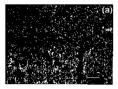
Figure lA is a scanned image of an SEM micrograph showing the
alignment of carbon nanotubes on polycrystalline nickel grown under the
conditions described in Table I (A). As observed, the carbon nanotubes are
oriented perpendicular to the substrate surface and are quite uniform in
height.
The carbon nanotubes do not grow well along the Ni grain boundaries, shown by
the two empty tracks running from upper left and from upper right down to
bottom. This is probably due to the fact that grain boundaries do not have
enough
available nickel as a catalyst. Figure 1 B is a higher magnification image of
an
area within a single nickel grain. Here, nanotube distribution uniformity
within
this grain is reasonably good. Although there is a wide distribution of carbon
nanotube diameters ranging from 60 - 500 nm, the uniformity in both diameter
and site distributions can be controlled via the growth conditions. Here,
carbon
nanotube density is about 106 nanotubes/mm2.
Figure 2 is a scanned image of an SEM micrograph showing
carbon nanotubes grown on polycrystalline nickel at a higher plasma intensity
under the conditions listed in Table 1 (B). Most of the nanotube diameters are
smaller (~ 250 nm), and their distribution is narrower, ranging from 200 to
300
nm. With increased plasma intensity, the density increased to 4 x 10⁶
nanotube/mm2, about 4 times higher than that shown in Figure 1. The increase
of
-- CA 02335449 2000-12-18
-25-
plasma intensity apparently reduces the catalytic nickel particle size, which
leads
to both thinner carbon nanotubes and improved nanotube uniformity.
Figure 3 is a scanned image of an SEM micrograph showing
carbon nanotubes grown under the conditions listed in Table 1 (C). These
carbon
~ nanotubes were synthesized at a higher plasma intensity than that used for
the
carbon nanotubes of Figure 2. In order to keep the substrates at low
temperature,
the filament current was reduced from 9 to 6 amperes. As shown in Figure 3.
the
carbon nanotubes are at least 10 ~m long, and the diameters are < 100 nm. By
increasing plasma intensity, two structural changes are readily observed.
First,
10 there is a substantial decrease in the average tube diameters from ~ 250
nm, as
shown in Figure 2, to ~ 100 nm, as shown in Figure 3. Second, the tube lengths
increase dramatically. This high growth rate is very attractive for the
potential
large-scale production of carbon nanotubes with long lengths. However, when
the diameters are < 20 nm, the tubes are less straight than for those with
diameters
1> >SOnm.
High resolution transmission electron microscopy (TEM) analysis
of the carbon nanotubes shows these film structures to be truly carbon
nanotubes,
as opposed to carbon fiber-like structures. Samples with carbon nanotubes
grown
to several microns in length were scraped off a nickel substrate directly onto
a
20 copper TEM grid for analysis. Figure 4 shows a typical image obtained for
these
carbon nanotubes. The disorder is due entirely to the random process of
nanotube
collection on the TEM grid. The dark spot at the end of each structure is a
cap of
a small ball of catalyst layer material, nickel in the instant example. This
image is
typical to those reported elsewhere demonstrating a carbon nanotube structure.
2~ Nevertheless, the insert to Figure 4, a high-resolution image of a portion
of a
typical carbon nanotube structure, is more convincing. The width of this tube
is
30 nm and represents a highly defected mufti-walled structure with a hollow
core.
The core diameter is about 20 nm and the wall thickness is about 5-10 nm. The
fringes on each side of the tube identify individual cylindrical graphitic
layers.
30 This particular carbon nanotube is a structure with approximately 15 walls
of
graphitized carbon. Both the angular bend in the structure and the appearance
of
carbon walls running across the diameter of the nanotube demonstrate
structural
defects suggestive of twisting of the nanotube structure. As can be seen at
the
CA 02335449 2000-12-18
-26-
structural defects, non-continuous walls intersect one another. On an atomic
scale, the defects create active surface cites for permeability through the
nanotube
structure. The lack of fringes inside the nanotube, as well as the lighter
contrast as
compared to the nanotube walls, indicates that the core of the structure is
hollow.
Example 2
Substrate Preparation
Display glass having a strain point temperature of 666°C was cut
into 10 x 5 mm pieces and cleaned in acetone by ultra-sonication. The cleaned
pieces were mounted onto the surface of a stainless steel resistive heater,
and the
10 whole assembly was placed into a magnetron sputtering chamber. The chamber
was pumped down below 8 x 10'6 Ton before argon gas was introduced into the
chamber to maintain a working pressure of 20-60 mTorr. A nickel catalyst layer
of 15 to 60 nm in thickness was deposited onto the glass substrates by
magnetron
sputtering for about 1.5 to 6 minutes. During deposition, the substrates were
15 either heated or kept at room temperature.
Catalyst layered substrates were placed to a CVD chamber, which
was pumped down below 6 x 10'6 Torr. As, soon as the chamber pressure reached
6 x 10'6 Torr, acetylene and ammonia gases were introduced into the chamber to
maintain a working pressure of 1 - 20 Torr during carbon nanotube growth. The
20 total flow rate of acetylene and ammonia gases was 120 - 200 sccm with a
volume ratio of acetylene to ammonia varying from 1: 2 to 1:10. After the
working pressure stabilized, the power to the tungsten filament coil and to
the
plasma-generator, as described in Example 1, were energized to generate heat
and
plasma at a temperature below 666°C to induce carbon nanotube growth
under the
25 conditions listed in Table 2. Carbon nanotube samples were examined in the
manner described in Example 1. In particular, scanning electron microscopy was
used to investigate the effect of various growth conditions on the morphology
of
carbon nanotubes grown on nickel-coated display glass.
As described in Table 2(A), NH3 was introduced during the first 5
30 minutes without introducing C2H2. During this time, the catalyst layer was
plasma
etched to reduce its thickness to less than 40 nm. After these initial 5
minutes,
CZHZ was introduced. Immediately, a color change occurred as a result of the
growth of carbon nanotubes. The growth period lasted only 10 minutes.
CA 02335449 2000-12-18
_27_
Referring to Figures SA-B, in order to examine the orientation and alignment
of
the carbon nanotubes on the glass substrates, part of the carbon nanotube-
covered
area was peeled off (lower left in Figure SA) with a tweezer to expose the
glass
substrate. During peeling, another area was crumpled (lower right in Figure
SA),
~ and a long scratch was made on the peeled open area (lower left in Figure
SA).
Under visual and SEM observations, the alignment of the carbon nanotubes
across
the whole surface w°as as uniform as in the upper part of Figure SA. To
estimate
the carbon nanotube length, an SEM was taken at higher magnification along the
peeled edge (Figure 5B). Misalignment of the carbon nanotubes on the peeled
I 0 edge resulted from the peeling operation. From Figure SB, it was estimated
that
the nanotubes were about 100 nm in diameter and 20 ~m in length. Given the
growth time of 10 minutes, the growth rate was calculated to be 120 ~m / hour,
about 5 times faster than the value reported in Li.
As respectively shown in Figures 6A and 6B, the surfaces of the
1 ~ nickel layer after the initial NH3 or N2 plasma etching are essentially
the same.
The plasma etching conditions are respectively listed in Table 2(B) and 2(C).
For
comparison, Figure 6C shows the as-sputtered smooth nickel surface. Although
both NH3 and N2 plasma etching roughen the nickel surface, the roughing of the
nickel surface is not responsible for the nucleation and growth of carbon
20 nanotubes.
Interestingly, when the sequence of gas introduction is reversed,
that is, when CZH~ is introduced first, 5 minutes later, followed by NH3, no
growth
of carbon nanotubes is observed, only amorphous carbon is formed on the nickel
surface. The amorphous carbon layer forms in the first 5 minutes and CZHZ
25 plasma covered the nickel surface to inhibit the catalytic role of nickel
so that
there is no growth of carbon nanotubes. Apparently, carbon nanotubes grow only
when catalyst gas (NH3) is introduced first followed by the carbon source gas
(CzH2) or both the carbon source and catalyst gases (CZHZ and NH3,
respectively)
are introduced simultaneously. Thus, it may be concluded that NH3 plays a
30 crucial catalytic role together with the nickel layer to promote the growth
of the
carbon nanotubes. The catalytic role of NH3 is further confirmed by the fact
that
there is no carbon nanotube growth when NH3 was replaced by N2 gas at
temperatures below 700°C with other conditions unchanged. However,
carbon
- CA 02335449 2000-12-18
-28-
nanotubes do grow when NH3 is replaced by NZ at temperatures above
700°C
utilizing PE-HF-CVD.
In order to examine the effect of thickness of the metal catalyst
layer on the growth of carbon nanotubes, CzHz and NH3 were introduced at the
5 same time under the conditions listed in Table 2(D). Under these growth
conditions, no plasma etching occurred, and the nickel layer remained 40 nm
thick.
Referring to Figure 7A, carbon nanotubes have an estimated site
density of about 10' tubes/mm2. The diameters of the carbon nanotubes (Figure
10 7A) are much larger than those in Figure SB. From Figure 7B, it is
estimated that
the outside diameters of the carbon nanotubes range from 180 to 350 nm, and
most of the carbon nanotubes are about 250 nm in diameter. Although not shown,
carbon nanotubes have been grown in accordance with this method with diameters
as large as 500 nm. This experiment clearly shows that as the catalyst layer
15 thickness is reduced, the diameters of the resultingly grown carbon
nanotubes are
likewise reduced. As shown in Figure 7B, the catalytic role of nickel is also
clearly indicated by the nickel cap on the tip of each nanotube.
Interestingly, one
carbon nanotube, as indicated by an arrow in Figure 7B, does not have a nickel
cap. Due to the absence of a cap on the identified nanotube, it may be
concluded
20 that the carbon nanotubes are empty with a very thin wall. In support of
this
conclusion, another carbon nanotube is viewable behind the capless one through
its wall. Surprisingly, the nanotubes have a central core which is larger than
reported values in literature. These large carbon nanotubes may be useful for
applications such as storage of gases, such as HZ, and as microelectrodes.
25 These experiments show a direct relationship between metal
catalyst layer thickness and nanotube diameters. That is, the thinner the
nickel
layer, the thinner the nanotubes. To examine further the effect of nickel
layer
thickness on carbon nanotube growth, a much thinner nickel layer of only 15 nm
is utilized under the conditions listed in Table 2(E) and 2(F). In one
experiment
30 (Table 2(F)), the nickel layer thickness is plasma etching reduced by
introducing
NH3 first, and 20 minutes later introducing CZHZ. In Figures 8A and 8B,
respectively, SEM micrographs of carbon nanotubes grown under the conditions
listed in Table 2(E) and 2(F) show the dependent relationship of nanotube
- CA 02335449 2000-12-18
-29-
diameter to the nickel layer thickness. The typical diameter of the nanotubes
in
Figure 8A is only about 65 nm, compared to 240 nm in Figure 7B. Relatively
speaking, the alignment in Figure 8A is not quite as good as in Figure 7B. A
comparison of Figures 8A and 8B demonstrates that 20 minutes of plasma etching
reduces the thickness of nickel layer, which in turn results in even thinner
carbon
nanotubes with typical diameters of only about 20 nm. The comparison also
shows that the alignment begins to deviate when the nanotube diameter is
reduced
to 20 nm. Carbon nanotubes have been produced in accordance with this method
having a diameter as small as 4 nm. Therefore, for applications requiring
10 substantial nanotube alignment, it is apparent that diameters should be
larger than
50 nm for carbon nanotubes having a length of 20 p,m or longer.
Again. high-resolution TEM was utilized to determine the interior
and wall structures of the carbon nanotubes. Samples for a plan view TEM were
prepared as follows. Given the flexible nature of the nanotubes, the carbon
1 ~ nanotube film was penetrated with M-Bond 610 epoxy resin (M-Line
Accessories)
to provide mechanical stiffness. This resin has very low viscosity and curing
is
time/temperature dependent. Hydrotetrafuran (diethylene oxide) makes up about
90% of the composition of M-Bond. The carbon nanotube film was immersed in
acetone; then M-Bond epoxy is slowly added until a l :l ratio is attained. The
20 sample was cured at room temperature for 48 hours. Because the viscosity of
the
epoxy was very low when introduced to the sample, it easily impregnated the
pores to completely mix with the acetone. Standard mechanical thinning and ion
milling (low angle, low voltage and current) was used to thin the sample to
electron transparency. Most of the substrate was removed mechanically,
followed
'_'~ by ion milling until the film was exposed. Then, both sides were ion
milled for 15
minutes.
Figure 9A shows a cross-sectional view of a typical thinner carbon
nanotube. This carbon nanotube is a mufti-walled central hollow tube with an
outside diameter of nearly 30 nm. The fringes on each side of the tube
represent
30 individual cylindrical graphitic layers. This particular carbon nanotube
has
approximately 15 walls of graphitized carbon. Both the angular bend in the
structure and the appearance of carbon walls running across the diameter of
the
nanotube demonstrate structural defects suggestive of twisting of the nanotube
CA 02335449 2000-12-18
-30-
structure. The lack of fringes inside the tube, as well as the lighter
contrast
compared to the nanotube walls indicates that the core of the structure is
hollow.
Further evidence of the hollow core is shown in Figure 9B. This is
a high-resolution plan view TEM image of a single carbon nanotube structure.
5 Here, the hollow nature of the nanotube, again represented by the lighter
contrast
of the inner core, is more readily observable. The disorder seen in the wall
fringes
circumventing the hollow center are most likely caused by the twist-like
defects
throughout the carbon nanotube length as shown in Figure 9A. These high-
resolution TEM images show that the structures are hollow, mufti-walled carbon
10 nanotubes with defects existing along the tube. The defects of bending and
twisting of the carbon nanotubes of the thin carbon nanotubes shown in Figures
9A and 9B are consistent with the SEM observation in Figure 8B. Further, there
is a inverse relationship between CVD temperature and defect density. As the
deposition temperature is reduced, the carbon nanotubes demonstrate an
increase
15 in the number of defects which occur in the wall. On an atomic scale, these
defects render the wall of the carbon nanotube discontinuous. This results in
an
extremely high, active, and accessible surface area due to the substantial
alignment of and relatively large spacing between the carbon nanotubes. These
discontinuations in the wall structure provide atomic disorder which results
in an
20 active surface through which atomic level diffusion can occur.
Table 2. Growth conditions for nanotubes shown in Figures 5, 6, 7, and 8.
C~HZ / NH3 / N~ Filament Current Plasma Intensity Growth Time
25 (sccm / sccm) (amperage, A) (amperage / voltage / (minutes)
watts)
(A): For Figures SA and 5B:
0 /160/0 8.5 0.10/635/72 5
30 followed by
80/160/0 8.5 0.13/670/95 10
(B): For Figure 6A:
0/ 160/0 8.5 0.09/740/66 3
35
(C): For Figure 6B:
0/0/296 8.5 0.10/480/53 3
CA 02335449 2000-12-18
-31-
(D): For Figures 7A and 7B:
80 / 160 / 0 8.5 0.20 / 700 / 150 25
5 (E): For Figure 8A:
40/ 160/0 7.2 0.13/650/90 14
(Fj: For Figure 8B:
0/ 160/0 8.0 0.10/480/52 20
10 followed by
80/ 160/0 8.2 0.10/560/60 10
Example 3
15 A glass substrate was prepared as in Example 2 with a 10-40 nm
thick nickel catalyst layer having an as-sputtered smooth surface, as shown in
Figure 6C. Carbon nanotubes were grown by PE-HF-CVD for about 10 minutes
as in Examples 1 and 2, except the acetylene and ammonia volume ratio was 1:2
to 1:4. Figure 10 shows a large area growth of substantially vertically
aligned
20 carbon nanotubes. The length of the carbon nanotubes is up to 50 Vim. The
diameters are estimated to be in the range of 100 - 150 nm (See Figure 14).
Example 4
Single crystal, p-type boron doped 9.5 S2-cm (100) silicon
substrates were prepared as in Example 2 with a 10-40 nm thick nickel catalyst
25 layer having an as-sputtered smooth surface, as shown in Figure 6C. Carbon
nanotubes were grown by PE-HF-CVD as in Examples 1 and 2, except the
acetylene to ammonia volume ratio was 1:2 to 1:4. Figures 11 and 12 show
carbon nanotubes which were grown for 5 and 2 minutes, respectively. Referring
to Figure 11, substantially perpendicular carbon nanotube alignment is clearly
30 shown. A nickel cap. which acts as a catalyst to sustain growth, is also
discernible
at the top of each carbon nanotube. Early stage carbon nanotube growth is
shown
Figure 12, since the growth was stopped at 2 minutes. The shortest nanotubes
are
about 0.1 pm.
Example 5
35 Carbon nanotubes were grown as in Example 3. The catalyst metal
caps were thereafter removed by HNO; solution etching and Ar ion sputtering.
CA 02335449 2000-12-18
-32-
Figures 13 and 14 show the SEM image of the nanotubes after removal of the
nickel caps by HNO; solution etching and Ar ion sputtering, respectively. The
solution etching by HN03 only took about one minute, and the removal of nickel
caps is complete. As shown in Figure 13, the ends of the carbon nanotubes are
5 open after etching. Morphologically, there was no observable damage by the
HN03 etching. In Figure 14, all the nanotubes were bent by the Ar ion
sputtering,
and the nickel caps were not completely removed. These techniques may be
utilized to remove any of the metal or metal alloy caps. By removing the caps,
various fillings (i.e. hydrogen, lithium ions, bismuth, lead telluride,
bismuth
10 tritelluride, a pharmacological agent, etc.) can be added to the nanotube
core.
Thereafter, if desired, the open ends can be sealed by electrochemical
deposition
of a metal onto the carbon nanotubes.
Example 6
Carbon nanotubes were grown as in Example 3, except the
15 substrates were placed in the CVD chamber at differing angles with respect
to the
plasma generator. Although the carbon nanotubes grew substantially aligned
with
one another, the alignment was independent of substrate surface topography.
Figures 15 and 16 show the SEM image taken from side and top on a sample sit
tilted at a certain angle during growth. It is observed that carbon nanotube
20 alignment is not perpendicular to the substrate surface, but rather is
angled with
respect to the substrate. The tilt direction is closely related to the
direction of the
electrical field which generates the plasma. This technique may be utilized to
grow aligned carbon nanotubes at any angle with respect to the substrate,
including nanotubes lying in a plane.
25 Example 7
A catalyst layer of nickel was deposited on a p-type boron doped
9.5 S2-cm (100) silicon substrate by electron beam lithography and metal
evaporation. A bilayer electron-beam resist (5% 100 molecular weight
polymethylmethacralate) was capped by 2% 950 molecular weight
30 polymethylmethacralate that was patterned with a JEOL J6400 SEM converted
for
lithography. The resist was developed in a solution of methyl isobutyl ketone
and
isopropyl alcohol (3:1 ). Thereafter, 150 of nickel was deposited by electron
CA 02335449 2000-12-18
-33-
beam evaporation. A catalyst layer (i.e. a large, ~ 0.25 mm2 nickel pad or one
or
more nano-dots) remained after resist/metal liftoff in acetone.
Carbon nanotubes were grown by PE-HF-CVD as in the process in
Example 2, except growth was performed at a pressure of 1-10 Torr with an
5 acetylene to ammonia volume mixture of 1:4 at a total flow rate of 200 scan
for
about 5 minutes.
Referring to Figures 17A-B, scanned images of SEM micrographs
show carbon nanotubes grown on the silicon substrate in the region of the edge
of
the nickel pad. As shown in Figure 17A, absence of nanotube growth in the
10 foreground demonstrates selective growth on the nickel catalyst film and
not on
the silicon substrate. Figure 17B shows these nanotubes after being
mechanically
broken using tweezers. Surprisingly, the tubes break somewhere along the tube
and not at the interface between the nickel and silicon. This observation is
different that that of nickel-on-glass nanotube growth, where the nanotubes
broke
15 cleanly at the nickel-glass interface, as shown in Figure SA.
Example 8
Nickel catalyst nano-dot patterns were deposited on a p-type boron
doped 9.5 S2-cm ( 100) silicon substrate by electron beam lithography and
metal
evaporation as in Example 7. Carbon nanotubes were grown by PE-HF-CVD as
20 in the process in Example 7, except the growth temperature was between
300°C
and 666°C and only a single, free-standing carbon nanotube grew on each
nickel
nano-dot. Thereafter, carbon samples were examined by SEM, TEM, XPS, etc.
techniques as discussed above.
Figure 18 is a series of SEM micrographs illustrating the growth of
25 single, multiwall carbon nanotube obelisks on respective nickel catalyst
nano-
dots. The catalyst nano-dots are shown in arrays of 100 nm catalyst nano-dots.
The site and spacing are precisely controlled. Figures 18A, 18C, 18E, and 18F
are
perspective views of the nanotubes, and Figures 18B and 18D are top views of
the
nanotubes. Figures 18A and 18B demonstrate selective growth of the nanotubes
30 on the several repeated array patterns. The nanotubes accurately reflect
the
spacing and periodicity of the lithographically patterned catalyst nano-dots.
Figures 18C and 18D reflect higher magnification and show the repeated array
CA 02335449 2000-12-18
-34-
pattern where the nanotubes are spaced either 2 ~m apart (left portion of
array) or
1 ~m apart (right portion of array).
The sharp, tapered tips of the nanotubes shown in Figures 18E,
18F, and 19 are unique to carbon nanotubes grown on nano-dots under the
instant
conditions. Notable, such nanotubes do not have a cap of the catalyst
material. In
Figure 18F, the nano-dots are spaced 5 ~m apart. The non-uniformity of height
(0.1 to ~ Vim) is apparently not related to the spatial position. Rather, it
is believed
to be due to non-uniform electron beam lithography and electron beam
evaporation of the catalyst nano-dots onto the substrate. With precise control
of
the electron beam lithography, all carbon nanotubes should be substantially
uniform in height. Nanotube length is dependent upon the growth time and the
thickness of the nano-dot, whereas nanotube diameter depends upon the diameter
of the nano-dot. It can be observed that although the heights vary, the
diameters
are generally uniform at 150 nm. By utilizing controlled nano-dot placement on
1 ~ the substrate, single or multiple carbon nanotubes with controlled site
density can
be achieved. For example, the direct growth of a single carbon nanotube on the
probe tip of scanning tunneling microscope~(STM), atomic force microscope
(AFM), etc. may be achieved. Well-defined spacing of multiple carbon nanotubes
with mufti-electron beam lithography can improve the patterning ability by 104
-
106 times.
Although the invention has been described in detail for the purpose
of illustration, it is understood that such detail is solely for that purpose,
and
variations can be made therein by those skilled in the art without departing
from
the spirit and scope of the invention which is defined by the following
claims.