Note: Descriptions are shown in the official language in which they were submitted.
CA 02335480 2000-12-19
WO 00/00818 PCT/US99/14436
OPTOELECTRONfC APPARATUS
FOR DETECTING DAMAGED GRAIN
Technical Field
The invention is directed to a novel short-wave U.V. excited, (herein, short-
wave U.V.
is defined as U.V. light having a wavelength of 300 nm or less) fluorescence
sensor used to
detect levels of damage in grains or seeds, including but not limited to
cracked or broken
conditions in the grain or biological contamination. This sensor can be used
on grain that is in
either a stationary or a moving state, and therefore can be used in an
operating combine
harvester (hereinafter combine), in a grain elevator for quality ooMrol, or as
a hand held
detecting device. Hereinafter, the sensor will be referred to as either a
cracked grain sensor
or simply a sensor.
ground Art
The prior art suggests the desirability of having an effective method for
detecting grain
which has been mechanically damaged, or cxacked. Mary of the methods which
have been
hitherto developed are only usable in a laboratory setting, and are not
adaptable to real-time
use in a combine or in milling and grain handling operations.
Some methods require that a chemical solution be applied to the grain (U.S.
Patent
Nos. 4,000,875 and 4,020,882}, which can render such grain harmful for human
or animal
consumption. Other methods require undue destructive sample preparation (U.S.
Patent No.
4,000,975), which precludes the use of those methods for real-time detection
of damaged
grain kernels in a continuous flo\nr of grain material.
U.S. Patent No. 4,572,666 discloses a through-beam method for the detection of
cracked rice, in which a coherent light beam is passed through individual rice
grains. Such a
method is limited to grain of a translucent nature and can only be used with
small quantities of
grain, such as in a laboratory setting.
U.S. Patent No. 4,348,855 proposes an arrangement of sieves and impact
transducers
(similar to those used for grain loss monitoring) to separate and detect
damaged grain inside a
combine. However, this method does not adequately discriminate between small
but intact
grain kernels versus pieces of debris and broken pieces of larger grain
kernels.
Infran~d and near-infrared methods such as described in U.S. PateM Nos.
5,132,538,
4,806,764, and 5,751,421 are used primarily to determine the constituents of
grain, such as
oil, protein, starch, and moisture and are not intended for damage detection.
Likewise, U.S.
Patent No. 4,421,772, which uses a range of visible, ultraviolet and/or X ray
radiation to
determine characteristic fluorescence from the component parts of ground seeds
and other
botanical master, is not targeted for grain damage detection. However, this
patent teaches the
CA 02335480 2000-12-19
WO 00/00818 PCT/US99/14436
use of short-wave UV as an optimum excitation wavelength for the detection of
fluorescence
emission related to the starchy endosperm of grains.
Other methods use either machine vision under visible light (see "Image
Processing
and Neural Networks Classify Complex Defects" by ~Ison, in Vision Systems
Desi4n, March,
1999) or machine vision augmented with long-wave UV light (U.S. Patent Number
4,713,781)
Machine vision requires expensive imaging components, such as CCD cameras,
artificial
illumination, and complex signal processing means. Despite progress in the
pertom~ance of
machine vision systems, the complexity of the task does not allow for
processing speeds
essential to real-time applications. Also, the use of a CCD camera dictates
the selection of
long-wave UV excitation, rather than the more effective short-wave UV
excitation, thereby
impairing the capability of accurately determining the presence of damaged
grain, because
more background light from the source reaches the detector.
Disclosure of the Invention
A first object of the present invention is to provide an apparatus for
detecting levels of
damage in grains or seeds, including but not limited to cracked or broken
conditions in the
grain. A second object of the present invention is to provide a short-wave
U.V. excited
fluorescence sensor which will detect levels of damage in grains or seeds in a
fast, accurate,
and consistent manner. A third object of the present invention is to provide a
damaged grain
sensor applicable to grain that is in either a stationary or a moving state,
and therefore the
sensor can be used in an operating combine, in a grain elevator for quality
control, or as a
hand held detecting device.
These and other objectives are achieved by the present invention, which
includes an
ultraviolet light source that provides a certain short-wave UV excitation
wavelength (e.g.,
253.8 nm) to which the grain is exposed. Different constituents of grain emit
different levels of
fluorescence. The endosperm of grain, when exposed to said certain excitation
wavelength
will fluoresce at a certain emission wavelength (e.g., 335 nm) with a
substantially higher
intensity than will the pericarp, or hull of the grain. Therefore, if grain
has been damaged,
such that the grain has been cracked or broken so as to expose the endosperm,
a
measurable difference in fluorescence intensity can be detected between the
damaged and
undamaged states of the grain by using a non-imaging photon detector. Other
elements of
the invention are present in order to concentrate the desired fluorescence
signal on the non-
imaging photon detector and to process the signal from the photon detector.
The present invention is advantageous as compared to the prior art in that the
sample
is not exposed to chemicals. Nor is undue preparation of the sample or
destruction of the
sample required. The present invention can be used with a wide variety of
grain types and is
not reliant upon through-beam illumination, which is unsuitable for high
volume flow as well as
2
CA 02335480 2000-12-19
WO 00/00818 PCT/US99/14436
for measuring damage to grains that are not translucent. Because the present
invention does
not rely on imaging of the sample onto the detector, optical components that
may be used
to gather light in order to concentrate the luminescence onto the detector can
be inexpensive.
Further, the complexity of signal processing is drastically reduced and the
signal processing
time is shortened so that real-time measurement applications are feasible.
Additionally, the
present invention allows the use of more effective, short-wave UV radiation
for fluorescence
excitation, which minimizes the detection of false signals. For the above
reasons the
apparatus of the present invention may be built of standard electronic and
optical components
that are avai~ble at low cost.
Brief Description of the Drawings
The present invention will become more fully understood from the detailed
description
given below and the accompanying drawings, which are given by way of
illustration only and
thus are not limitative of the present invention, wherein:
Fig. 1 shows the component configuration of a first embodiment of the sensor
of the
present invention,
Fig. 2 illustrates the excitation light as it is separated into two wavelength
components
by a dichroic beam-splitter,
Fig. 3 illustrates the combined fluorescence emission and scattered/reflected
excitation
light as it is separated into two wavelength components by the dichroic beam-
spfitter,
Fig. 4 shows the component configuration of a second embodiment of the sensor
of
the present invention, wherein there is provided an alternative sensor window
configuration,
and
Fig. 5 sh~us the areas on a combine which have been identified for possible
placement of the cracked grain sensor.
Best Mode for Carrvin~i Out the Invention
The following description of the preferred embodiments directed to a damaged
grain
sensor is merely exemplary in nature and is in no way intended to limit the
invention or its
applications or uses. For simplification, discussion of the damaged grain will
be directed to
cracked or broken grain within a combine. The data obtained from the damaged
grain
sensors) can be displayed to the combine operator, who can adjust grain
separation and
grain cleaning devices in a manner so that a predefined level of grain quality
is maintained.
Aftematively, the data from the damaged grain sensors) can be fed into a
closed loop control
system to allow automatic adjustment of the combine settings.
It has been established that, when exposed to a certain UV excitation
wavelength
(e.g., 253.6 nm), different constituents of grain emit different levels of
fluorescence. The
endosperm of grain, when exposed to this excitation wavelength, will fluoresce
at a certain
3
CA 02335480 2000-12-19
WO 00/00818 PCTNS99/14436
emission wavelength (e.g., 335 nm) with a substantially higher intensity than
will the pericarp,
or hull of the grain. Therefore, if grain has been damaged to the extent of
being cracked or
broken so as to expose the endosperm, a measurable difference in fluorescence
intensity can
be detected between the damaged and undamaged states of the grain.
It is to be understood that parts of the grain other than the endosperm can be
targeted
{e.g., the aieurone), by using different excitation wavelengths and monitoring
different
emission wavelengths, thereby targeting a different part of the damaged grain
kernel.
Fig. 1 is a diagram illustrating an embodiment of the component configuration
of the
sensor. The embodiment of the invention depicted in Fig. 1 is configured to be
used as a
cracked or broken grain sensor in an operating combine, in a grain elevator
for quality control,
or as a hand held detecting device. In the application as a sensor for
detecting cracked or
broken grain, a certain UV excitation wavelength is emitted (e.g., 253.6 nm)
and a certain UV
emission wavelength is monitored (e.g., 335 nm).
It is to be understood that other embodiments of the invention (not
illustrated) may
target (i.e., include) the detection of other types of grain damage, such as
biological
contamination (e.g., mold, mildew, or insects), and can require the use of one
or more
different UV excitation wavelengths and the monitoring of one or more
different UV emission
wavelengths. Embodiments for such applications may require other
configurations, which
would include multiple components of differing parameters (e.g., two or more
detectors for
different wavelengths). Also, the collection of additional photonic
information (e.g., detection
of reflected light for mass flow extrapolation) may require the addition of
components that
might require a change in the sensor configuration.
Information from other existing sensors that are part of a modem combine
(e.g., clean
grain yield or mass flow sensor, tailings sensor, grain moisture sensor) can
also be used in
conjunction with the damaged grain sensor. This is commonly referred to as a
fused sensor
concept and can further enhance the usefulness of the damaged grain sensor.
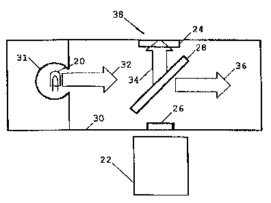
A light source 20, preferably consisting of an uncoated knhr pressure UV
mercury lamp,
supplies the excitation wavelengths) for the sensor. A photon detector 22,
which can be a
photo multiplier tube (PMT) or a silicon detector especially designed for the
detection of short-
wave UV (e.g., Siemens ultraviolet selective sensor SFH 530), is used as the
sensor detector.
A sensor window 24 is provided adjacent a measurement region 38 to separate
the
optoelectronic components of the sensor from grain (not illustrated) located
at the
measurement region. The sensor window 24 is preferably made of sapphire
because of its
ability to pass UV radiation and its durability and scratch resistance. In
certain applications
(e.g., hand held devices) where abrasion is not a concern, less expensive
quartz may be used
for the sensor window 24. On a combine, however, the abrasion caused by debris
and sand
4
CA 02335480 2000-12-19
WO 00/00818 ~ PCTNS99/14436
moving rapidly across the window would quickly frost up quartz and, therefore,
sapphire is
recommended for such an operating environment.
A filter 28 may be provided as a wavelength selector. In one embodiment the
filter 26
is a bandpass filter centered at 335 nm with a bandpass of 20 nm (335 nm
coincides with the
wavelength of ma~amum intensity of the fluorescence for endosperm of grain
excited with light
at 253.8 nm wavelength). An inherent disadvantage of such a f~ter is that the
transmission
efficiency even at its nominal pass wavelength is typically only 30 percent.
Thus, most of the
fluorescence that is generated by the grain is lost. In other embodiments, the
filter 26 can be
changed to accept different wavelength ranges.
A sensor sensitive in different wavelength ranges could be substituted in
order to
enhance the photon detecting capability for solid state photon detection or to
target the UV
sensor for the detecti~ of speafic grain damage, such as the presence of
biological
contaminants or cracks in the grain kernel. Two reasons to vary the parameters
of the filter 26
would be: to increase the fluorescence signal throughput, so that a solid
state photon detector
can be used; and to enable an estimate of the actual mass flow of grain
passing by the sensor
window 24 by monitoring sensor signal fluctuations due to the fluorescence of
the pericarp of
the grain. Mass flow estimates can also be obtained from another sensor within
the combine,
e.g., a clean grain yield sensor (not shown). in some embodiments (not
illustrated), filter 26
may be eliminated, due to the wavelength selective capabilities of the
dichroic beam spiitter 28
and the fact that certain photon detectors 22 having filters that are formed
integrally with the
photon detector.
In the preferred embodiment, a dichroic beam-splitter 28 is used as the
wavelength
selector to isolate the excitation wavelength (e.g., 253.8 nm) emitted by the
light source 20
from as much of the longer fluorescence output wavelengths as possible. The
dichroic beam-
splitter 28, in this embodiment, is a 288 nm long-pass filter. Substantially
all the light from the
light source 20 of a wavelength shorter than 288 nm is reflected toward the
sensor window 24.
The light having wavelengths that are longer than approximately 300 nm is
transmitted with
about 85-90 percent effiaency through the beam-splatter and into a beam dump
30.
The dichroic beam-splatter 28 also filters UV radiation emitted from the
exposed
endosperm of the grain that is present at the measurement region 38 on the
outer side of the
sensor window 24. The dichroic beam-spiitter 28 filters in such a way that
light emissions and
scatteredlreflected light shorter than 288 nm are reflected and any light
emissions and
scattered light longer in wavelength than approximately 300 nm are allowed to
pass through.
The light emissions of interest from the endosperm are of wavelengths longer
than 300 nm, so
it passes through the dichroic beam-spiitter 28 to the bandpass filter 26 and
to the photon
5
CA 02335480 2000-12-19
WO 00/00818 PCT/US99/14436
detector 22. In the described embodiment, the dichroic beam-splitter 28 is
manufactured to
operate at a 45 degree angle with respect to the incident radiation.
The entire interior, excluding the light source cavity 31, is covered with a
light
absorbing material, such as black paint or other surface treatment, and acts
as a beam dump
30 to absorb unwanted light.
Fig. 2 illustrates the excitation light as it is separated into two wavelength
components
by a dichroic beam-splitter. Light 32 from the light source 20 is incident on
the dichroic beam-
splitter 28 at a substantially 45 degree angle, with respect to the plane of
the filter 26. Light
32 from the light source 20 includes all wavelengths output by the light
source 20. Light 32 is
incident on the dichroic beam-splitter 28 and is separated into a short
wavelength constituent
34 and a long wavelength constituent 36. The short wavelength constituent 34
includes the
predominant 254 nm emission line radiation from the light source 20 and is
reflected toward
the sensor window 24. The long wavelength constituent 36, in this embodiment,
includes all
radiation greater than approximately 300 nm, which is transmitted through the
dichroic beam
splitter 28 and is absorbed in the beam dump 30.
Fig. 3 illustrates the fluorescence and scattered/reflected excitation light
as it is
separated into two wavelength components by the dichroic beam-splitter 28.
Light 40, which
passes through the sensor window 24, consists of scattered light from the
light source 20,
including reflected light from short wavelength constituent 34 (Fig. 2), and
fluorescent light
emitted from grain kx~ted at measurement region 38. The light 40 is incident
on the dichroic
beam splitter 28 and is separated into a short wavelength constituent 42 and a
long
wavelength constituent 44. Short wavelength constituent 42 consists of
wavelengths of 288
nm and shorter, including the 253.6 nm wavelength radiated from the light
source 20. The
short wavelength constituent 42 is reflected from the mirrored surface of the
dichroic beam
splitter 28 and is absorbed in the beam dump 30. The long wavelength
constituent 44
consists of wavelengths of 300 nm and longer, including the fluorescence
emission
wavelengths (i.e., near 335 nm) from grain located at measurement region 38.
This long
wavelength constituent is then incident on the filter 28.
Fig. 4 is a diagram which shows the component configuration of a second
embodiment
of the apparatus of the present invention, wherein there is provided an
aitemative sensor
window configuration. In the previous embodiments, the sensor window 24 is
parallel to the
filter 26 surface. In order to reduce the back-scatter from the light source
20, an embodiment
in which the sensor window 24 is angled and physically reflects the back-
scatter away from
the photon detector 22 is devised. The embodiment illustrated in Fig. 4
depicts the sensor
window 24 tilted at a small angle (e:g., 5 - 10 degrees) with respect to the
plane defined by the
6
CA 02335480 2006-03-03
filter 26, and in a direction such that the angle between the surface of the
dichroic beam-
splitter 28 and the surtace of the window 24 is greater than 45 degrees.
In another embodiment (not shown), the sensor window 24 of the sensor is
tilted at
an angle of 5 - 45 degrees with respect to the plane defined by the filter 26,
and in a direction
such that the angle between the surface of the dichroic beam-splitter 28 and
the surface of
the window 24 is less than 45 degrees.
Fig. 5 is a drawing of a combine an which areas have been identified for
possible
placement of the cracked grain sensor. These areas include, but are not
limited to, the grain
conveyance area 50 that is located directly under the concave 48, the
chafferlsieve area 52,
~o the exit from the cleaning shoe 54, and the dean grain elevator 56. Placing
the sensor in the
grain shuttle area 50 will yield information on the actual amount of cracked
grain that is being
generated in the threshing process. This infomtation can be used to indicate
changes in the
threshing effidency during harvest, if used as a relative measurement. In
conjunction with
mass flow or yield measurements, information from the grain shuttle area 50
will indicate the
15 actual percentage of grain being damaged in the threshing process. Data
gathered from the
chaffer/sieve area 52 indicates how much of the grain being cxadked is small
enough to be
excluded from the clean grain system. If placed at the exit of the cleaning
shoe 54, the data
will indicate the relative amount of cracked grain that is being expelled from
the combine.
Data gathered from the dean grain system 56 will yield information on the
percentage of
2o cracked grain that will be delivered to the market. The aadked grain sensor
can also be
placed in the grain conveyance mechanism that is underneath the threshing
mechanism or
in the dean grain elevator or in the dean grain unloading system of the
combine harvester.
Use of two or more damaged grain sensors in different places on the combine
will give a
good indication of the overall efficiency of the combining process.
25 Industrial AppG~bili
As discussed above, the invention has uses as a damaged grain sensor for grain
that
is in either a stationary or a moving state, and then:fore the sensor can be
used in an
operating combine, in a grain elevator for quality control, or as a hand held
detecting device_
The invention being thus described, it will be obvious that the same may be
varied in
3o many ways. For example, a lens or reflector may be used to concentrate the
fluorescent
radiation onto a detecting surface of the non-imaging photon detecting device.
Such lens or
reflector may be made integral with the non-imaging photon detecting device or
may be a
separate component. Such variations are not to be regarded as a departure from
the spirit
and scope of the invention. Rather, the scope of the invention shall be
defined as set forth in
35 the following claims and their legal equivalents. All such mod~cations as
would be obvious
to one skilled in the art are intended to be included within the scope of the
following claims.
7