Note: Descriptions are shown in the official language in which they were submitted.
CA 02336895 2001-11-16
DESCRIPTION
Flat Display
TECHNICAL FIELD
The present invention relates to a flat type display
device called PDP.
BACRGRC~UND ART
A conventional flat type display device called PDP
(Plasma Display Panel) having the most popular structure is so-
called double-electrode opposed discharge type PDP. In this
double-electrode opposed discharge type PDP, first and second
electrodes, each comprised of plural stripe-like electrodes
which opposes each other across a discharge space while
intersecting each other, are provided on glass substrates on
front and rear sides composing a tube containing discharge gas,
the front and rear sides being disposed in parallel to each
other. A voltage is selectively applied between plural
electrodes each composing the first and second electrodes so as
to generate discharge at an intersecting point of selected
electrodes to attain luminescent display.
Although such PDP is originally a single-color
luminescent display device, a color PDP can be constructed by
forming red, green and blue light-producing fluorescent layers
cyclically in order at predetermined positions in the tube such
that they are coated and then irradiating ultraviolet ray
generated by discharge to those fluorescent layers so as to
CA 02336895 2001-11-16
allow them to generate lights.
In such color PDP, because the fluorescent layers must
be formied at positions where scattered substances from the
electrodes and the like, generated by discharge in the tube or
ion impact cannot adhere easily, the formation positions for the
fluorescent layers are limited. Further, there is a fear that a
sufficient luminance cannot be obtained from the fluorescent
layers depending on the position in which the fluorescent layer
is formed.
The conventional color PDP involves a double-electrode
discharge type color PDP in which XY electrodes are disposed on
the same plane of the rear side glass substrate such that they
intersect each other and the fluorescent layer is formed on the
front side glass substrate.
Hereinafter, a structure of the conventional double-
electrode discharge type color PDP will be described with
reference to FIGS. 1, 2. The first electrode (X electrode) 2
comprised of plural stripe-like electrodes is disposed on the
rear side glass substrate 1 and then, the second electrode (Y
electrode) comprised of plural stripe-like electrodes is
disposed on the X electrode 2 so that they intersect (cross
~. perpendicularly) each other. An insulation layer 3 is disposed
at an intersecting point between the X electrode 2 and the Y
electrode 4 so as to electrically separate the X electrode 2 and
the Y electrode 4. A dielectric layer 7 is formed so as to
CA 02336895 2001-11-16
cover t;he surfaces of the X electrode 2 and the Y electrode 4
and the surface of the rear side glass substrate 1 so that the X
electrode 2 and the Y electrode are coated therewith thereby
each forming AC type electrode. Reference numeral 20 in FIG. 2
denotes a discharge path between the X electrode 2 and the Y
electrode 4.
Although not shown, red, green and blue light producing
fluorescent layers are formed cyclically in order on the front
side glass substrate so that it is coated therewith.
Because in this color PDP, the fluorescent layers are
separated securely from the discharging electrodes, no scattered
substance flies from the discharging electrodes, namely, the X
electrode 2 and the Y electrode 4 to the fluorescent layer.
Further, because this fluorescent material layer is so-
called transmission type fluorescent material layer through
which light groduced from the fluorescent material layer by
receiving ultraviolet ray generated by discharge is transmitted
so that it is emitted outside from the front side glass
substrate, this has a feature that color purity of the produced
light is excellent.
Next, the conventional color PDP called three-electrode
discharge type PDP will be described with reference to FIG. 3.
First electrode (X electrodes 2 comprised of plural stripe-like
electrodes disposed longitudinally in parallel is formed on the
rear side glass substrate 1 and then, dielectric layer 35 is
CA 02336895 2001-11-16
formed on the surfaces of the rear side glass substrate 1 and
the X electrode 2 so that the X electrode is covered. Partition
walls 31 are provided between respective stripe-like electrodes
composing the X electrode 2 on the dielectric layer 35. Then, a
fluorescent material layer 9 is formed on side faces of these
partition walls 31 and the dielectric layers between the
adjacent partition walls 31.
Second electrode (Y electrode) 4 comprised of plural
stripe-like electrodes are formed on the front side glass
substrate (not shown) such that it opposes and intersects the
plural stripe-like electrodes composing the X electrode 2 on the
rear side glass substrate 1 and sustain electrode 34 comprised
of plural stripe-like electrodes connected in common is also
formed thereon, such that its stripe-like electrodes are in
parallel to and near the respective electrodes composing the Y
electrodes 4.
A dielectric layer 33 is formed on the Y electrodes 4
and the sustain electrode 34 and a protective layer 32 is formed
on the dielectric layer 33 thereby forming an AC type discharge
electrode.
In this PDP, address discharge between the X electrode 2
and the Y electrode 4 is relayed to sustain discharge between
the Y electrode 4 and the sustain electrode 34 on the front side
glass substrate. Because the X electrode 2 is irrelevant to the
sustain discharge, the fluorescent material layer is little
CA 02336895 2001-11-16
damaged by discharge like the above described double-electrode
discharge type PDP.
Because this fluorescent material layer 9 is so-called
reflection type fluorescent face in which light produced by the
fluorescent material layer by receiving ultraviolet ray
generated by discharge is irradiated outside from the surface of
the fluorescent material layer 9 through the front side glass
substrate, it has such a feature that its luminance is high.
Next, a number of problems to be solved about the above
conventional PDP will be described. First, as regards the
double-electrode discharge type PDP, the X electrode as the
lower layer discharge electrode is divided to apparently two
sections, right and left, by the Y electrode 4 as the upper
layer electrode as evident from a sectional view of FIG. 2 and
therefore, a following problem will occur.
That is, as shown in FIG. 2, a pair of discharge paths
20, which go from the X electrode 2 to the Y electrode 4, are
formed on both sides of the Y electrode 4. In this case,
depending on deviation of the characteristic of the X electrode
2 and tlhe Y electrode 4, the pair of the discharge on both sides
are not equal and in an extreme case, discharge may occur on any
. one of them. This leads to error discharge such as cross-talk
or error display.
The insulation layer 3 exists between the X electrode 2
which is the lower layer electrode and the Y electrode 4 which
CA 02336895 2001-11-16
is the upper layer electrode. Because this insulation layer 3
is formed integratedly with the dielectric layer 7, the
dielectric layer 7 on the X electrode 2, which is the lower
layer electrode, is thicker than that on the Y electrode 4,
which is the upper layer electrode. This may lead to a
difference of the characteristic between the X electrode 2 and
the Y electrode 4, providing a problem on driving the
electrodes. Further, if the insulation layer 3 is made thin,
capacity between both the electrodes increases so that withstand
voltage between the electrodes drops, thereby also providing a
problem on driving the electrodes.
In the case of the transmission type fluorescent
material layer, the fluorescent material layer is formed on only
the front side glass substrate. As compared to a case where the
fluorescent material layer is formed on the side faces of the
partition wall and bottom face as in the aforementioned three-
electrode discharge type PDP, the quantity of the fluorescent
material layer is limited, so that there is a limit in
improvement of the luminance. Further, because usually, the
fluorescent material is white, there is such a disadvantage that
the contrast is low.
On the other hand, the three-electrode discharge type
PDP also has a problem. Because in this type PDP, the
fluorescent material layer is formed on the rear side glass
substrate, color of light produced by the fluorescent material
CA 02336895 2001-11-16
layer and color of light produced by discharge gas mix with each
other so that color purity drops.
The three-electrode discharge type PDP is comprised of
three electrodes by adding another electrode or a sustain
electrode to two electrodes originally required for the XY
matrix type PDP. Therefore, production cost increases, which is
a problem also on production. Further, because the discharge
electrode is located on the front side glass substrate, light
produced by the fluorescent material layer is interrupted by the
electrode. To avoid this phenomenon, a transparent electrode or
very thin electrode or dielectric layer or protective layer
having high transparency has to be produced. This makes
production complicated thereby leading to an increase of cost.
In views of the above described problems, the present
invention intends to propose a flat display device having a
simple structure and securing an easy production and cheap
price, in which discharging operation thereof is stabilized and
cross-talk between adjacent display cells is difficult to
generate thereby making it possible to secure a high resolution.
Further, the present invention intends to propose a flat
display device having a simple structure and securing an easy
production and cheap price, in which cross-talk between adjacent
display' cells is difficult to generate thereby making it
possible to secure a high resolution and capable of conducting
color display at high luminance.
CA 02336895 2001-11-16
Still further, the present invention intends to propose
a flat display device having a simple structure and securing an
easy production and cheap price, in which cross-talk between
adjacent display cells is difficult to generate and capable of
conducting color display at high luminance, high contrast and
high resolution.
DISCLOSURE OF THE INVENTION
According to a first invention, there is provided a flat
display device comprising first and second substrates opposing
each other at a predetermined gap for composing a tube filled
with discharge gas, first electrode comprised of plural stripe-
like electrodes, formed on the first substrate by coating, an
insulation layer formed on the first substrate by coating so as
to cover the first electrode, wherein dielectric constant and
thickness thereof are selected so as to block the function of a
dielectric layer covering a discharge electrode of AC type PDP,
second electrode formed on the insulation layer and comprised of
plural stripe-like electrodes which opposes through the
insulating layer and intersects the plural stripe-like
electrodes composing the first electrode, so as to form a matrix
electrode in cooperation with the first electrode, plural
island-like electrodes formed on the insulation layer in the
vicinity of the plural stripe-like electrodes composing the
second electrode and connected to the plural stripe-like
electrodes composing the first electrode, through each conductor
CA 02336895 2001-11-16
passing through the insulation layer, and dielectric layer
formed on the insulation layer by coating such that it covers
the second electrode and the plural island-like electrodes,
wherein
discharge is selectively conducted between the plural stripe-
like electrodes composing the second electrode and the plural
island-like electrodes located in the vicinity of the plural
stripe-like electrodes composing the second electrode, of the
plural island-like electrodes.
According to this first invention, it is possible to
obtain a flat display device having a simple structure and
securing an easy production and cheap price, in which
discharging operation is stabilized and cross-talk between
adjacent display cells is difficult to generate, thereby making
it possible to secure a high resolution.
According to a second invention, there is provided a
flat display device according to the first invention wherein the
plural island-like electrodes are formed in the vicinity of only
one side of the plural stripe-like electrodes composing the
second electrode on the insulator.
According to the second invention, the same effect as
the first invention can be obtained.
According to a third invention, there is provided a flat
display device according to the first invention wherein each of
the plural island-like electrodes is formed on the insulation
CA 02336895 2001-11-16
layer in a space formed at every third piece of the plural
stripe-like electrodes composing the second electrode such that
it is in the vicinity of the stripe-like electrodes on both
sides of the second electrode.
According to this third invention, the same effect as
the first invention is obtained. However, because the number of
the island-like electrodes and the conductors are reduced by
substantially half as compared to the second invention, its
structure is further simplified, production method is further
facilitated and its price is further reduced.
According to a fourth invention, there is provided a
flat display device according to the first, second or third
invention wherein plural grooves are provided in the second
substrate such that they are extended in an extending direction
of the plural stripe-like electrodes composing the first
electrode corresponding thereto and light producing fluorescent
material layers of different primary colors are formed
cyclically in order on an inner face of each of the grooves by
coating.
According to this fourth invention, the same effect as
the first, second or third invention is obtained and it is
possible to obtain a flat display device capable of conducting
high luminance color display.
According to a fifth invention, there is provided a flat
display device according to the first, second or third invention
CA 02336895 2001-11-16
wherein plural grooves are provided in the second substrate such
that they are extended in an extending direction of the plural
stripe-like electrodes composing the first electrode
corresponding thereto and light producing fluorescent material
layers of different primary colors are formed cyclically in
order on an inner face of each of the plural grooves via color
filter layer of the same primary color by coating.
According to this fifth invention, the same effect as
the first, second or third invention is obtained and it is
possible to obtain a flat display device capable of conducting
high luminance, high contrast color display.
According to a sixth invention, there is provided a flat
display device according to the first, second or third invention
wherein plural grooves are provided in the second substrate such
that they are extended in an extending direction of the plural
stripe-.like electrodes composing the first electrode
corresponding thereto, a black layer is formed on an inner face
of a groove apart by every predetermined number of the plural
grooves, and light producing fluorescent material layers of
different primary colors are formed cyclically in order on an
inner face of each of the plural grooves in which no black layer
is formed, of the plural grooves.
According to this sixth invention, the same effect as
the first, second or third invention can be obtained and it is
possible to obtain a flat display device capable of conducting
CA 02336895 2001-11-16
high luminance, high contrast color display.
According to a seventh invention, there is provided a
flat display device according to the first, second or third
invention wherein plural grooves are provided in the second
substrate such that they are extended in an extending direction
of the plural stripe-like electrodes composing the first
electrode corresponding thereto, a black layer is formed on an
inner i:ace of a groove apart by every predetermined number of
the plural grooves, and light producing fluorescent material
layers of different primary colors are formed cyclically in
order on an inner face of each of the plural grooves in which no
black layer is formed, of the plural grooves via a color filter
layer of the same primary color.
According to this seventh invention, the same effect as
the first, second or third invention can be obtained and it is
possible to obtain a flat display device capable of conducting
high luminance, high contrast color display.
According to an eighth invention, there is provided a
flat display device according to the sixth invention wherein
formation of the island-like electrode and the conductor is
omitted in each of the plural stripe-like electrodes
corresponding to a groove in which the black layer is formed of
the plural stripe-like electrodes composing the first electrode.
According to this eighth invention, the same effect as
the sixth invention can be obtained and it is possible to obtain
CA 02336895 2001-11-16
a flat display device having a simpler structure than the sixth
invention.
According to a ninth invention, there is provided a flat
display device according to the seventh invention wherein
formation of the island-like electrode and the conductor is
omitted in each of the plural stripe-like electrodes
corresponding to a groove in which the black layer is formed of
the plural stripe-like electrodes composing the first electrode.
According to this ninth invention, the same effect as
the seventh invention can be obtained and it is possible to
obtain a flat display device having a simpler structure than the
seventh invention.
According to a tenth invention, there is provided a flat
displa;t device according to the sixth invention wherein each of
the plural island-like electrodes connected to plural stripe-
like e:Lectrodes each corresponding to a groove in which the
black :Layer is formed of the plural stripe-like electrodes
composing the first electrode, forms an auxiliary discharge
electrode for always generating discharge with stripe-like
electrodes in the vicinity of the plural island-like electrodes
of the plural stripe-like electrodes composing the second
electrode .
According to this tenth invention, the same effect as
the si:~th invention can be obtained and it is possible to obtain
a flat display device capable of driving the first and second
CA 02336895 2001-11-16
electrodes at high speeds thereby its discharging operation
being further stabilized.
According to an eleventh invention, there is provided a
flat display device according to the seventh invention wherein
each of the plural island-like electrodes connected to plural
stripe-like electrodes each corresponding to a groove in which
the black layer is formed of the plural stripe-like electrodes
composing the first electrode, forms an auxiliary discharge
electrode for always generating discharge with stripe-like
electrodes in the vicinity of the plural island-like electrodes
of the plural stripe-like electrodes composing the second
electrode.
According to this eleventh invention, the same effect as
the seventh invention can be obtained and it is possible to
obtain a flat display device capable of driving the first and
second electrodes at high speeds thereby its discharging
operation being further stabilized.
According to a twelfth invention, there is provided a
flat display device according to the sixth invention wherein
each of the plural island-like electrodes connected to plural
stripe--like electrodes each corresponding to a groove in which
the black layer is formed of the plural stripe-like electrodes
composing the first electrode, forms an auxiliary discharge
electrc>de for always generating discharge with stripe-like
electrodes in the vicinity of the plural island-like electrodes
CA 02336895 2001-11-16
of the plural stripe-like electrodes composing the second
electrode, while formation of the dielectric layer on the
island.-like electrode is omitted.
According to this twelfth invention, the same effect as
the sixth invention can be obtained and it is possible to obtain
a flat display device capable of driving the first and second
electrodes at high speeds thereby its discharging operation
being further stabilized.
According to a thirteenth invention, there is provided a
flat display device according to the seventh invention wherein
each of the plural island-like electrodes connected to plural
stripe-like electrodes each corresponding to a groove in which
the black layer is formed of the plural stripe-like electrodes
composing the first electrode, forms an auxiliary discharge
electrode for always generating discharge with stripe-like
electrodes in the vicinity of the plural island-like electrodes
of the plural stripe-like electrodes composing the second
electrode, while formation of the dielectric layer on the
island--like electrode is omitted.
According to this thirteenth invention, the same effect
as the seventh invention can be obtained and it is possible to
~~ obtain a flat display device capable of driving the first and
second electrodes at high speeds thereby its discharging
operation being further stabilized.
According to a fourteenth invention, there is provided a
CA 02336895 2001-11-16
flat display device according to the first, second or third
invent~Lon wherein plural rows of dents are provided in the
second substrate in an extending direction of the plural stripe-
like electrodes composing the first electrode corresponding
thereto, and light producing fluorescent material layers of
differE~nt primary colors are formed cyclically in order on an
inner face of each of the plural rows of the dents by coating.
According to the fourteenth invention, the same effect
as the first, second or third invention can be obtained and it
is possible to obtain a flat display device capable of
conduci~ing high luminance color display.
According to a fifteenth invention, there is provided a
flat display device according to the first, second or third
invention wherein plural rows of dents are provided in the
second substrate in an extending direction of the plural stripe-
like electrodes composing the first electrode corresponding
thereto, and light producing fluorescent material layers of
different primary colors are formed cyclically in order on an
inner :Face of each of the plural rows of the dents via color
filter layer of the same primary color by coating.
According to the fifteenth invention, the same effect as
the first, second or third invention can be obtained and it is
possible to obtain a flat display device capable of conducting
high luminance, high contrast color display.
According to a sixteenth invention, there is provided a
CA 02336895 2001-11-16
flat display device according to the first, second or third
invention wherein plural rows of dents are provided in the
second substrate in an extending direction of the plural stripe-
like electrodes composing the first electrode corresponding
thereto, a black layer is formed on an inner face of a dent
apart by every predetermined number of the plural rows of the
dents, and light producing fluorescent material layers of
different primary colors are formed cyclically in order on an
inner .face of each of the plural rows of dents in which no black
layer is formed, of the rows of the dents.
According to this sixteenth invention, the same effect
as the first, second or third invention can be obtained and it
is possible to obtain a flat display device capable of
conducting high luminance, high contrast color display.
According to a seventeenth invention, there is provided
a flat display device according to the first, second or third
invention wherein plural rows of dents are provided in the
second substrate in an extending direction of the plural stripe-
like electrodes composing the first electrode corresponding
thereto, a black layer is formed on an inner face of a dent
apart by every predetermined number of the plural rows of the
dents, and light producing fluorescent material layers of
different primary colors are formed cyclically in order on an
inner face of each of the plural rows of dents in which no black
layer is formed, of the rows of the dents, via a color filter
CA 02336895 2001-11-16
S
layer of the same color.
According to the seventeenth invention, the same effect
as the first, second or third invention can be obtained and it
is possible to obtain a flat display device capable of
conducting high luminance, high contrast color display.
According to an eighteenth invention, there is provided
a flat display device according to the sixteenth invention
wherein formation of the island-like electrode and the conductor
is omil~ted in each of the plural stripe-like electrodes
corresponding to a dent row in which the black layer is formed
of the plural stripe-like electrodes composing the first
electrode.
According to the eighteenth invention, the same effect
as the sixteenth invention can be obtained and it is possible to
obtain a flat display device having a simpler structure than the
sixteenth invention.
According to a nineteenth invention, there is provided a
flat display device according to the seventeenth invention
wherein formation of the island-like electrode and the conductor
is omitted in each of the plural stripe-like electrodes
corresponding to a dent row in which the black layer is formed
of the plural stripe-like electrodes composing the first
electrode .
According to the nineteenth invention, the same effect
as the seventeenth invention can be obtained and it is possible
CA 02336895 2001-11-16
to obtain a flat display device having a simpler structure than
the seventeenth invention.
According to a twentieth invention, there is provided a
flat display device according to the sixteenth invention wherein
each of: the plural island-like electrodes connected to plural
stripe-like electrodes each corresponding to a dent row in which
the black layer is formed of the plural stripe-like electrodes
composing the first electrode, forms an auxiliary discharge
electrode for always generating discharge with stripe-like
electrcxles in the vicinity of the plural island-like electrodes
of the plural stripe-like electrodes composing the second
electrode.
According to the twentieth invention, the same effect as
the sixteenth invention can be obtained and it is possible to
obtain a flat display device capable of driving the first and
second electrodes at high speeds thereby its discharging
operation being further stabilized.
According to a twenty first invention, there is provided
a flat display device according to the seventeenth invention
wherein each of the plural island-like electrodes connected to
plural stripe-like electrodes each corresponding to a dent row
in which the black layer is formed of the plural stripe-like
electrodes composing the first electrode, forms an auxiliary
discharge electrode for always generating discharge with stripe-
like electrodes in the vicinity of the plural island-like
CA 02336895 2001-11-16
electrodes, of the plural stripe-like electrodes composing the
second electrode.
According to the twenty first invention, the same effect
as the seventeenth invention can be obtained and it is possible
to obtavin a flat display device capable of driving the first and
second electrodes at high speeds thereby its discharging
operation being further stabilized.
According to a twenty second invention, there is
provids~d a flat display device according to the sixteenth
invention wherein each of the plural island-like electrodes
connected to plural stripe-like electrodes each corresponding to
a dent row in which the black layer is formed of the plural
stripe--like electrodes composing the first electrode, forms an
auxiliary discharge electrode for always generating discharge
with stripe-like electrodes in the vicinity of the plural
island--like electrodes, of the plural stripe-like electrodes
composing the second electrode, while formation of the
dieleci:ric layer on the island-like electrode is omitted.
According to the twenty second invention, the same
effect as the sixteenth invention can be obtained and it is
possible to obtain a flat display device capable of driving the
first and second electrodes at high speeds thereby its
discharging operation being further stabilized.
According to a twenty third invention, there is provided
a flat display device according to the seventeenth invention
CA 02336895 2001-11-16
wherein each of the plural island-like electrodes connected to
plural stripe-like electrodes each corresponding to a dent row
in which the black layer is formed, of the plural stripe-like
electrodes composing the first electrode, forms an auxiliary
discharge electrode for always generating discharge with stripe-
like e7Lectrodes in the vicinity of the plural island-like
electr<xies of the plural stripe-like electrodes composing the
second electrode, while formation of the dielectric layer on the
island--like electrode is omitted»
According to the twenty third invention, the same effect
as the seventeenth inventian can be obtained and it is possible
to obtain a flat display device capable of driving the first and
second electrodes at high speeds thereby its discharging
operation being further stabilized.
According to a twenty fourth invention, there is
provided a flat display device according to the first-twenty
third .invention wherein a hole is made in each of the plural
island-like electrodes and the conductor connected to the
island-like electrode such that it goes therethrough and the
dielectric layer is formed on an inner face of the hole so as to
form a hollow electrode.
According to the twenty fourth invention, the same
effect as the first-twenty third invention can be obtained and
it is possible to obtain a flat display device having a lowered
discharge voltage and a high light production efficiency.
CA 02336895 2001-11-16
According to a twenty fifth invention, there is provided
a flat, display device according to the first-twenty fourth
invention wherein the first substrate is a rear side substrate
while the second substrate is a transparent front side
substrate.
According to this twenty fifth invention, the same
effect as the first-twenty fourth invention can be obtained and
the first, second electrodes, the island-like electrode, the
insulation layer and the dielectric layer do not have to be
transparent.
According to a twenty sixth invention, there is provided
a flat display device according to the first-twenty fourth
invention wherein the second substrate is a rear side substrate
while the first substrate is a transparent front side substrate.
According to this twenty sixth invention, the same
effect as the first-twenty fourth invention can be obtained.
BRIEF DESCRIPTION OF DRAWINGS
FIG. 1 is a partial perspective view of a conventional
double-electrode opposed-face discharge type, flat display
device (PDP).
FIG. 2 is a partial sectional view of a conventional
double-electrode opposed-face discharge type, flat display
device (PDP).
FIG. 3 is a disassembly partial perspective view of a
canvent~.onal three-electrode opposed-face discharge type, flat
CA 02336895 2001-11-16
display device (PDP).
FIG. 4 is a disassembly partial perspective view of a
flat display device according to an embodiment of the present
invention.
FIG. 5 is a sectional partial view of a flat display
devices according to an embodiment of the present invention.
FIG. 6 is a disassembly partial perspective view of a
flat display device according to an embodiment of the present
invention.
FIG. 7 is a sectional partial view of a flat display
device according to an embodiment of the present invention.
FIG. 8 is a sectional partial view of a flat display
device according to another embodiment of the present invention.
FIG. 9 is a disassembly partial perspective view of a
flat display device according to still another embodiment of the
present invention.
FIG. 10 is a sectional partial view of a flat display
device according to still another embodiment of the present
invention.
FIG. 11 is a plan view of electrode allocation of a flat
display device according to still another embodiment of the
present invention.
FIG. 12 is a disassembly partial perspective view of a
flat display device according to still another embodiment of the
present invention.
CA 02336895 2001-11-16
FIG. 13 is a sectional partial view of a flat display
device according to still another embodiment of the present
invention.
FIG. 14 is a disassembly perspective partial view of a
flat display device according to still another embodiment of the
present invention.
FIG. 15 is a perspective partial view showing an example
of a front side glass substrate of a flat display device
according to still another embodiment of the present invention.
FIG. 16 is a disassembly perspective partial view of a
flat display device according to still another embodiment of the
present invention.
FIG. 17 is a disassembly perspective partial view of a
flat display device according to still another embodiment of the
present invention.
BEST MODE FOR CARRYING OUT THE INVENTION
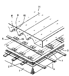
First, FIG. 4 to FIG. 7 are referred and an example of
the flat display device (PDP) according to an embodiment of the
present invention will be described. FIG. 4 is a disassembly
perspective partial view of an example of the flat display
device (PDP). FIG. 5 is a sectional partial view, FIG. 6 is a
perspective partial view, and FIG. 7 is a sectional partial
view.
First, a structure of this flat display device will be
described together with a production method thereof with
CA 02336895 2001-11-16
reference mainly to FIG. 4. For example, the X electrode 2,
which is a first electrode comprised of plural stripe-like
electrodes having a predetermined width, is formed on a rear
side glass substrate 1 such that they are spaced at a
predetermined interval in parallel to each other. This X
electrode 2 is formed by printing conductive paste such as
silver and nickel on the rear side glass substrate 1 through a
screen and then, baking it. This X electrode 2 may be formed by
photo-etching method, thin film method such as vacuum deposition
method or other method.
Next, an insulation layer (composed of low-melting point
material such as glass having a relatively low dielectric
constant) 3 for covering the X electrode 2 and insulating
between the X electrode 2 and a Y electrode 4 which will be
formed later is formed on the rear side glass substrate 1 and
the X electrode 2. This insulation layer 3 is formed by
printing a low-melting point glass paste for example, on the
rear side glass substrate 1 and the X electrode 2 through a
screen and baking it.
The thickness of the insulation layer 3 may be usually
about 0.02-0.03 mm because a withstand voltage of about 200 V is
sufficient if it is intended to insulate an interval between the
X electrode 2 and the Y electrode 4.
However, to block the function of the insulation layer 3
as a dielectric layer for covering the discharge electrode of
CA 02336895 2001-11-16
the AC type PDP, the thickness of the insulation layer 3 is set
to abaut 0.04 mm or more, for example, about 0.04-0.08 mm. If
material having an extremely low dielectric constant is used for
the insulation layer 3 in order to satisfy the condition of the
dielectric layer which does not cause discharge, the thickness
of the insulation layer 3 can be reduced more.
Referring to FIG. 7, the upper Y electrode 4 is disposed
so as to apparently divide the lower X electrode 2. However, if
the insulation layer 3 is treated not to exert the function as a
dielectric layer for covering the discharge electrode of the AC
type PDP, no discharge occurs on the right side of the Y
electrode 4.
Then, an island-like electrode and a conductor for
connecting that island-like electrode to the X electrode 2 which
is the lower electrode will be described with reference to FIGS.
4, 5, 6 as well as FIG. 7. A through hole 5 is made in the
insulation layer 3 near the Y electrode 4 and a column-like, for
example, cylindrical (square pole, rectangular pole and the like
are permitted) conductor 26 is formed in the through hole 5 by
baking conductive paste. Then, the island-like electrode (small
electrode) 6 is formed on the insulation layer 3 such that it is
connected to the conductor 26. This island-like electrode 6 is
formed at the same time as the Y electrode 4. Consequently, the
island-like electrode 6 is electrically connected to the X
electrode 2 through the conductor 26.
CA 02336895 2001-11-16
Meanwhile, the island-like electrode 6 may be formed by
baking conductive paste such as silver, nickel like the X
electrode 2 and Y electrode 6.
As a result, the Y electrode 4 and the island-like
electrode 6 are disposed in parallel on the insulation layer 3.
The surfaces of the Y electrode 4 and island-like electrode 6
are covered by dielectric layer 7.
The dielectric layer 7 is set thinner than the
insulation layer 3, for example, to about 0.01 mm - 0.02 mm so
as to .increase the capacitance, so that it is capable of
accumulating the same wall charge as the ordinary AC type PDP.
Although not shown, protective layer is usually formed on the
surface of the dielectric layer '7 using a material highly
resistant to ion impact having a large secondary electron
emission rate such as magnesium oxide. Discharge is excited
from an electric field shape prior to the discharge as shown by
a discharge path 20.
Next, a structure of the front side glass substrate 11
will be described with reference to FIGS. 4 and 5. The front
side glass substrate 11 has plural grooves 8 formed
corresponding to the X electrodes (first electrodes) 2 on the
rear side glass substrate 1.
It is permissible to form rows of dents instead of the
grooves 8. In this case, plural rows of the dents correspond to
the plural grooves 8. The shape of the dent is, for example, of
CA 02336895 2001-11-16
dome.
This groove 8 can be formed easily by chemical etching
method, sand blast method or the like applied to the front side
glass substrate 11.
The red, green and blue beam producing fluorescent
material layers 9 are formed cyclically in order on an inner
face of each of the plural grooves 8 in the front side glass
substrate 11. The formation of the fluorescent material layers
9 in the groove 8 is carried out by coating with fluorescent
material according to for example, screen printing method.
In case of the dent, the red, green and blue beam
producing fluorescent material layers 9 are formed cyclically in
order on the inner face of each of the plural rows in the front
side glass substrate 11.
The depth of the groove 8 is preferred to be about 0.1 -
0.2 mm. In the normal PDP, the width of the groove 8 is about
0.15 - 0.5 mm. Because the thickness of fluorescent material
layers 9 is about 0.01 mm, the groove 8 is never completely
filled with the fluorescent material. Even if the chemical
etching' method or sand blast methad is used for formation of the
groove 8, generally, the sectional shape of the groove 8 is
substantially inverted U shape as shown in FIG. 5 which makes
advantages for improvement of the luminance and field angle of
the fluorescent material layer 9.
The fluorescent material layers 9 for producing red,
CA 02336895 2001-11-16
green and blue beams, which are primary colors, are formed
directly on the inner face of the groove 8 in the front side
glass substrate 11 or instead, as shown in FIG. 4 and 5 after
forming color filters 10 of red, green and blue, which are
primary colors, on the inner face of the groove 8, corresponding
red, green and blue beam producing fluorescent material layers
are formed on those red, green and blue color filters 10
respectively.
Generally, the color filter 10 can be formed easily by
mixing each pigment with low-melting glass and coloring with
each primary color and then printing through screen or the like.
The front side glass substrate 11 is matched with the
rear side glass substrate 1 and vacuum-sealed with glass frit or
the like. Then, mixed gas suitable for discharge such as neon,
argon and xenon is charged into a space between the both glass
substrates 1 and 11 at an about 0.5 atmospheric pressure.
Consequently, the flat display device is completed.
In the flat type display unit shown in FIGS. 4-7, the X
electrode (first electrode) 2, the insulation layer 3, the Y
electrade (second electrode) 4, the island-like electrode 6, the
dielectric layer 7 and the conductor 26 are provided on the rear
side glass substrate I and the grooves 8 (dent rows may be used
instead), fluorescent material layer 9 and the color filter IO
are provided on the front side glass substrate 11. It is also
permissible to provide the front side glass substrate 11 with
CA 02336895 2001-11-16
the X electrode (first electrode) 2, the insulation layer 3, the
Y electrode (second electrode) 4, the island-like electrode 6,
the dielectric layer 7 and the conductor 26, and the rear side
glass substrate 1 with the grooves 8 {dent rows may be used
instea.d), the fluorescent material layer 9 and the color filters
10.
In the latter case, such components as the electrodes
provided on the front side glass substrate I1 may be formed of
transparent material. However, if the transparency of each
component on the front side glass substrate 11 becomes a problem
when those components are not made of transparent material, the
position of the X electrode 2 is made to correspond to the
partition wall between the groove 8 and the groove 8 formed in
the rear side glass substrate I. Further, a protruding portion
which protrudes up to the through hole 21 which connects the
island-like electrode 6 with the X electrode 2 may be provided
on the X electrode 2.
Next, a flat display device (PDP) according to another
embodiment of the present invention will be described with
reference to a sectional view thereof in FIG. 8. In an example
shown i.n FIG. 8, a through hole 24 which goes through the
island-like electrode 6 and the conductor 26 are formed and the
dielectric layer 7 is formed in the hole 24 too so as to form
so-called hollow electrode 21. Although the island-like
electrode 6 and the X electrode 2, which is the lower electrode,
CA 02336895 2001-11-16
are electrically connected to each other through the conductor
26, the hole 24 is not filled completely with conductive paste
and dielectric layer 7 and is dent-like and further, the
diameter of that dent is of a dimension suitable for generation
of the hollow effect (in ordinary PDP, the diameter is about
0.05 mm). In AC discharge between the Y electrode 4 and the
island-like electrode 6, the hollow effect is generated at a
timing that the island-like electrode 6 is actuated as a
cathode, so that discharge voltage drop and light generation
efficiency increase are found. Here, this hollow electrode 21
functions as a hollow cathode.
Meanwhile, an entire inner peripheral face of this hole
24 may be coated with the dielectric layer 7 and the dielectric
layer 7 does not always have to be applied up to the X electrode
2 at the bottom of the hole 24. That is, the hollow cathode 21
may be actuated as a DC electrode while the island-like
electrode 6 operates as an AC electrode.
If adjacent display cells exist very nearby in case of
the flat display device shown in FIGS. 4-7, so-called cross-
talk, namely, error discharge is likely to occur between the
island-:like electrode 6 and two second electrodes (Y electrodes)
'. 4 located on both sides thereof, so that not only discharge is
generated between adjacent electrodes, but also discharge is
also generated between electrodes located on opposite sides
across the island-like electrode 6. Particularly in a high
CA 02336895 2001-11-16
resolution PDP, its operating voltage range is narrowed.
Then, a flat display device according to still another
embodiment of the present invention, which is an improvement of
the flat display device shown in FIGS. 4-7, will be described
with reference to FIGS. 9-12. FIG. 9 is a perspective partial
view of a flat display device according to still another
embodiment of the present invention. FIG. 10 is a sectional
partial view thereof. FIG. 11 is a plan view showing an
electrode allocation. FIG. 12 is a disassembly perspective
partial view thereof.
First, a structure of the flat display device will be
described together with a production method thereof with
reference to FIGS. 9, 10. The X electrode 2, which is a first
electrode, is formed on the rear side glass substrate 1 so that
plural stripe-like electrodes each having a predetermined width
are disposed in parallel to each other at a predetermined
interval. This X electrode 2 is formed by printing conductive
paste such as silver and nickel on the rear side glass substrate
1 through a screen and then, baking it. This X electrode 2 may
be formed by photo-etching method, thin film method such as
vacuum deposition method or other method.
Next, an insulation layer 3 for covering the X electrode
2 and insulating between the X electrode 2 and a Y electrode 4,
which will be formed later, is formed on the rear side glass
substrate 1 and the X electrode 2. This insulation layer 3 is
CA 02336895 2001-11-16
formed by printing a low-melting point glass paste, for example,
on the rear side glass substrate 1 and the X electrode 2 through
a screen and baking it.
The thickness of the insulation layer 3 may be usually
about 0.02-0.03 mm because a withstand voltage of about 200 v is
sufficient if it is intended to insulate an interval between the
X electrode 2 and the Y electrode 4.
However, to block the function of the insulation layer 3
as a dielectric layer for covering the discharge electrode of
the AC type PDP, the thickness of the insulation layer 3 is set
to about 0.04 mm or more, for example, about 0.04-0.08 mm. If
material having an extremely low dielectric constant is used for
the insulation layer 3 in order to satisfy the condition for the
dielectric layer which does not cause discharge, the thickness
of the insulation layer 3 can be reduced more.
Then, an island-like electrode and a conductor for
connecting that island-like electrode to the X electrode 2 which
is the lower electrode will be described with reference to FIG.
9 as well as FIG. 10. A through hole 5 is made in the
insulation layer 3 near the Y electrode 4 and a column-like, for
example, cylindrical conductor 26 is formed in the through hole
by baking conductive paste. The size and shape of the through
hole 5 are determined depending on electrode width and pixel
pitch. Any shape such as square and rectangle except a circle
is permitted.
CA 02336895 2001-11-16
Then, the island-like electrode 6 is formed on the
insulation layer 3 such that it is connected to the conductor
26. This islandylike electrode 6 is formed at the same time as
the Y electrode 4. Consequently, the island-like electrode 6 is
electrically connected to the X electrode 2 through the
conductor 26. Meanwhile, the island-like electrode 6 may be
formed by baking conductive paste such as silver, nickel like
the X electrode 2 and Y electrode 6.
As a result, the Y electrode 9 and the island-like
electrode 6 are disposed in para1.1e1 on the insulation layer 3.
In this example, the Y electrodes 4 are disposed symmetrically
on the right and left sides of the island-like electrode 6.
Then, the surfaces of the Y electrodes 4 and the island-like
electrode 6 are coated with the dielectric layer 7.
The thickness of the dielectric layer 7 is set smaller
than that of the insulation layer 3, for example, to about 0.01
mm - 0..02 mm so as to increase the capacitance, so that it is
capable of accumulating the same wall charge as the ordinary AC
type PDP. Although not shown, usually, the surface of the
dielectric layer 7 is coated with a material highly resistant to
ion impact having a large secondary electron emission rate such
as magnesium oxide.
As shown in FIG. 10, electric fields 22, 23 of two
dependent display cells 1, 2 are formed between the island-like
electrode 6 and the Y electrodes 4, 4 on both sides thereof.
CA 02336895 2001-11-16
That is, dependent discharge is generated each between the left
half of the island-like electrode 6 and the Y electrode 4 on the
left side and between the right half of the island-like
electrode 6 and the Y electrode 4 on the right side.
FIG. 11 shows a relation of allocation of the X
electrodes 2 (X1, X2, X3, ....), the Y electrode 4 (Y1, Y2, Y3,
....) and the island-like electrode 6 (5112, S212, 5312, ....,
5134, "234, S334, ....).
The Y electrodes Y1, Y2 are disposed on both sides of
each of the island-like electrodes S112, 212, 312, .... and the
Y electrodes Y3, Y4 are disposed on both sides of each of the
island-like electrodes S134, 234, 334, ..... Looking in
different way, the two Y electrodes Y2, Y3 are disposed between
the isJ_and-like electrodes S112, 212, 312, .... and the island-
like electrodes 5134, 234, 334, ..,..
The island-like electrodes S112, 134, .... are disposed
on the X electrode X1. The island-like electrodes 5212, 234,
.... are disposed on the X electrode X2. The island-like
electrodes 5312, 334, .... are disposed on the X electrode X3.
Further, the X electrodes X1, X2, X3, .... are disposed
so as to oppose and intersect the Y electrodes Y1, Y2, Y3, ....
with a predetermined gap.
Next, a structure of the front side glass substrate 11
will be described with reference to FIG. 12. Plural grooves 8
(plural rows of dents may be used instead) are formed in the
CA 02336895 2001-11-16
front side glass substrate 11 corresponding to the X electrodes
(first electrode) 2 on the rear side glass substrate 1.
This groove 8 can be formed easily by chemical etching
method, sand blast method or the like applied to the front side
glass substrate 11.
The red, green and blue beam producing fluorescent
material layers 9 are formed cyclically in order on an inner
face of each of the plural grooves 8 in the front side glass
substrate 11. The formation of the fluorescent material layers
9 in the groove 8 is carried out by coating with fluorescent
material according to for example, screen printing method.
The depth of the groove 8 is preferred to be about 0.1 -
0.2 mm. In the normal PDP, the width of the groove 8 is about
0.15 - 0.5 mm. Because the thickness of fluorescent material
layers 9 is about 0.01 mm, the groove 8 is never completely
filled with the fluorescent material. Even if the chemical
etching method or sand blast method is used for formation of the
groove 8, generally, the sectional shape of the groove 8 is
substantially inverted U shape which makes advantages for
improvement of the luminance and field angle of the fluorescent
material layer 9.
The fluorescent material layers 9 for producing red,
green and blue beams, which are primary colors, are formed
directly on the inner face of the groove 8 in the front side
glass substrate 11 or instead, after forming color filters 10 of
CA 02336895 2001-11-16
red, green and blue, which are primary colors, on the inner face
of the groove 8, corresponding primary colors red, green and
blue beam producing fluorescent material layers 9 are formed on
those red, green and blue color filters 10.
Generally, the color filter 10 can be formed easily by
mixing each pigment to low-melting glass and coloring with each
primary color and then printing through screen or the like.
The front side glass substrate 11 is matched with the
rear side glass substrate 1 and vacuum-sealed with glass frit or
the like. Then, mixed gas suitable for discharge such as neon,
argon and xenon is charged into a space between the both glass
substrates 1 and I1 at an about 0.5 atmospheric pressure.
Consequently, the flat display device is completed.
Next, a modification of the flat display device shown in
FIGS. 9-12 will be described with reference to FTG. I3. If an
area of the island-like electrode 6 is relatively small like a
case of a high resolution PnP, low layer partition walls (for
example, made of an insulator having a low dielectric constant
such as a low-melting glass) 29, which is about 0.02 - 0.03 mm
high, are formed on the dielectric layer 7 corresponding to
substantially the center of the island-like electrode 6 and the
" dielectric layer 7 corresponding to an intermediate between
first and second X electrodes 4 on the right and left sides
respectively of the island-like electrode 6 in order to separate
the adjacent discharge cells clearly, such that these partition
CA 02336895 2001-11-16
walls are extended in an extending direction of the X electrodes
2. Consequently, the island-like electrodes 6 can be separated
more clearly from a viewpoint of structure, so that the
operating range is expanded and cross-talk between adjacent
display cells can be decreased.
Further, by providing the grid-like partition wall 29
for surrounding each display cell on the dielectric layer 7 as
shown in FIG. 14, the cross-talk between adjacent display cells
can be reduced.
Usually,a screen of every display device is composed of
light producing portion and non-light producing portion and by
coloring the non-light producing portion with black, the
contrast ratio is increased.
However, the front side glass substrate 11 of the above
described flat display device (PDP) has a small non-light
producing portion relative to coated area of the fluorescent
material layer, which is the light producing portion. For the
reason, there is a problem about the contrast ratio.
Acceleration and stabilization of so-called address
discharge are very important for attaining high resolution in
the PDP having any structure. It has been well known that in
the PDP, supplying charged particles or quasi-stable atoms,
which tell the start of discharge, namely so-called priming to
discharge cells is an effective way for reducing discharge delay
time and stabilizing the operation.
CA 02336895 2001-11-16
However, because in the conventional PDP, light emission
of this auxiliary discharge reduces the contrast of a screen and
for other reasons, an effective, simple-structure auxiliary
discharge mechanism has not been achieved.
A structure of the glass substrate in which the above
described problems have been solved will be described with
reference to a perspective view shown in FIG. 15. Reference
numeral 11 denotes a glass substrate (although it is a front
side glass substrate here, it may be a rear side glass
substrate). Then, plural grooves 8 each having a concave curved
face (plural rows of dents may be used instead) are provided in
the front side glass substrate 11 such that they have the same
width, depth and shape (for example, U-letter shaped in
sectior.~) .
The grooves 8 are formed by applying the sand blast
method, chemical etching method or the like to the front side
glass substrate 11. Meanwhile, reference numeral 8HR denotes
partition wall between the adjacent grooves 8.
Black layer (for example, black glass layer) BL, red
light producing fluorescent material layer 9R, green light
producing fluorescent material layer 9G and blue light producing
fluorescent material layer 9B are formed cyclically in order in
each of the plural grooves (plural rows of dents may be used
instead) by coating.
Because three neighboring grooves 8 having the red,
CA 02336895 2001-11-16
green and blue light producing fluorescent material layers 9R,
9G, 9B compose a single color pixel, the groove 8 having the
black layer HL as if it separates these color pixels improve the
contrast ratio of the color image composed of many color pixels.
Although there is a tear that lights from the respective
color fluorescent material layers 9R, 9G, 9H in the plural
grooves 8 diffuse to mix with each other to some extent, an
existence of the concave curved face groove 8 coated with the
black layer has an effect of reducing the mixing of the colors
as well as improving of the contrast ratio.
If the groove 8 coated with the black layer BL is
disposed between neighboring grooves 8 coated with the
respective fluorescent material layers 9R, 9G, 9B or between
neighboring two grooves 8, the contrast ratio of the color image
is improved further.
Although in this example, the width of the groove 8
coated with the black layer BL is the same as the width of each
of the grooves 8 coated with the respective color fluorescent
material layers 9R, 9G, 9B, it does not always have to be the
same. That is, the width of the groove 8 coated with the black
layer HL may be larger or smaller than the width of each of the
grooves 8 coated with the respective color fluorescent material
layers 9R, 9G, 9B.
Although in this example, the width of the groove 8
coated with each color fluorescent material layer 9R, 9G, 9B is
CA 02336895 2001-11-16
the same, it does not always have to be the same. It is
permissible to change the width of the groove 8 coated with each
color fluorescent material layer 9R, 9G, 9H for each color so as
to adjust color balance.
A structure of a flat display device containing the
front side glass substrate 11 shown in FIG. I5 will be described
with reference to a disassembly perspective partial view of FIG.
16. For example, the X electrode 2, which is a first electrode,
is formed on the rear side glass substrate 1 so that plural
stripe-like electrodes each having a predetermined width are
disposed in parallel to each other at a predetermined interval.
This X electrode 2 is formed by printing conductive paste such
as silver and nickel on the rear side glass substrate 1 through
a screen and then, baking it. This X electrode 2 may be formed
by photo-etching method, thin film method such as vacuum
deposition method or other method.
Next, an insulation layer 3 for covering the X electrode
2 and insulating between the X electrode 2 and a Y electrode 4,
which will be formed later, is formed on the rear side glass
substrate 1 and the X electrode 2. This insulation layer 3 is
formed by printing a low-melting point glass paste, for example,
on the .rear side glass substrate 1 and the X electrode 2 through
a screen and baking it.
The thickness of the insulation layer 3 may be usually
about 4.02-0.43 mm because a withstand voltage of about 200 V is
CA 02336895 2001-11-16
sufficient if it is intended to insulate an interval between the
X elect:rode 2 and the Y electrode 4.
However, to block the function of the insulation layer 3
as a dielectric layer for covering the discharge electrode of
the AC type PDP, the thickness of the insulation layer 3 is set
to about 0.04 mm or more, for example, about 0.04-0.08 mm. If
material having an extremely low dielectric constant is used for
the insulation layer 3 in order to satisfy the condition for the
dielectric layer which does not cause discharge, the thickness
of the insulation layer 3 can be reduced more.
Although FIG. 16 shows a case where the front side glass
substrate 11 of FIG. 15 is applied to the front side glass
substrate 11 of the flat display device, it is permissible to
form the above described plural grooves 8 in the rear side glass
substrate 1 and then form the black layer HL, the red
fluorescent material layer 9R, the green fluorescent material
layer 9G and the blue fluorescent material layer 9H cyclically
in order in each of the plural grooves 8 (plural rows of dents
may be used instead).
In this case, the X electrodes 2, the Y electrodes 4 and
the island-like electrodes 6 are disposed on the front side
~~ glass substrate 11 so as to form a reflection fluorescent face
type, double-electrode discharge PDP.
Next, a modification of the flat display device of FIG.
17 will be described. Although the island-like electrode 6 for
CA 02336895 2001-11-16
discharge corresponding to each of the grooves 8 (plural rows of
dents may be used instead) coated with the black layer HL is not
formed as shown in FIG. 16, it is permissible to form the
auxiliary discharge island-like electrode 27 in this portion as
shown .in FIG. 17. This auxiliary discharge island-like
electrode 27 is not restricted to the AC type, but may be so-
called DC type electrode whose surface is not coated with the
dielectric layer. Because light produced by the auxiliary
discharge island-like electrode 27 does not go out of the groove
8 coated with the black layer HL, there is no fear that the
contrast of the screen is reduced. Because the auxiliary
discharge by this auxiliary discharge island-like electrode 27
is always turned on irrespective of the image signal, effective
priming can be always supplied to pixels adjacent the auxiliary
discharge cell.