Some of the information on this Web page has been provided by external sources. The Government of Canada is not responsible for the accuracy, reliability or currency of the information supplied by external sources. Users wishing to rely upon this information should consult directly with the source of the information. Content provided by external sources is not subject to official languages, privacy and accessibility requirements.
Any discrepancies in the text and image of the Claims and Abstract are due to differing posting times. Text of the Claims and Abstract are posted:
| (12) Patent Application: | (11) CA 2337062 |
|---|---|
| (54) English Title: | BALLAST FOR AT LEAST ONE GAS DISCHARGE LAMP, AND A METHOD FOR OPERATING SUCH A BALLAST |
| (54) French Title: | BALLAST POUR AU MOINS UNE LAMPE A DECHARGE, ET PROCEDE POUR FAIRE FONCTIONNER UNE TEL BALLAST |
| Status: | Deemed Abandoned and Beyond the Period of Reinstatement - Pending Response to Notice of Disregarded Communication |
| (51) International Patent Classification (IPC): |
|
|---|---|
| (72) Inventors : |
|
| (73) Owners : |
|
| (71) Applicants : |
|
| (74) Agent: | SMART & BIGGAR LP |
| (74) Associate agent: | |
| (45) Issued: | |
| (86) PCT Filing Date: | 2000-04-19 |
| (87) Open to Public Inspection: | 2000-11-23 |
| Examination requested: | 2005-02-02 |
| Availability of licence: | N/A |
| Dedicated to the Public: | N/A |
| (25) Language of filing: | English |
| Patent Cooperation Treaty (PCT): | Yes |
|---|---|
| (86) PCT Filing Number: | PCT/DE2000/001226 |
| (87) International Publication Number: | DE2000001226 |
| (85) National Entry: | 2001-01-10 |
| (30) Application Priority Data: | ||||||
|---|---|---|---|---|---|---|
|
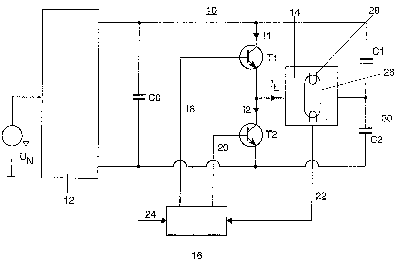
The present invention relates to a ballast for at least one gas discharge lamp
(26). Said ballast comprises an inverter that is fed by a direct current
source (C0). The inverter is provided with a bridge circuit with a first and a
second controllable switch (T1, T2). The bridge circuit is arranged parallel
in relation to the direct current source (C0). The bridge centre is connected
to a load circuit (14) which comprises the at least one gas discharge lamp
(26). Each gas discharge lamp (26) is provided with a first and a second
electrode (28, 30). The ballast also comprises a control circuit (16) by means
of which the pulse duty factor of the first and second switch (T1, T2) can be
influenced. The pulse duty factor is unequal 50 % and can be controlled by
means of the control circuit in such a way that the first and second electrode
are thermally charged in an essentially equal manner on average. The invention
further relates to a corresponding method for operating a ballast for at least
one gas discharge lamp.
L'invention concerne un ballast pour au moins une lampe à décharge (26), comprenant un convertisseur alimenté par une source de tension continue (C0) présentant un circuit en pont avec un premier et un deuxième interrupteurs réglables (T1, T2), monté en parallèle avec ladite source de tension continue (C0), le centre du pont étant connecté à un circuit de charge (14) comprenant au moins une lampe à décharge (26), chaque lampe à décharge (26) présentant une première et une deuxième électrodes (28, 30), et un circuit de commande (16) influençant le taux d'impulsions du premier et du deuxième interrupteurs (T1, T2), ce taux d'impulsions étant différent de 50 %. L'invention est caractérisée en ce que le taux d'impulsions est réglable au moyen du circuit de commande, de telle façon que la première et la deuxième électrodes soient, en moyenne, thermiquement chargées de façon sensiblement égale. L'invention concerne en outre un procédé correspondant pour faire fonctionner un ballast pour au moins une lampe à décharge.
Note: Claims are shown in the official language in which they were submitted.
Note: Descriptions are shown in the official language in which they were submitted.
2024-08-01:As part of the Next Generation Patents (NGP) transition, the Canadian Patents Database (CPD) now contains a more detailed Event History, which replicates the Event Log of our new back-office solution.
Please note that "Inactive:" events refers to events no longer in use in our new back-office solution.
For a clearer understanding of the status of the application/patent presented on this page, the site Disclaimer , as well as the definitions for Patent , Event History , Maintenance Fee and Payment History should be consulted.
| Description | Date |
|---|---|
| Application Not Reinstated by Deadline | 2010-09-13 |
| Inactive: Dead - Final fee not paid | 2010-09-13 |
| Deemed Abandoned - Failure to Respond to Maintenance Fee Notice | 2010-04-19 |
| Deemed Abandoned - Conditions for Grant Determined Not Compliant | 2009-09-14 |
| Notice of Allowance is Issued | 2009-03-13 |
| Letter Sent | 2009-03-13 |
| Notice of Allowance is Issued | 2009-03-13 |
| Inactive: Approved for allowance (AFA) | 2009-03-11 |
| Amendment Received - Voluntary Amendment | 2008-11-24 |
| Inactive: S.30(2) Rules - Examiner requisition | 2008-06-03 |
| Inactive: IPC from MCD | 2006-03-12 |
| Inactive: IPC from MCD | 2006-03-12 |
| Letter Sent | 2005-02-11 |
| Request for Examination Requirements Determined Compliant | 2005-02-02 |
| All Requirements for Examination Determined Compliant | 2005-02-02 |
| Request for Examination Received | 2005-02-02 |
| Inactive: Cover page published | 2001-04-20 |
| Inactive: First IPC assigned | 2001-04-10 |
| Inactive: Notice - National entry - No RFE | 2001-03-26 |
| Letter Sent | 2001-03-26 |
| Inactive: Applicant deleted | 2001-03-26 |
| Application Received - PCT | 2001-03-20 |
| Application Published (Open to Public Inspection) | 2000-11-23 |
| Abandonment Date | Reason | Reinstatement Date |
|---|---|---|
| 2010-04-19 | ||
| 2009-09-14 |
The last payment was received on 2009-03-04
Note : If the full payment has not been received on or before the date indicated, a further fee may be required which may be one of the following
Patent fees are adjusted on the 1st of January every year. The amounts above are the current amounts if received by December 31 of the current year.
Please refer to the CIPO
Patent Fees
web page to see all current fee amounts.
| Fee Type | Anniversary Year | Due Date | Paid Date |
|---|---|---|---|
| Basic national fee - standard | 2001-01-10 | ||
| Registration of a document | 2001-01-10 | ||
| MF (application, 2nd anniv.) - standard | 02 | 2002-04-19 | 2002-04-03 |
| MF (application, 3rd anniv.) - standard | 03 | 2003-04-21 | 2003-04-03 |
| MF (application, 4th anniv.) - standard | 04 | 2004-04-19 | 2004-03-31 |
| Request for examination - standard | 2005-02-02 | ||
| MF (application, 5th anniv.) - standard | 05 | 2005-04-19 | 2005-03-31 |
| MF (application, 6th anniv.) - standard | 06 | 2006-04-19 | 2006-04-03 |
| MF (application, 7th anniv.) - standard | 07 | 2007-04-19 | 2007-03-14 |
| MF (application, 8th anniv.) - standard | 08 | 2008-04-21 | 2008-03-12 |
| MF (application, 9th anniv.) - standard | 09 | 2009-04-20 | 2009-03-04 |
Note: Records showing the ownership history in alphabetical order.
| Current Owners on Record |
|---|
| PATENT-TREUHAND-GESELLSCHAFT FUER ELEKTRISCHE GLUEHLAMPEN MBH |
| Past Owners on Record |
|---|
| FRANZ RAISER |

