Note: Descriptions are shown in the official language in which they were submitted.
CA 02337154 2001-O1-11
WO 00/72239 PCT/GB00/01550
1
Detector Constructed From Fabric
Reference to Related Applications
The present invention was made by Mr David Lee Sandbach who is
resident in the United Kingdom. A permit to file a first application outside
the
United Kingdom under Section 23(1 ) of the Patent Act 1977 was obtained on
19 May 1999. The present application claims priority from United States
patent application number 091315,139. With respect to the United State's
designation, the present application is filed as a continuation-in-part.
Field of the Invention
The present invention relates to a position sensor for detecting the
position of a mechanical interaction.
Background of the Invention
A position sensor for detecting the position of a mechanical interaction
is disclosed in European Patent publication 0 989 509, equivalent to United
States patent application 09/298,172, Korean patent application number 99-
40363, Japanese patent application number 11-272,513 and Australian
2o patent application 48770/99, all assigned to the present Assignee. The
position detector is configured to determine the position of a mechanical
interaction. In addition, the detector is also configured to measure the
extent
of a mechanical interaction in which said representation of the extent of a
mechanical interaction is usually made up from components representing the
force of the mechanical interaction and the area over which the mechanical
interaction takes effect.
A problem with the known position sensor disclosed in the aforesaid
patent applications is that it is possible for incorrect measurements to be
obtained if the detector is folded in certain orientations. Thus, with the
known
CA 02337154 2001-O1-11
WO 00/72239 PCT/GB00/01550
2
detector, satisfactory results are obtained if the detector is placed over a
flat
surface, such as a desk or table etc. However, if the detector is folded over
a
curvilinear surface, it is possible for erroneous results to be obtained at
positions where the detector is folded.
s The known detector is fabricated from two conducting layers of fabric
with a non-conducting layer positioned therebetween. In order to reduce
occurrences of erroneous results, due to folding, it is known to strengthen
and thicken the intermediate non-conducting layer. However, when the
intermediate layer is strengthened in this way, the response of the detector
o changes in that it becomes less sensitive to mechanical interactions. Thus,
if
a mechanical interaction takes the form of a manual operation of a finger
upon the detector, for example in order for a position to be determined from
which action can then follow, it becomes difficult for the detector to k~e
pressed manually. Similarly, if the intermediate layer is modified so as to
~5 make mechanical interactions easier to accomplish, there is then a greater
likelihood that erroneous contact may result.
Brief Summary of the Invention
According to an aspect of the present invention, there is provided a
2o position sensor for detecting the position of a mechanical interaction,
including: a first fabric layer having electrically conductive fibres machined
therein to provide a first conductive outer layer allowing conduction in all
directions along said first layer; a second fabric layer having electrically
conductive fibres machined therein to provide a second conductive outer
2s layer allowing conduction in all directions along said second layer; a
central
layer disposed between said first outer layer and said second layer, said
central layer including conducting means; a first insulating separating means
disposed between said first conductive outer layer and said conducting
means; and a second insulating separating means disposed between said
CA 02337154 2001-O1-11
wo oonz~s pcricBOOioisso
3
second conductive outer layer and said conducting means; wherein said
conducting means provides a conductive path between said first conducting
outer layer and said second conducting outer layer at a position of a
mechanical interaction.
Brief Description of the Several Views of the Drawings
Figure A illustrates a known position sensor as described in the prior
art;
Figure 1 shows a position sensor embodying the present invention;
1o Figure 2 details the sensor shown in Figure 1;
Figure 3 illustrates upper and lower fabric layers of the sensor shown
in Figure 2;
Figure 4 shows an alternative embodiment of that shown in Figure 3T
Figure 5 shows a portion of the sensor shown in Figure 2, in cross
section;
Figure 6 shows a cross-sectional view of a preferred embodiment;
Figure 7 shows a cross-sectional view of a first alternative
embodiment;
Figure 8 shows a cross-sectional second alternative
view of a
2o embodiment;
Figure 9 shows a cross-sectionalview a third alternative
of
embodiment;
Figure 10shows a cross-sectionalview a fourthalternative
of
embodiment;
Figure 11shows a cross-sectionalview a furtherpreferred
of
embodiment;
Figure 12shows a cross-sectionalview a furtheralternative
of
embodiment
Figure 13shows a cross-sectionalview a furtheralternative
of
CA 02337154 2001-O1-11
WO 00/72239 PCT/GB00/01550
4
embodiment;
Figure 14 shows a detector for detecting force and area separately;
Figures 15A, 15B, 15C and 15D illustrate procedures for measuring
the position of a force applied to the position sensor;
Figure 16 shows an interface circuit of the type identified in Figure ?;
Figure ? 7 illustrates a program executed by the interface circuit shown
in Figure 16;
Figure ?8 details a portion of the procedure identified in Figure ?7;
Figure ?9 details a further procedure identified in Figure ?7; and
Figure 20 details a further procedure ident~ed in Figure 17.
Best Mode for Carrying Out the Invention
A position sensor of the type described by the prior art is illustrated
in the cross-sectional view shown in Figure A. The sensor has conductive
outer layers of fabric A01 and A02, separated by an insulating layer A03.
The purpose of the insulating layer is to prevent electrical contact between
the outer layers A01 and A02, except at positions of mechanical interaction.
For example, at location A04 a force, indicated by arrow A05, presses the
sensor against a solid surface A06. The layers are thus pressed into
2o intimate contact and due to the open structure of the insulating layer A03,
the outer layers come into contact with each other.
By applying electrical potential gradients across outer Layer A01 and
measuring the electrical potential of outer layer A02, the location of the
mechanical interaction may be determined. In addition, by measuring the
2s current flowing to the outer layer A02, an indication of the size of force
A05,
or, alternatively, the area over which it applies a pressure to the sensor,
may be determined.
A fold A07 in the sensor exemplifies a problem with this type of
sensor. The outer layer A01, on the inside of the fold becomes compressed
CA 02337154 2001-O1-11
wo ooniZ39 Pcricsooioisso
and pushes out against the insulating layer A03. In addition, due to the
open structure of the insulating layer, the layer A01 pushes out against the
outer layer A02, and thereby produces an electrical contact A08 between
the conducting layers. The electrical contact A08 influences the positional
5 voltage measurement and cun-ent measurement, and thereby leads to
incorrect interpretation of the position and area/force of the mechanical
interaction at location A04.
A position sensor 101 embodying the present invention is shown in
Figure 1, fabricated from the fabric layers of material and configured to rest
on flat and curvilinear surfaces. The sensor responds to mechanical
interactions and in the specific application shown in Figure 1, these
mechanical interactions take the form of manual pressure being applied by
users in order to make selections.
In the example shown in Figure 1, the sensor 101 provides a
~5 substitute for a television, video recorder or satellite television remote
control. In preference to a solid object providing a series of buttons, the
detector is substantially fabric and may adopt a shape defined by soft
furnishing. In the example shown, the detector 101 is shown as a separate
item but in an alternative configuration, the detector could be included as
2o part of soft furnishing, such as sofa 102.
The sensor 101 includes an interface circuit 103 arranged to respond
to mechanical interactions and to provide co-ordinate and pressure data
over an interface line 104 to a processing device 105. In response to
mechanical interactions effected by a user, positional data is conveyed to
25 processing circuit 105 that in turn transmits infra-red data via an infra-
red
transmitter 106 to audio visual equipment, such as television 107.
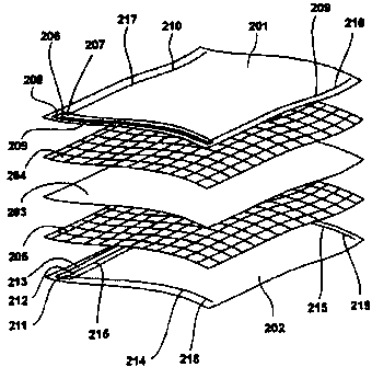
An example of a sensor of the type shown in Figure 1 is shown in~the
exploded view of Figure 2. The sensor comprises of two woven outer fabric
layers 201 and 202, separated by a central layer 203. The central layer 203
CA 02337154 2001-O1-11
WO 00/72239 PGT/GB00/OI550
6
is a layer of knitted fabric which may be made from conductive fibre only.
Such fibre may, for example, be a carbon coated nylon fibre. However,
preferably a yam is used in the knit which is a mixture of insulating and
conductive fibres and such a central layer is described later with respect to
~ Figure 9.
A first insulating mesh layer 204 is located between the upper fabric
layer 201 and the central layer 203, and a second insulating mesh layer 205
is located between the lower fabric layer 202 and the central layer 203. The
insulating mesh layers 204 and 205 are made from polyester fabric of a warp
knit constnrction. Fabric of this type is readily available and may be used in
applications such as mosquito nets.
Electrically conductive fibres are used when weaving layer 201 and
202, and so the layers 201 and 202 define two electrically conductive layers.
Alternatively, the layers 201 and 202 may be constructed from non-woven
~5 (felted), or knitted fabrics or a composite structure. However, in each
alternative case, electrically conductive fibres are included in the
production
of the fabric, thus providing electrically conductive layers.
Two electrical connectors 206 and 207 are located on a rectangular
insulating stripe 208 that is positioned along one edge of fabric layer 201.
2o The insulating stripe is produced by printing insulating ink onto the
fabric but
alternatively may be an insulating adhesive tape. The connectors 206 and
207 provide a means of connection from the interface circuit 203 to low
resistance elements 209 and 210 respectively. The low resistance elements
209 and 210 are fabricated from fabric coated with metals such as nickel or
25 silver. Material of this type is readily available and is used for
shielding
equipment from electromagnetic interference. The low resistance elements
are attached to the conductive fabric layer 201 and the insulating stripe X08
by a conductive adhesive, such as a pressure sensitive acrylic adhesive
containing metallised particles. Therefore, portions 216 and 217 of the low
CA 02337154 2001-O1-11
WO OOI72Z39 PGT/GB00/01550
7
resistance elements 209 and 210 make electrical contact with the conductive
fibres of layer 201 along two of its opposing edges. The conductive adhesive
ensures a bond is formed between the low resistance elements 209 and 210
and the conductive fibres. Due to the bond, the resistance between the
conductive fibres and the contacting portions 216 and .217 remains
unaffected by folding or flexing the layer 201. This is important, as
otherwise
a 'dry joint' would exist connecting 216 and 217 to 201, and a varying
resistance at the connections would lead to unreliable and, possibly, unstable
measurements when the sensor is operated.
Alternatively, the low resistance elements 209 and 210 are formed by
attaching, e.g. by sewing on, a low resistance fibre to the layer 201 and then
printing a conductive adhesive or compound onto it and the layer 201.
Alternatively the low resistance elements may be produced by printing an
elastomeric material containing conductive particles onto the layer 201. All
of
~5 the alternative described methods provide a suitable bond, forming a
reliable
electrical connection or 'wet joint'.
The lower fabric layer 202 has a similar construction to the
upper fabric layer 201, having connectors 211 and 2'12 located on insulating
stripe 213. The connectors 211 and 212 providing a means for connecting
2o the interface circuit 103 with low resistance elements 214 and 215
respectively. The two layers 201 and 202 are rectangular and the
construction of layer 202 is rotated ninety degrees from that of layer 201.
Thus contacting portions 216 and 217 contact the conductive fibres in layer
201 along two opposing edges, and the low resistance elements 214 and
25 215 have contacting portions 218 and 219 which contact the conductive
fibres in layer 202 along the alternate opposing edges.
The upper and lower fabric layers 201 and 202 are shown separately
in Figure 3. Fabric layers 201 and 202 are plain weaves having conductive
fibres in both the warp and the weft directions and so are conductive in all
CA 02337154 2001-O1-11
wo oonaz39 PcricBOOroisso
8
directions along the respective layers. In Figure 3, the warp fibres 301 of
layer 201 are shown approximately horizontal and extend between the two
contacting portions 216 and 217, while the weft fibres 302 are parallel to the
contacting portions 216 and 217 and are shown approximately vertical. In
layer 202, the warp fibres 301 are shown approximately vertical and extend
between the contacting portions 218 and 219, while the weft fibres 302 are
parallel to the contacting portions 218 and 219 and are shown approximately
horizontal.
It is advantageous to the operation of the sensor, when current
o measurements are made, if the layers 201 and 202 have anisotropic
conductivity. In particular it is advantageous if the layers 201 and 202 are
more conductive in the directions parallel to their respective contacting
portions. Thus, when the sensor is operated and a voltage gradient is applied
between a pair of contacting portions, the respective layer is most conductive
~5 ' in a direction perpendicular to the voltage gradient and less conductive
parallel to the voltage gradient. To achieve the desired anisotropic
conductivity, the warp fibres are chosen to be of a higher resistance than the
weft fibres. For this reason, the warp fibres 301 are 24 decitex carbon coated
nylon 6 fibres sold by BASF and identified by the designation F901, such
20 carbon coated fibres are commonly available and are used in electrostatic
dissipation applications. The weft fibres are 16 decitex monofilament fibres,
electrochemically coated with nickel and/or silver, sold under the trade mark
"Xstatic" by Sauquoit Industries Inc., Pennsylvania, USA. Similar metallised
fibres are commonly available and are normally used in electromagnetic
25 interference shielding. Thus, a typical resistivity for a weft fibre is
500ohms
per centimetre, as opposed to approximately 200Kohms per centimetre for
the warp fibre. In layers 201 and 202 the fabric is woven with the same
average spacing of 7.3 fibres per millimetre for both the weft and warp.
Therefore, due to the different resistivity of the warp and weft fibres, the
sheet
CA 02337154 2001-O1-11
WO 00/72239 PC'f/GBOO/OI550
9
resistivity of the layers in the directions parallel to the contacting
portions is
approximately 400 times less than the sheet resistivity in the perpendicular
direction.
In an alternative embodiment the outer fabric layers 201 and 202 are
s replaced by outer fabric layers 401 and 402 respectively as shown in Figure
4. The construction of layers 401 and 402 is similar to that of layers 201 and
202, except for the type of fibres used in the weft and warp. Thus, contacting
portions 403 and 404 are located along opposing edges of layer 401 and
contact conductive fibres within said layer, while contacting portions 405 and
~0 406 are located along the alternate opposing edges of the layer 402 and
make electrical contact with conductive fibres within layer 402.
Outer layer 401 includes conductive fibres 407 that conduct in the
direction of the current flowing from contacting portion 403 to contacting
portion 404. Cross threads 408 conduct in a direction perpendicular to this
~ s ~ one, and have the effect of ensuring a linear voltage gradient across
the
sheet, even when the resistance of connections between lateral fibres 407
with the contacting portion 403 and 404 are variable, as would be expected in
a manufacturing process. Insulating fibres 409 are used between adjacent
parallel conductive fibres 407 in the warp direction and between adjacent
2o parallel conducting fibres 408 in the weft direction. Anisotropic
conductivity is
achieved, in the present embodiment, by selecting a different ratio of
conductive fibres 407 and 408 to non-conductive fibres 409 for each of the
warp and weft directions. Thus, in the direction perpendicular to the
contacting portions 403 and 404, which is horizontal in the drawing of layer
25 401 shown in Figure 4, an insulating fibre alternates with a conducting
fibre
402. There is an equal quantity of both. However, in the perpendicular
direction, there are two conducting fibres 408 for each parallel insulating
fibre
409. Thus, when the sensor is operated, in the direction perpendicular to
applied current flow, or the direction perpendicular to the voltage gradient,
CA 02337154 2001-O1-11
WO 00!12239 PCT/GB00/01550
conductivity is increased.
Outer fabric layer 402 has a similar structure to layer 401 but is rotated
through ninety degrees. Therefore the weave includes weft fibres which are
substantially parallel to contacting portions 405 and 406 and warp fibres
5 which are perpendicular to contacting portions 405 and 406. Tk~e layer 402
is
anisotropic in a similar manner to layer 401, since its weave contains two
conductive fibres 408 for every insulating fibre 409 in the weft, while
containing an equal number of conducting fibres 407 to insulating fibres 409
in the warp.
~o In the present embodiment, the conductive fibres 407 and 408 in both
the weft and warp directions may be of equal resistivity since the anistropic
conductivity of the layers is achieved by selection of the ratios of
conductive
fibres to insulating fibres. Therefore, a similar carbon coated nylon fibre
may
be used in both the weft and the warp directions of the weave.
~ 5 A portion of the sensor shown in Figure 2 is shown in the cross-
sectional view of Figure 5. The spaces between the layers are shown
exaggerated in this Figure, and the following Figures, in order to provide
clarity. A force indicated by arrow 501 is pressing the sensor at position 502
against a solid surface 503. At position 502 the outer fabric layers 201 and
202 are pressed against the respective mesh layers 204 and 205. Also, due
to the open structure of the mesh, the outer fabric layers are able to make
contact with the central layer 203 through the apertures in the mesh and,
moreover, the conductive fibres in the outer fabric layers make electrical
contact with the conductive fibres included in the central layer. Thus, the
conductive fibres in the central layer present a conducting means which
provide a conductive path between the outer conductive fabric layers 201
and 202 at the position of the mechanical interaction.
In an alternative embodiment where the current measurement
accuracy is not critical, costs savings are made by reducing the proportion of
CA 02337154 2001-O1-11
WO 00/72239 PCT/GB00101550
11
the conductive fibre to insulating fibre used in the outer layers,
particularly by
reducing the conductive fibre content in the direction parallel to the
contacting
portions.
The knitted central layer 203 has a compressible structure which
becomes more conductive (less resistive) when it is compressed. This is due
to loops in the conductive fibre coming increasingly into contact with other
such loops as they are pressed together. As a result of this, the resistance
between the outer layers at location 502 decreases as the force, indicated by
arrow 501, increases. In addition, if the pressure applied to the sensor at
~o location 502 is kept constant but the area over which it is applied is
increased, then the resistance between the outer layers decreases, due to
the increasing number of conducting fibres in the central layer coming into
contact with the outer layers.
The sensor shown in Figure 5 is folded at location 504 resulting in a
~5 tendency for one of the conducting layers to be brought into contact with
the
central layer. A property of many fabrics is that they may stretch in response
to tensional forces but they may be compressed less easily in response to
compressive forces. Consequently, rather than being compressed as such,
fabrics tend to fold and bunch at positions where compressive force is being
2o applied.
Certain constructions of fabric behave in the opposite way, being more
easily compressed than stretched and in this case electrical contact at
location 505 is made between the central layer 203 and the outer layer 201.
In practice it is extremely rare for contact due to such compression and
25 extension forces to occur simultaneously on both sides of the central layer
at
the location of a fold.
In the situation shown in Figure 5, a fold has been created at position
504. In response to this fold, the outer circumferences of the fabric assembly
will tend to be in tension and will therefore stretch, with the inner
CA 02337154 2001-O1-11
wo oonz~9 rcncaooioisso
12
circumferences of the fabric assembly being in compression, resulting in
bunching. This bunching will in tum cause radial force outwards, thereby
tending to cause its outward circumferences to come into contact with inner
circumferences of adjoining layers. Compression forces are therefore applied
s and hence bunching occurs towards the inside of a fold.
As shown in Figure 5 conducting layer 202 has been brought into
contact at location 505 with central layer 203 through insulating layers 205.
As a result of this folding, electrical contact occurs where these two layers
are
brought into contact. However, a similar contact does not occur between
~o central layer 203 and conductive layer 201. Consequently, although
conduction occurs between conducting layer 202 and central layer 203, there
is no similar conduction between central layer 203 and conductive layer 201
such that the presence of the fold does not result in spurious output signals:
Thus, the application of force, indicated by arrow 501, does result in all
~ 5 of the conductive layers being brought into contact such that current may
flow
between the layers to which voltage has been applied. However, when a
sharp fold is introduced into the detector, as illustrated at 504, it is only
possible for conduction to occur between two of the layers. Consequently,
insulation still exists between the central layer and the other outer layer
such
2o that this is not interpreted as an application of force or similar
mechanical
interaction of interest.
in theory, it is possible for a fold to result in current being transmitted
along the central layer 203 to an actual point of mechanical interaction. For
this reason, it is preferable for the central layer 203 to have relatively low
2s conductivity along the layer compared with conductivity across its
thickness.
This is further improved if the central layer 203 has a characteristic such
that
its conductivity significantly increases when the material is placed under
pressure. Thus, a compressed portion at a position of a mechanical
interaction will tend to have a relatively low resistance. This compares with
CA 02337154 2001-O1-11
WO 00/72239 PCT/GB00/01550
13
the uncompressed central layer which will tend to have a much higher
resistance. This, in combination with the relative length of the central layer
between the position of a fold and the position of a mechanical interaction,
will ensure that the degree of current being transmitted in this way is
relatively
s small compared to the degree of cun-ent being transmitted at an actual
mechanical interaction.
A portion of the position sensor of the prefer-ed embodiment is shown
in the cross-sectional view of Figure 6. The outer fabric conducting layers
201
and 202 and the central layer 203 are of the same type as those described
o with reference to Figures 2 and 3. However, in this embodiment an array of
insulating adhesive dots 601 provides the insulating separating means
between the outer layer 201 and central layer 203, and a similar array of dots
provides the insulating separating means between the outer layer 202 and
central layer 203. The insulating adhesive is a polyurethane adhesive
~5 available from Penn Nyla, of Nottingham, Great Britain, but similar
materials,
of different qualities, are commonly available from a variety of
manufacturers.
Such adhesives are commonly used as continuous layer laminates, for
waterproofing fabrics. The adhesive is applied by mixing with a solvent and
printing the liquid solution. The adhesive is then heat cured after the layers
2o are assembled.
The array of adhesive dots provide the same insulating function as the
previously described mesh layers but also serve to attach the layers to their
adjacent layer or layers. Thus, no further lamination process is required.
Alternatively, the adhesive dots may be replaced by stripes of
25 adhesive, or a network of lines of adhesive.
A portion of an alternative position sensor 701 embodying the present
invention is shown in the cross-sectional view of Figure 7. The sensor~has
two outer layers 702 and 703 separated by a central layer 203 of the type
previously described with reference to Figure 2. The outer layers 702 and
CA 02337154 2001-O1-11
wo oonia~9 rcricBOOioisso
14
703 are woven using alternating strands of insulating yarn 704 and
conductive fibre 705 in both the warp and the weft. The non-conducting yam
704 is of a larger diameter than that of the conductive fibre 705 and so the
conductive fibre is recessed below the general surface of the layers 702 and
703. The recessing of the conductive fibre 705 is further enhanced by using a
single filament fibre of carbon coated nylon 6, while the insulating yam is
made by twisting together a bundle of fine insulating fibres of polyester,
each
of which is of a thinner diameter than the conductive fibre. The conductive
fibre is therefore considerably less compressible and flexible than the
o insulating yam and so it tends to remain straighter than the insulating yam
in
the woven fabric.
The conductive fibre 705 in the warp and the weft of the layer 702 thus
forms a conductive layer which allows conduction in all directions along the
layer 702. The conductive layer so formed, is recessed from the conductive
~5 fibre in the central layer by means of the insulating yam 704. The
conductive
layer becomes exposed at the surfaces of the layer upon application of
pressure. The insulating yarn therefore provides an insulating separating
means between the conductive layer within layer 702 and the conducting
fibre in the central layer. Similarly the conductive fibre 705 within layer
703
2o also fomls a conductive layer which allows conduction in all directions
along
the layer, and the insulating yarn 704 provides an insulating separating
means between said conductive layer and the conductive fibres within the
central layer.
Under the pressure of an applied external force, the conductive fibres
25 of the outer layers are brought into contact with the conductive fibre of
the
central layer and so the conductive fibre within the central layer provides a
conductive path between the two outer conducting layers. However, at other
locations, for example at a fold, the insulating yarn performs the function of
the mesh layers of Figure 5, and prevents a conductive path being formed.
CA 02337154 2001-O1-11
wo oonza~9 pcricsooioisso
In an alternative embodiment the insulating yam may be replaced with
a single filament insulating fibre of larger diameter than that of the
conducting
fibre 705. The conducting fibre is then recessed within the layers 702 and
703 due to its smaller diameter.
5 A portion of a further alternative position sensor 801 is shown in the
cross-sectional view of Figure 8A. The sensor 801 has outer conductive
fabric layers 201 and 202 of the type described with reference to Figures 2
and 3. However, the outer layers are separated by a central layer 802 which
is knitted according to a pattern using a multi-filament insulating yam and
separate conducting fibre, with the pattern arranged such that the conducting
fibre is concentrated into conductive islands 803 surrounded by a fabric
constructed mainly from insulating yam. Each conductive island is therefore
surrounded by a very high resistance fabric portion 804. The operation of the
sensor is optimised if the fabric 804 is completely non-conductive. However,
~5 in order that continuous lengths of conductive fibre may be used in the
knitting production process without cutting the conductive fibre, each island
is
connected to two neighbouring islands by a continuous conducting fibre. For
example, island 803 is connected to islands' 805 and 806 by portions of
conductive fibre 807 and 808 respectively. The knitted fabric is configured
2o such that the connecting portions of conductive fibre, such as 807, are
recessed within non-conducting fabric.
The knitted central layer 802 is also configured such that the
conductive islands are recessed below the general surface of the high
resistance fabric portion 804. For example, the conducting fibre of conductive
island 806 defines an upper surface 809 which is below the general upper
surface 810 of the surrounding high resistance fabric portion 804. The
recessing of the conductive fibre is achieved by applying greater tension to
it
during the knitting process.
A view of the upper surface of the central layer 802 is shown in Figure
CA 02337154 2001-O1-11
wo oonzZ39 rcricBOOioisso
16
8B. As is shown, each of the conductive islands, such as 803, 805 and 806,
are surrounded by the substantially non-conductive fabric 804. Thus,
conductivity in the central layer 802 is minimised in all directions along the
layer.
s In operation the sensor 801 performs in a similar manner to those
previously described. At the position of an external , applied force the
conductive outer layers 201 and 202 are pressed into electrical contact with
conductive fibres in a number of the conductive islands. The conductive
fibres in the central layer, therefore provide a conductive path between the
0 outer conductive layers at the position of a mechanical interaction.
At other locations, such as at folds in the fabric, the insulating yam
within the high resistance fabric portion 804 prevents both of the outer
layers
from coming into contact simultaneously with the conductive fibre of the
central layer at a particufar location. The insulating yam within the central
15 layer thus provides an insulating separating means disposed between each
of the outer conductive layers and the conducting means within the central
layer. This forms a fabric considerably more conductive across its thickness
than along the layer, thus reducing still further any interference, with
positional data from a mechanical interaction, caused by contact between the
2o central layer and one outer layer due to folding at a nearby position.
A portion of a further alternative position sensor 901 is shown in cross-
section in Figure 9A. The sensor 901 comprises of outer conducting layer
201 and 202 of the type described with reference to Figures 2 and 3
separated by a knitted fabric central layer 902. The central layer 902 is
25 knitted using a yam constructed by twisting together a conductive fibre and
a
plurality of insulating fibres. The fibres are chosen so that the conductive
fibre
is recessed below the general profile of the surface of the yam.
A portion of the mixed fibre yam 903 used to produce the central layer
902 is shown in Figure 9B. The yam 903 is produced on conventional
CA 02337154 2001-O1-11
wo oon2~9 rcricBOOioisso
17
equipment by twisting together a bundle of mono-filament polyester fibres
904 with a single filament carbon coated nylon fibre 905. During manufacture
of the yam 903 the conducting fibre 905 is twisted under more tension than
the insulating fibres 904 and as a result the conducting' fibre is recessed
below the general profle of the insulating fibres. The recessing process is
further assisted by selecting a conducting fibre of slightly larger diameter
and
hence greater stiffness than the individual insulating fibres.
Therefore, by using yam 903 to produce the central layer 902, the
insulating fibres 904 prevent the conducting fibre 905 from coming into
contact with the conducting outer layers 201 and 202 except at locations
where pressure is applied. in addition, the portions of insulating fibres 904
within the structure of the central layer 902, tend to hold the conductive
fibres
apart. However, when an external force is applied to the sensor, the central
layer becomes compressed at the location of the applied force and portions
~ 5 of conducting fibre come increasingly into contact with each other. As a
result, the resistance between the outer layers, through 1 the central layer,
decreases as the applied force increases.
A portion of a mixed fibre yam 906 which has an alternative
construction to the yam of Figure 98 is shown in Figure 9C. The yam 906 is
2o manufactured on conventional equipment by twisting together a bundle of
fine, flexible insulating fibres 907 with a single, less flexible conducting
fibre
908. In this example, yam 906 includes .ten 16 decitex mono-filament
polyester fibres 907 and one 24 decitex mono-filament carbon coated nylon 6
fibre. Due to the relatively large diameter, and hence the relative rigidity
of the
25 conductive fibre 908, the insulating fibres become wrapped around the
conducting fibre. The conductive fibre is, thus, recessed below the general
profile of the surtace of the yam.
A portion of a further alternative position sensor 1001 is shown in
cross-section in Figure 70. A central layer 1002 separates the outer layers
CA 02337154 2001-O1-11
WO 00/72239 PCT/GB00/01550
18
201 and 202, which are of the type described with respect to Figures 2 and 3.
The central layer is a felted (non-woven) fabric comprising of a mixture of
conductive and insulating fibres. The conductive fibres are manufactured to
be shorter than the thickness of the central layer and therefore none of the
conductive fibres extend completely through the central layer: Furthermore,
the ratio of conductive to non-conductive fibres is such that there is no
conductive path through the thickness of central layer, or along the central
layer, when it is not compressed. Therefore, at locations where no external
force is applied to the sensor and the central layer is not compressed, some
o conductive fibres in the central layer may be in contact with the outer
layer
but no conductive path exists between the outer layers.
At location 1003, the sensor is compressed by an externally applied
force indicated by arrow 1004. The force brings the three layers into intimate
contact and conductive fibres in the central layer make electrical contact
with
the outer conductive layers. In addition, the conductive fibres within the
central layer come into contact with other such fibres and ,thus a conductive
path is formed though the central layer between the two outer layers.
Furthermore, as the force is increased, the layer is further compressed, the
conductive fibres make further connections with other such fibres and the
2o resistance between the outer layers is decreased.
At location 1005 the sensor is folded and produces a localised region
of conductivity within the central layer close to its inner surface 1006.
However, the region of conductivity does not extend through the layer 1002
and so a conductive path is not formed.
This configuration provides a position sensor for detecting the position
of an applied mechanical interaction where the mechanical interaction has an
area and a force. The arrangement includes a first fabric layer 201 having
conductive fibres machined therein to provide a first conductive outer layer.
In
addition, there is provided a second fabric layer 202 having conductive fibres
CA 02337154 2001-O1-11
WO 00/72239 PCT/GB00/01550
19
machined therein to provide a second conductive outer layer. A single inner
layer 1002 is provided disposed between the first fabric layer and the second
fabric layer. The inner layer comprises a plurality of conductive fibres or
particles such that a conductive path is provided through the fibres or
s particles when the insulating material is placed in compression..
A portion of a further alternative position sensor 1101 is shown in
cross-section in Figure 11. A central layer 1102 separates the outer layers
201 and 202, which are of the type described with respect to Figures 2 and 3.
The central layer 1102 consists of conductive filaments interspersed within a
compressible elastomeric compound. In the present embodiment the
elastomerlc compound is a silicone rubber compound. The conductive
filaments are sufficiently short such that they cannot extend across the
thickness of the layer and the density of the filaments within the silicone
compound is such that they generally do not connect with each other.
~ 5 However, when the layer is compressed the fibres within the central layer
increasingly come into contact with other such fibres and form a localised
conductive region. Therefore at position 1103 an applied force indicated by
arrow 1104 compresses the layers 201, 202 and 1102 and the conductive
fibres within the central layer 1102 provide a conductive path between the
20 outer conductive layers.
The sensitivity of sensors such as sensor 1101 is determined by the
density of fibres within the silicone compound and the compressibility of the
silicone compound.
In an alternative embodiment the short filaments within central layer
25 1102 are replaced by conductive particles such as nickel powder.
A portion of a further alternative position sensor 1201 is shown in
cross-section in Figure 12. A central layer 1202 separates the outer layers
201 and 202, which are of the type described with respect to Figures 2 and 3.
Central layer 1202 is constructed from fabric (but alternatively it may be
CA 02337154 2001-O1-11
wo oon2239 rc~ricBOO~oisso
another deformable material) and has recessed electrically conductive
elements 1203 continuing through the thickness of the layer 1202, together
with a raised non-conductive element 1204. Therefore, at locations where
no external forces are applied, the raised non-conductive element 1204
5 ~ provides an insulating separating means between each of the outer layers
and the conductive elements 1203. Conductive elements 1203 are
electrically isolated from each other by the non-conductive element 1204
and thus layer 1202 is not conductive along the layer in any direction. The
non-conductive element 1204 is formed from fabric having open spaces
o corresponding to conductive elements 1203 with printed conductive
material such as elastomeric conductive polymer forming the conductive
elements 1203. The conductive material is chosen in this case to be
relatively incompressible and it therefore has a resistivity which is
relatively
stable under varying applied pressure.
~ 5 At position 1205 the sensor is compressed by an externally applied
force indicated by arrow 9206. A number of the conductive elements are
brought into contact with both of the outer layers and so provide a
conductive path between the outer layers. An increase in the applied force
produces only a relatively small change in the resistance between the two
20 outer layers because of the incompressible nature of the conductive
elements. However, as the area over which the force acts increases, the
number of conductive elements that provide _a conductive path between the
outer layers also increases. Therefore, the resistance between the outer
layers decreases as the area of mechanical interaction increases but it is
relatively unaffected by changes in force.
A further alternative embodiment of the present invention is shown in
cross-section in Figure 13. A sensor 1301 comprises outer layer 201 and
202 of the type described with reference to Figures 2 and 3, separated by a
central fabric layer 1302. The conductive outer layers 201 and 202 are
CA 02337154 2001-O1-11
WO 00/72239 PCT/GB00/01550
21
attached by arrays of electrically non-conducting adhesive dots 601 and 602
to the central layer 1302. The adhesive dots 601 and 602 are of the type
previously described with reference to Figure 6. The central layer is
manufactured by printing an electrically conductive printable material, such
s as a conductive ink, onto insulating fabric 1303 having an open weave
structure, to produce an array of dots. (Alternatively a knitted fabric, or a
non-
woven fabric may be used in place of the open structured weave.) The ink
soaks through the thickness of the fabric 1303 to produce an array of
conductive islands 1304 that provide a conductive path through the thickness
0 of fabric layer 1302. The pattern and spacing of the dots 601 and 602 is
chosen to be different from the pattern and spacing of the conductive islands
1304 and so potential problems with Moire effect interference and
synchronised overlapping are avoided. Typically, the insulating dots 601 and
602 have a spacing of three millimetres whereas the conducting islands have
~ s a spacing of 1.3 millimetres.
Therefore, the sensor 1301, like the previously described sensors,
has a structure which allows it to be folded without producing a conductive
path between the outer conductive layers at the fold, while at the same time
allowing a suitably small externally applied force to bring the outer layers
into
2o contact with the central layer, which then provides a conductive path
between
the outer two layers.
A sensor 1401 for detecting force and_ area separately is illustrated in
Figure 74. The sensor 1401 has a multi-layer construction. In effect, two
sensors are combined. A first, comprising the arrangement shown in Figure
2s 12 using substantially incompressible elements 1203, and a second utilising
the highly compressible central layer indicated in Figure 7 ~. Thus layers
1402
and 1406 are constructed in accordance with fabric layer 201, layer 1404 is
constructed in accordance with fabric layer 202, layer 1403 is similar to
layer
1202 and layer 1405 is similar to layer 1102. When pressure is applied to the
CA 02337154 2001-O1-11
wo oon2~9 Pc~ricBOOioisso
22
sensor, a lower outer plane 1402 makes physical contact with a first inner
layer 1403. The first inner layer 1403 makes physical contact with a layer
1404. A substantially compressible layer 1405 forms the next layer, and an
outer layer 1406 forms the final stage of the construction: Electrical signals
may be applied to layers 1402, 1404 and 1406, in order to detect the effect of
mechanical interactions with the partially conductive layers 1403 and 1405.
Layers 1402, 1404 and 1406 are of a similar construction to layers 201 and
202, and they are orientated such that the contacting portions on layer 1406
are parallel to those of layer 1402 and perpendicular to those of layer 1404.
o Using this construction, the characteristics of the two detectors are
combined.
From a first set of measurements, in respect of layers 1402, 1403 and 1404,
an area of applied pressure may be determined. A second set of
measurements, in respect of layers 1404, 1405 and 1406, determines a
value related to the product of force and area. (The two sets of
~ 5 measurements are similar to those made for the previously described
detectors and are described below.) The applied force may then be
determined by dividing a second reading by a first reading. Readings related
to force and area are thereby obtained independently, thus also allowing a
calculation for pressure, being force divided by area, to be made along with x
2o and y co-ordinates obtained as described below with respect to Figures 15 A-
D, 16-20.
A procedure for measuring the position of a force applied to a position
sensor of the types described above and a. second characteristic of that force
is illustrated by Figures 15A, 158, 15C and 15D. The outer conductive layers
25 of the same type as layers 201 and 202 are represented schematically by
potentiometers 1501 and 1502 and the resistance of the conductive path
between the outer layers at the location of the applied force is represented
by
variable resistor 1503.
A first measurement is shown in Figure 15A. Five volts are applied to
CA 02337154 2001-O1-11
wo oonz~~ pcncsooioisso
23
connector 211, while connector 212 remains disconnected. Connector 207 is
connected to ground via a resistor 1504 of known value. Thus current flows
from connector 211 through a first part of layer 202 indicated by a first part
1505 of potentiometer 1502, through the conductive path indicated by
variable resistor 1503 having resistance Rv, through a first part of layer
201,
indicated by a first part 1506 of potentiometer 1501 and through the known
resistor 1504. The voltage, V1 appearing at connector 207 is measured and
since this is equal to the voltage drop across resistor 1504, V1 is directly
proportional to the current flowing from connector 211.
A second measurement is shown in Figure 158. Five volts are applied
to connector 206, while connector 207 is disconnected. Connector 212 is
connected to ground via a resistor 1507 of known resistance. The voltage V2,
dropped across resistor 1507 is measured. Voltage V2 is directly proportional
to the current flowing through a second part of layer 201 indicated by a
~ 5 second part 1508 of potentiometer 1501, through the conductive path
indicated by variable resistor 1503 having resistance Rv, through a second
part of layer 202 indicated by a second part 1509 of potentiometer 1502 and
through resistor 1507.
The sum of the resistance of first part 1506 and second part 1508 of
2o potentiometer 1501 is approximately equal to the resistance between
connector 206 and 207 on layer 201, and is therefore substantially constant
during the measurements, since they occur in rapid succession. Similarly
the sum of the resistance of first part .1505 and second part 1509 of
potentiometer 1502 is approximately equal to the resistance between
25 connector 211 and 212 on layer 202, and is also substantially constant
during the measurements. As a result, the relationship 1510 exists between
the resistance Rv, of the conductive path between the outer layers, and the
measured voltages V1 and V2. i.e. the resistance Rv between the outer
layers is proportional to the sum of the reciprocal of voltage V1 and the
CA 02337154 2001-O1-11
wo oonz~9 rc~ricsooioisso
24
reciprocal of voltage V2.
Depending upon the type of sensor used the resistance Rv depends
upon area of the applied pressure or a function of the area and the force as
illustrated by relationship 1511. Thus from the voltage measurements V1
s and V2 an indication of the area over which the force is applied, or an
indication of the area and the applied force may be determined.
A third measurement is shown in Figure 95C. Five volts is applied to
connector 212 while connector 211 is grounded, and so a potential gradient
is produced across layer 202. A voltage measurement is made at connector
0 207 using a high impedance device and so the voltage appearing on layer
202 at the position of the applied force is determined. This voltage, V3 is
directly proportional to the distance of the centre of the applied force from
contacting portion 218 and indicates its x axis position.
A fourth measurement is shown in Figure 15D. Five volts are applied
~s to connector 207 and connector 206 is grounded. A voltage measurement is
made of voltage V4 appearing at connector 212. Voltage V4 is directly
proportional to the distance of the centre of the applied force from
contacting
portion 216 and indicates its Y axis position. Therefore voltage V3 and V4
provide information as to the two dimensional position of the applied force on
2o the sensor. i.e. voltages V3 and V4 represent X and Y values for the centre
of the position of the applied force.
The interface circuit 103 of Figure 1 is shown in the circuit diagram in
Figure 16. The interface circuit supplies the necessary voltages to connectors
206, 207, 211 and 212, and measures voltages V1,V2,V3 and V4 as detailed
25 above with respect to Figure 15. The interface circuit also provides output
values at serial communication output 1601, comprising values
corresponding to the XY (two dimensional) position of the mechanical
interaction on the sensor and a Z value depending upon area of the
mechanical interaction, or area and force of the mechanical interaction.
CA 02337154 2001-O1-11
WO 00/72239 PCT/GB00/01550
When designing an interface circuit, resistors 1504 and 1507 are
chosen according to the resistance of the sensor as measured from one
connector on layer 201, to another connector on layer 202, while a typical
target pressure is applied to the sensor. A value of 10Kohms is typical for
5 resistors 1504 and 1507. .
The measurement process is controlled by a program running in a
peripheral interface controller (PIC) 1602, of the type PIC16C711. As well as
being capable of supplying the required output voltages at pins 1, 2, 10, 11,
12 and 13, the PIC 1602 includes an analogue to digital converter which it
uses to process analogue voltages received at input pins 17 and 18. The
input pins 17 and 18 receive outputs from high impedance buffers 1603 and
1604 respectively. The buffers 1603 and 1604 are half of unity gain
operational amplifiers of the type TL062, and provide a high impedance
buffer between the sensor output voltages and the PIC 1602 input ports.
~5 The PIC 1602 has an external crystal oscillator (not shown) running at
4 MHz connected across pins 15 and 16. Positive five volts is supplied to pin
14 and ground is connected to pin 5. Pin 4 (the internal reset input) is held
at
positive five volts via a series resistor of 100ohms.
The program running within the peripheral interface circuit of Figure 16
2o is outlined in the flow chart of Figure 17. At step 1701 the hardware is
initialised and this process is detailed later with reference to Figure 18. At
step 1702 the circuit 103 measures values of voltages V1 and V2 and
calculates a Z value of the interaction. The details of step 1702 are
described
later with reference to Figure 19. At step 1703 a question is asked as to
25 whether the Z data is greater than a predetermined value. If the answer to
this question is no then the program returns to step 1702. Thus the circuit
measures Z values until a Z value greater than a predetermined value is
detected. If the answer to the question at step 1703 is yes then the circuit
measures voltages V1,V2,V3 and V4 and calculates a Z value at step 1704.
CA 02337154 2001-O1-11
WO OOI72239 PCT/GB00/01550
26
Step 1704 is described later in more detail with reference to Figure 20. At
step 1705 a question is asked as to whether the calculated Z value is still
above the predetermined value. If the question is answered in the affirmative,
a further question is asked at step 1706 as to whether enough samples have
s been obtained. Typically, between 3 and 10 sets of samples are taken, with
lower numbers of sets of samples being taken when a fast response time is
required. If the answer to the question at step 1706 is no, then the program
returns to step 1704 and a further set of measurements are made. When the
answer to the question at step 1706 is yes, or when the answer to the
question at step 1705 is no, then the program calculates average values of
the samples of the voltages V3 and V4, and of the values of Z which have
been collected. Thus, the program measures a predetermined number of
voltages before finding the average values, or if the Z value drops below a
predetermined value, the average values are calculated immediately. By
~5 using the average of a number of samples the effect of mains power
electromagnetic interference or other such environmental noise may be
minimised.
A simple calculation to find an 'average' value for say the X value, is to
find the mean average of the maximum and minimum values of the stored
2o values V3. i.e. a 'smoothed ' value for X is found by adding the maximum
stored value of V3 to the minimum stored value of V3 and dividing the result
by two.
To further improve accuracy, values of X, Y, and Z that differ by a
large amount from their immediately preceding and immediately subsequent
2s values are excluded from the calculations of the average. In addition,
known
methods of eliminating mains electricity supply interference may be applied to
the signals received from the sensor.
At step 1708 the averaged values for V3 and V4 representing XY
positional co-ordinates and the averaged values of the Z data are output at
CA 02337154 2001-O1-11
WO OOI72239 PCT/GB00/01550
27
the serial communication output 1601. The program then returns to step
1702 and looks for an indication of further mechanical interaction.
Step 1701 of Figure 17 is shown in further detail in Figure 78. Within
the initialisation step 1701, at step 1801 the intem~pts are' cleared and then
at step 1802 pins 17 and 18 are set up as analogue to digital converter
inputs. The micro ports of a PIC16C711 may be configured as low
impedance outputs or high impedance inputs. When in high impedance
input mode, pins 17 and 18 can be programmed to connect via an internal
multiplexer, to the analogue to digital converter. At step 1803 the ports
which are to be used as inputs or outputs are configured in their initial
state.
At step 1804 all system variables are cleared and all interrupts are
disabled.
Step 1702 of Figure 17 is shown in further detail in Figure 99. Within
step 1702, at step 1901, the ports corresponding to pins 2 and 10 are
~5 reconfigured as output ports and at step 1902 pin 2 is set to zero while
pin
is set to positive five volts. Thus connector 207 is grounded via resistor
1504 and five volts are applied to connector 211. At step 1903 a time delay,
(typically of 250 microseconds in a sensor measuring 100 millimetres by
100 millimetres with an outer layer resistance of 3.5Kohms) is provided to
2o allow voltages to settle before the voltage at pin 17 is measured and
stored.
Thus voltage V1 present at connector 207 is measured and stored.
At step 1905 pins 2 and 10 are reconfigured as high impedance
inputs while pins 1 and 12 are reconfigured as low impedance outputs. At
step 1906 the voltages the voltages on pins 1 and 12 are set to zero and
25 positive five volts respectively. Thus connector 212 is grounded via
resistor
1507 while five volts are supplied to connector 206. A suitable time delay,
equivalent to that at step 1903, is provided at step 1907 before the voltage
at pin 18 is measured and stored at step 1908. Thus the voltage present on
connector 212 is measured and stored as voltage V2. At step 1909 a Z
CA 02337154 2001-O1-11
WO 00/72239 PCT/GB00/01550
28
value is calculated from stored voltages V1 and V2, and then stored. The
pins 1 and 12 are reconfigured back to their initial state of high impedance
inputs at step 1910.
Step 1704 of Figure 17 is shown in further detail in Figure 20. Within
s step 1704, at step 2001 a Z value is collected in the same manner as at
step 1702. At step 2002 pins 1 and 2 are reconfigured as high impedance
inputs and pins 10 and 11 as low impedance outputs. At step 2003 pin 10 is
set to zero volts and pin 11 is set to positive five volts. Thus five volts
are
supplied to connector 212 while connector 211 is grounded. A delay is then
~o provided at step 2004, (of typically 1 millisecond for a device measuring
100mm by 100mrn) to allow voltages in the sensor to settle before the
voltage on pin 17 is measured at step 2005. Therefore a voltage V3 present
on connector 207 is measured which provides an indication of the X
position of the applied force.
~5 Pins 10 and 11 are then reconfigured as high impedance inputs and
pins 12 and 13 are reconfigured as low impedance outputs at step 2006.
The voltage on pin 12 is then set to zero while the voltage on pin 13 is set
to five volts at step 2007. Thus five volts are supplied to connector 207
while connector 206 is grounded. A time delay is provided at step 2008,
2o similar to that at step 2004, before the voltage appearing at pin 18 is
measured at step 2009. Thus a voltage V4 present on connector 212 is
measured which provides an indication of. the Y position of the applied
force. Pins 12 and 13 are then reconfigured back to their initial state of
high
impedance inputs.
25 Therefore by the method described with reference to Figures 17 to
20 the intertace circuit is able to make voltage measurements V3 and V4
which provide an indication of the position of the force applied to a fabric
sensor, and measure voltages V1 and V2 which are proportional to currents
passing through the sensor and provide information as to a second
CA 02337154 2001-O1-11
WO 00/72239 PCT/GB00/01550
29
characteristic of the applied force. The second characteristic may be area
over which the force is applied or a combination of the size of the force and
said area. Furthermore, the circuit combines the voltages V1 and V2 to
determine a Z value representative of the second characteristic.
The circuit 103 provides output data representative of X and Y
position of the applied force and the Z value. However, in an alternative
embodiment the interface circuit provides output data corresponding to the
measured voltages V1, V2, V3 and V4.