Note: Descriptions are shown in the official language in which they were submitted.
CA 02337742 2008-11-20
11997ROCA02U 64457/99
- 1 -
HYPER-CONCATENATION ACROSS MULTIPLE PARALLEL
CHANNELS
TECHNICAL FIELD
The present invention relates to optical communications
networks, and in particular to a method for transporting a
high-bandwidth, arbitrarily concatenated signal through an
end-to-end hyper-concatenated connection incorporating
multiple parallel channels.
BACKGROUND OF THE INVENTION
Co-pending and co-assigned United States Patent
Application No. 09/539,707 filed on March 31, 2000, and
entitled METHOD AND SYSTEM FOR ESTABLISHING CONTENT-FLEXIBLE
CONNECTIONS teaches a technique for establishing an open
connection (OP-N), mapped across a communications network.
The OP-N connection is "concatenatable", in that an end user
can transport arbitrarily concatenated signal traffic through
the OP-N connection. In principle, virtually any combination
of concatenated and non-concatenated signals may be used, up
to the bandwidth capacity of the OP-N connection. The traffic
mixture (i.e., the mix of
40252232.1
CA 02337742 2001-02-22
r I
11997ROCA02U 9-13528-102CA
- 2 -
concatenated and non-concatenated traffic) within the OP-N
connection can be selected by the end user to satisfy their
requirements, and may be changed by the end user as those
requirements change, without requiring re-configuration of
the OP-N connection. For example, with an OP-60 connection
(i.e. N=60, and the OP-60 therefore has a bandwidth
capacity equivalent to an Optical Carrier OC-60 signal) an
end user could select a traffic mix of: five STS-12c
connections on one day; one OC-48c and 12 (unconcatenated)
STS-1 connections on another day; and two STS-24 and two
STM-4 connections at some other time. Other traffic
combinations are also possible, all at the discretion of
the end user, and without intervention from a service
provider.
It is expected that, in the future, it may be
desirable that the bandwidth capacity of an OP-N connection
be greater than that permitted by the bit-rate of a signal
carried by any one channel (e.g. a wavelength in a Wave
Division Multiplexed - WDM, or Dense Wave Division
Multiplexed - DWDM network). For example, it may be
desirable to set up an OP-768 connection, which would
require a line rate of 39.813GHz to be carried on a single
channel, or higher. Thus an OP-N connection may be defined
which incorporates an arbitrary number of channels, each of
which carries a lower-rate signal (e.g. an OC-48
at 2.488GHz, or an OC-192 at 9.953GHz) through respective
different wavelengths multiplexed within a single waveguide
(e.g. optical fiber) and/or distributed over two or more
waveguides. This arrangement permits signals, that require
too much bandwidth to be transported within a single
channel to be split, or inverse-multiplexed, into multiple
data streams that may then be transported through
respective channels. However, in order to maintain
CA 02337742 2008-11-20
11997ROCA02U 64457/99
-3-
arbitrary concatenatability within such a multi-channel OP-N
connection, it is necessary to maintain precise alignment
and/or sequencing of the data streams within their respective
channels, so that the high-bandwidth signal can be reassembled
at a destination node.
Inverse multiplexing, in which a higher rate signal is
distributed among several lower rate signals and then
recombined at a destination node, is known in the art. For
example, United States Patent No. 6,002,692 (Wills) which
issued December 14, 1999 teaches a system in which a higher
rate Synchronous Optical Network (SONET) signal (e.g. an
OC-48c at a 2.488 GHz line rate) is inverse multiplexed into
multiple Asynchronous Transfer Mode (ATM) cells that are then
transported across a switch fabric through respective ports at
a lower rate (e.g. 622 MHz). In cases where data of a single
SONET frame is carried within two or more ATM cells, each of
the cells is provided with a respective sequence number so
that the cells can be placed into the correct sequence for
reassembling the original SONET frame.
The system of Wills is typical of packed-based inverse-
multiplexing methods, in that it requires a significant amount
of processing to separate the SONET frame into ATM cell
payload; formulate ATM cell headers with assigned sequencing
numbers; and then re-sequence the ATM cells prior to
reassembly of the SONET frame. Such systems are not easily
implemented at multiple gigabits per second line rates.
Furthermore, such packet-based methods are not relevant to
concatenation of SONET signals, where the lower-rate signals
are themselves also SONET signals.
40252232.I
4- 1
CA 02337742 2008-11-20
11997ROCA02U 64457/99
-3a-
United States Patent No. 5,710,650 (Dugan) which issued
January 20, 1998 teaches a system in which a high data rate
OC-192 signal (at a 9.953GHz line rate) is inverse multiplexed
into four
40252232.1
CA 02337742 2001-02-22
11997ROCA02U 9-13528-102CA
4 -
lower rate OC-48 signals (at 2.488 GHz line rate) which are
transported through respective parallel channels
(wavelengths) The lower line rate within each channel
provides increased dispersion tolerance, so that longer
fiber spans can be used without regeneration of the
signals. Misalignment between the OC-48 signals (due to the
differing propagation speeds of the four wavelengths) is
resolved by processing each of the OC-48 signals in
parallel to extract their respective 48 STS-1 signals (each
having a 51.840 MHz line rate) These STS-1 signals are
then buffered and processed to eliminate any misalignment.
Treating the signals in this way dramatically reduces the
amount of misalignment which needs to be eliminated (in
terms of the number of bits) and so reduces the required
length of each realignment buffer. However, the parallel
circuits required for independently processing each of the
STS-1 signals at the low 51.840 MHz line rate greatly
increases the cost of the processing circuitry, and imposes
severe restrictions on the available concatenation schemes.
Accordingly, a method and apparatus for aligning
data streams, independently of any concatenation scheme,
and that is readily extendible across an arbitrary number
of channels, remains highly desirable.
SUMMARY OF THE INVENTION
An object of the present invention is to provide a
method and system for aligning two or more
hyper-concatenated data streams within respective parallel
channels.
Another object of the present invention is to
provide a method and system for aligning an arbitrary
number of hyper-concatenated data streams within respective
CA 02337742 2001-02-22
11997ROCA02U 9-13528-102CA
-
parallel channels of a multi-channel connection carrying an
arbitrary traffic mixture.
An aspect of the present invention provides a
channel processor adapted for aligning a respective first
5 hyper-concatenated data stream with a second
hyper-concatenated data stream, each hyper-concatenated
data stream being conveyed within a respective adjacent
parallel channel. The signal processor comprises, in
respect of each channel: a framer; a memory; an interface;
and an output timer. The framer is adapted to generate a
local strobe signal indicative of a timing of incoming
frames of the respective data stream. The memory buffers
incoming bits of the respective data stream. The interface
is adapted to receive a master strobe signal from a
selected adjacent channel processor. Finally, the output
timer is adapted to control a timing of outgoing bits of
the respective data stream based on a selected one of the
local and master strobe signals.
A further aspect of the present invention provides
a system for processing a plurality of data streams, each
data stream being conveyed within a respective parallel
channel of a communications network and at least two of the
data streams being hyper-concatenated data streams. The
system comprises a plurality of. channel processors. Each
channel processor includes: a framer; a memory; an
interface; and an. output timer. The framer is adapted to
generate a local strobe signal indicative of a timing of
incoming frames of. a respective data stream. The memory
buffers incoming data bits of the respective data stream.
The interface is adapted to receive a master strobe signal
from a selected adjacent channel processor. The output
timer is adapted to control a timing of outgoing bits of
CA 02337742 2001-02-22
11997ROCA02U 9-13528-102CA
6 -
the respective data stream, based on a selected one of the
local and master strobe signals.
A further aspect of the present invention provides
a method of processing two or more hyper-concatenated data
streams; each hyper-concatenated data stream being conveyed
within respective adjacent parallel channels of a
communications network. The method comprises the steps of:
designating a one of the hyper-concatenated data streams as
a master data stream; designating all others of the
hyper-concatenated data streams as slaves to the master; at
a channel processor for the master data stream, generating
a master strobe signal; propagating the master strobe
signal to respective channel processors of each one of the
slave data streams; and at the respective channel processor
for each slave data stream, adjusting a respective read
pointer for outgoing bits of the respective slave data
stream, using a local strobe signal and the master strobe
signal.
A still further aspect of the present invention
provides a method. of transporting a high-bandwidth signal
comprising M hyper-concatenated data streams across a
network between a source node and a destination node. The
method comprises the steps of: providing an end-to-end path
between the source node and the destination node, the
end-to-end path comprising at least M parallel channels;
launching each hyper-concatenated data stream from the
source node toward the destination node through a
respective one of the parallel channels; aligning each of
the hyper-concatenated data streams at a downstream end of
each hop toward the destination node; and reassembling the
high-bandwidth signal at the destination node.
CA 02337742 2001-02-22
11997ROCA02U 9-13528-102CA
7 -
In embodiments of the invention, a control unit is
adapted to control a first channel processor to operate in
a free-running mode in which the timing of outgoing bits of
a respective first hyper-concatenated data stream is based
on the local strobe signal; and to control a second channel
processor to operate in a slave mode in which the timing of
outgoing bits of a respective second hyper-concatenated
data stream is synchronized to that of the first
hyper-concatenated data stream based on a master strobe
signal originating from the first channel processor.
In embodiments of the invention, each channel
processor is further adapted to selectively propagate a
strobe signal received from one adjacent channel processor
to an opposite adjacent channel processor. Preferably, the
control unit is further adapted to control a set of two or
more adjacent slave channel processors to successively
propagate a strobe signal originating from the master
channel processor to each one of the slave channel
processors, whereby the timing of outgoing bits of each
respective slave data stream is synchronized with that of
the master data stream.
In embodiments of the invention, each of the
hyper-concatenated data streams comprise concatenated
Synchronous Optical Network (SONET) signals. The parallel
channels may comprise any one or more of: a wavelength of a
Wave Division Multiplex (WDM) or a Dense Wave Division
Multiplex (DWDM) optical communications system; and a
communications channel of a wireless communications system.
In embodiments of the invention, the framer
comprises a detector circuit and a strobe circuit. The
detector circuit is adapted to generate a detection signal
indicative of detection of a first bit of each incoming
CA 02337742 2001-02-22
11997ROCA02U 9-13528-102CA
8 -
frame of the respective data stream. The strobe circuit is
adapted to generate the local strobe signal with a
predetermined timing relative to the detection signal. The
detector circuit may be adapted to detect one or more of Al
and A2 bytes of incoming SONET frames. In this case, the
framer preferably generates the detection signal with a
predetermined timing relative to a first bit of the Al
byte.
The memory may be a First-In-First-Out (FIFO)
buffer having a read pointer indicative of an address of a
successive outgoing bit of the respective data stream. A
storage capacity of the memory can be selected on a basis
of a maximum anticipated misalignment between hyper-
concatenated data streams received by the system. The
storage capacity of the memory is preferably equivalent to
approximately one-half of a frame, or less. Still more
preferably, the storage capacity of the memory is
equivalent to a number of bits received during a time
interval of approximately 250 nano-seconds (nSec) or less.
In embodiments of the invention, the output timer
comprises a phase error detector and a pointer adjustment
circuit. The phase error detector is adapted to detect a
phase error between the local strobe signal and the master
strobe signal. The pointer adjustment circuit is adapted to
adjust the read pointer based on the detected phase error.
The phase error detector may comprise a counter adapted to
count a number of clock pulses between the local strobe
signal and reception of the master strobe signal. The
output timer may also include an offset circuit adapted to
apply a predetermined offset to the read pointer. The
predetermined second offset may be selected to compensate a
propagation delay of the master strobe signal.
CA 02337742 2001-02-22
11997ROCA02U 9-13528-102CA
9 -
In an alternative embodiment of the invention, the
output timer comprises a software-controlled circuit
adapted to measure the phase error between the local strobe
signal and the master strobe signal, and to calculate an
adjusted position of the read pointer based on the measured
phase error.
The output timer may further comprise a switch
circuit adapted to supply a selected one of the local
strobe signal and the master strobe signal to an input of
the phase error detector. Thus the phase'error detector can
be selectively controlled to detect either: a phase error
between the local strobe signal and the received strobe
signal; or a phase error between the local strobe signal
and itself. By this means, the output timer controls the
timing of outgoing bits of the respective data stream based
on either one of the local strobe signal alone (i.e. in a
free-running mode), or based on the master strobe signal
(i.e. in a slave mode)
In embodiments of the invention, the interface
comprises input and output circuits, and a direction
selector circuit. Each input circuit is adapted to receive
a master strobe signal from a respective adjacent channel
processor. Each output circuit is adapted to send a
selected one of the local strobe signal and the master
strobe signal to a respective adjacent channel processor.
The selector circuit is adapted to couple a selected one of
the input circuits to the output timer and each of the
output circuits. As a result, the local strobe signal can
be sent to an adjacent channel processor as a master strobe
signal for that adjacent channel processor. Additionally, a
master strobe signal received from a selected adjacent
channel processor can be supplied to the output timer
CA 02337742 2001-02-22
11997ROCA02U 9-13528-102CA
-
circuit and simultaneously propagated to another adjacent
channel processor.
For the purposes of the present invention, the
terms "hyper-concatenation" (used as a noun) and "hyper-
5 concatenated connection", shall be understood to refer to a
communications path composed of multiple channels that are
linked together such that alignment of data streams within
each of the member channels is ensured, at least at extreme
ends of the communications path. When used a verb, the
10 term "hyper-concatenation." shall be understood to refer to:
a process of setting-up a hyper-concatenation (that is,
designating member channels of the hyper-concatenated
connection, and roles of each member channel); or to a
process of inverse-multiplexing data signals for transport
through the hyper-concatenated connection. The term
"hyper-concatenated data stream" shall be understood to
refer to a data stream within a hyper-concatenated
connection. Similarly, the term "hyper-concatenated
channel" shall refer to a member channel of a hyper-
concatenated connection.
Data signals (which may comprise an arbitrary
mixture of concatenated and non-concatenated signal
traffic) are inverse-multiplexed and transported through
the hyper-concatenated connection distributed across
multiple hyper-concatenated data streams. At a destination
end of the hyper-concatenated connection, the original data
signals are recovered from the hyper-concatenated data
streams. It will be appreciated that the
hyper-concatenated data streams within any one hyper-
concatenated connection are sourced from a common point in
a communications network, and thus have substantially
equivalent data and frame rates. However,
CA 02337742 2001-02-22
11997ROCA02U 9-13528-102CA
- 11 -
hyper-concatenated data streams may well have differing
propagation delays and independent timing jitter.
For the purposes of the present invention, the term
"parallel channels" shall be understood to refer to
channels in which channel ordering is identical at both
ends of a connection, and within which respective data
streams are not subject to independent pointer processing.
An advantage of the present invention is that a
high bandwidth signal., inverse-multiplexed into M
hyper-concatenated data streams, can be transported across
a network through an end-to-end hyper-concatenated
connection comprising M parallel concatenated channels.
Each channel carries one of the M hyper-concatenated data
streams, and bit-wise alignment of each data stream is
maintained at each hop, so that the high bandwidth signal
can be readily reassembled at a destination node.
BRIEF DESCRIPTION OF THE DRAWINGS
Further features and advantages of the present
invention will become apparent from the following detailed
description, taken in combination with the appended
drawings, in which:
Fig. 1. is a schematic diagram illustrating an
optical communications network in which embodiments of the
present invention may be deployed;
Fig. 2 is a schematic diagram illustrating the
set-up of the end-to-end OP-N connection illustrated in
Fig. 1;
CA 02337742 2001-02-22
11997ROCA02U 9-13528-102CA
- 12 -
Fig. 3 is a block diagram schematically
illustrating a network node in accordance with an
embodiment of the present invention;
Fig. 4 is a block diagram schematically
illustrating principal components and operation of a signal
processor in accordance with an embodiment of the present
invention;
Fig. 5 is a block diagram schematically
illustrating principal components of a channel processor in
the signal processor illustrated in Fig. 4; and
Figs. 6a and 6b schematically illustrate buffer
memory utilization and read pointer positions for aligning
data streams in accordance with respective methods of
operation of the signal processor illustrated in Fig. 4.
It will be noted that throughout the appended
drawings, like features are identified by like reference
numerals.
DETAILED DESCRIPTION OF THE PREFERRED EMBODIMENT
As shown in Fig. 1, an optical network 2 in which
embodiments of the present invention may be deployed
generally comprises a plurality of cross-connects 4 (four
are shown in Fig. 1) interconnected by fiber optic links 6.
Communications devices 8, for example end user personal
computers (PCs) or local area network (LAN) servers may be
connected to the optical network 2 via one or more edge
nodes (or access points) 10. The optical network 2 may also
be connected to one or more associated networks 12, for
example an asynchronous transfer mode (ATM) or an internet
protocol (IP) network, through a respective gateway 14.
Within the optical network 2, each of the cross-connects 4
CA 02337742 2001-02-22
11997ROCA02U 9-13528-102CA
13 -
is configured for wave division multiplex (WDM) and/or
dense wave division multiplex (DWDM) transport of packet
data traffic as will be described in greater detail below.
The present invention enables transport of high-
bandwidth, arbitrarily concatenated signals through an
end-to-end M-channel (where M is an integer) OPen (OP-N)
connection 16 mapped across the communications network 2
between a source node l0a and a destination node 10b via
one or more intervening cross-connects 4. The OP-N
connection 16 has a bandwidth capacity equivalent to
N STS-1 signals. Within that capacity, arbitrary signal
concatenation is supported. The OP-N connection 16 is
divided into hops 18, each of which is supported by a
respective node (e.g. the source node 10a connected at the
up-stream end of the hop 18a). In a WDM (or DWDM) network,
each channel is a wavelength used for conveying data
traffic between nodes. Within each hop, all of the
channels may be multiplexed together and launched through a
single optical fiber 6, or distributed over two or more
parallel fibers. Within each node, the channels are
de-multiplexed, processed, and then routed to a downstream
hop on a per/channel basis. The wavelength used to convey
each channel may be the same or different for each
successive hop 18 of the OP-N connection 16. In the example
illustrated in Figs. 1 and 2, the source and destination
nodes 10a and 10b are located at respective edge nodes, and
two intervening cross-connects 4a and 4b are incorporated
into the OP-N connection 16.
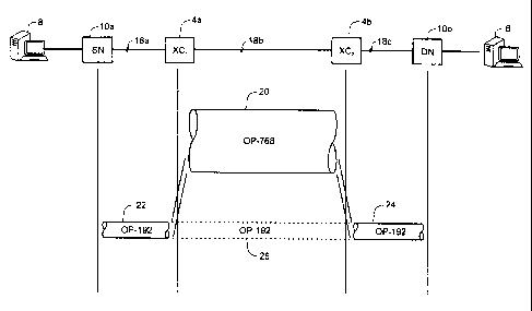
Fig. 2 is a schematic diagram illustrating an
exemplary set-up of the OP-N connection 16 mapped between
the source and destination nodes 10a and 10b. In the
illustrated embodiment, the OP-N connection 16 is an OP-192
CA 02337742 2001-02-22
11997RocA02U 9-13528-102CA
14 -
connection, thus having a bandwidth equivalent to N = 192
STS-1 signals. Within this connection, signal
concatenation is not provisioned, so that an arbitrary
concatenation scheme (up to the bandwidth capacity of the
OP-N) can be defined by an end user. As shown in Fig. 2,
the OP-N connection 16 may be constructed using a layered
model. For example, the network service provider may elect
to set up high bandwidth OP-N core connections between
cross-connects 4 within the core of the network. In the
illustrated example, these high bandwidth core connections
include an OP-768 core connection 20 set up between the
first and second cross-connects 4a and 4b. The
OP-N connection 16 is set up, for example, by a network
service provider in response to a request from an end user
for an end-to-end open connection having a bandwidth of N
192. Setting up this end-to-end open connection requires
that the network service provider establish feeder OP-192
connections 22 and 24 between the source node and the first
cross-connect 4a, and between the second cross-connect 4b
and the destination node 10b. These feeder OP-192
connections 22,24 are then linked by a virtual OP-192
connection 26 which is set up by allocating a portion of
the bandwidth of the OP-768 core connection 20 previously
established between the two cross-connects 4a and 4b.
Throughout the length of the end-to-end
OP-N connection 16, a predetermined number of channels
(i.e. M, an integer) are utilized. Depending on the
traffic mix selected by the end-user, two or more (up to a
limit of M), adjacent parallel channels of the OP-N
connection 16 can be hyper-concatenated to define a hyper-
concatenated connection 27 within the OP-N connection 16.
High bandwidth data traffic originating at the end-user's
communications device 8 is inverse-multiplexed across the
CA 02337742 2001-02-22
11997ROCA02U 9-13528-102CA
15 -
hyper-concatenated channels of the OP-N connection 16, at
the source node 10a, and launched as hyper-concatenated
data streams through the OP-N connection 16. Each channel
carries a respective data stream. Two or more channels may
be either multiplexed within a single waveguide (e.g.
optical fiber) or distributed over two or more waveguides.
At the destination node 10b, the hyper-concatenated data
streams are recombined to recover the original end-user's
data traffic. This inverse-multiplexing and recovery
process is preferably transparent to the end user.
For the purposes of the present invention, the M
channels of the OP-N connection 16 are considered to be
parallel in the sense that although the channels may follow
different paths (e.g. optical fibers), their respective
channel ordering is identical at both the source node 10a
and the destination node 10b. Additionally, the M data
streams are not subject to independent pointer processing
at any intermediate nodes between the source node 10a and
the destination node 10b.
Fig. 3 is a block diagram schematically
illustrating the principal elements of a cross-connect 4 of
the optical network. As shown in Fig. 3, the
cross-connect 4 includes at least one input port 28
connected to a respective upstream fiber 30; a signal
processor 32 for processing respective data streams within
each channel; at least one output port 34 connected to a
respective downstream fiber 36; a switch 38 capable of
providing a signal path for each channel between respective
input and output ports 28, 34; and a controller 40 for
controlling operation of the cross-connect 4. The
controller 40 can be provided with a buffer (not shown) for
temporarily storing information, such as, for example,
CA 02337742 2001-02-22
11997ROCA02U 9-13528-102CA
16 -
routing information for each OP-N routed through the
cross-connect 4.
In the embodiment shown in Fig. 3 the
cross-connect 4 has two input ports 28a and 28b and two
output ports 34a and 34b. However, it will be appreciated
that the cross-connect 4 may be provisioned with a
plurality of ports, of which one or more may be unused. It
will also be appreciated that the ports of the
cross-connect 4 may be configured to handle bi-directional
data traffic. However, in order to simplify the present
description, and aid understanding of the invention, the
embodiment shown in Fig. 3 is provided with unidirectional
ports, two of which (input ports 28a and 28b) are
configured to handle inbound signal traffic, and the other
two (output ports 34a and 34b) are configured to handle
outbound signal traffic.
As shown in Fig. 3, each input port 28 includes a
demultiplexor 42 for demultiplexing the respective channels
of the respective upstream fibers 30a,b. Similarly, each
output port 24 includes a multiplexor 44 for multiplexing
the channels of a respective downstream fiber.
The signal processor 32 and switch fabric 38 are
configured to successively process and route data streams
on a per-channel basis through the cross connect 4. The
signal processor :32 can be designed to process data streams
within an arbitrary number (e.g. P, an integer) of
channels, which will normally be equal to or greater than
the number M of channels of the OP-N connection 16. Because
each OP-N connection mapped through the network is assigned
a unique set of M channels, it is possible for the signal
processor 32 and switch 38 to simultaneously process and
route data streams of two or more OP-N connections routed
CA 02337742 2001-02-22
11997ROCA02U 9-13528-102CA
- 17 -
through the cross-connect 4. It is also possible for the
processor 32 and switch fabric 38 to process and route data
streams on other channels not assigned to an OP-N
connection, in addition to the OP-N traffic. Per-channel
routing of data streams through the switch 38 is known in
the art, and therefore will not be further described.
Per-channel processing of data streams by the signal
processor 32 will be described in greater detail below with
reference to Fig. 4.
Fig. 4 is a block diagram schematically
illustrating the operation and principal elements of the
signal processor 32. In general, the signal processor 32
comprises an array of P channel processors 46, each of
which operates to process a data stream within a respective
one of P channels. Each of the channel processors 46 is
linked (via an interface) in order to exchange strobe
signals which can be used to synchronize adjacent data
streams, in a manner which will be described in greater
detail below. A control unit 48 is provided to control
operations of each of the channel processors 46, and thus
enable synchronization of data streams. Exemplary
operation modes of each channel processor 46 include a
free-run mode, and a slave mode. In the free-run mode,
bits of a data stream are processed through a channel
processor 46 independently of a timing of other data
streams. Conversely, in a slave mode, a data stream is
processed through the channel processor 46 such that the
timing of bits being output from the channel processor 46
is controlled in accordance with a strobe signal received
from an adjacent channel processor. Both of these
exemplary operation modes will be described in greater
detail below with reference to Figs. 5 and 6a - 6b.
CA 02337742 2001-02-22
11997ROCA02U 9-13528-102CA
- 18 -
In general, the number of channel processors 46
provided in the signal processor 32 will equal the number P
of channels handled by the cross-connect 4, and may be
several hundred or more. The channel processors 46 may be
incorporated in a single application specific integrated
circuit (ASIC) or may be distributed across two or more
ASICs connected to operate in parallel. The channel
processors 46 are enabled to operate independently or
cooperatively, as required to handle an arbitrary number of
hyper-concatenated data streams distributed over multiple
channels. In the embodiment illustrated in Fig. 4, the
signal processor 32 includes P channel
processors 46(l)-46(p), of which channel
processors 46(1)-46(M) are assigned to the OP-N
connection 16. Within the OP-N connection 16, a set of
three adjacent channels (CH(1)-CH(3)) form a hyper-
concatenation 27 carrying a corresponding set of
hyper-concatenated data streams that are processed
cooperatively by a corresponding set of three channel
processors 46(1)-46(3). A fourth (independent) data stream
is carried on a respective channel CH(n) and processed by a
corresponding channel processor 46(n).
As mentioned above, any combination of hyper-
concatenated and independent data streams may be processed
in parallel through the signal processor 32. Thus, the
OP-N connection 16 could include two or more
hyper-concatenated connections 27. Furthermore, a
hyper-concatenated connection 27 may, in principle, include
up to P hyper-concatenated data streams, utilizing the
entire capacity of the signal processor 32. Similarly, it
will be appreciated that data streams within multiple OP-N
connections may be processed, in parallel, through the
CA 02337742 2001-02-22
11997ROCA02U 9-13528-102CA
19 _
signal processor 32. Limitations to this degree of
flexibility are as follows:
= within any hyper-concatenation 27, each hyper-
concatenated data stream must be frequency
locked and have the same frame rate (e.g. 8
kilohertz);
= all of the hyper-concatenated data streams
within a hyper-concatenation 27 must be
carried on adjacent parallel channels and must
not have had independent pointer processing at
any node between the source node and the
signal processor 32;
= each hyper-concatenated connection 27 must be
carried on a unique set of channels. The
channels occupied by different
hyper-concatenated connections 27 may be
adjacent one another or may be separated by
one or more channels carrying non-
hyper-concatenated data streams.
As will be described in greater detail below, each
non-hyper-concatenated data stream is processed by the
signal processor 32 by placing the respective channel
processor 46 into a "free run" mode so that the data stream
is processed independently of other data streams. A set of
hyper-concatenated connection 27, on the other hand, is
processed by selecting one channel as a master channel. The
master channel channel processor 46 operates in the free
run mode. This master channel channel processor 46
therefore generates a strobe signal indicative of the
timing of the master data stream. The strobe signal is
propagated from the master channel processor 46 to each of
CA 02337742 2001-02-22
11997ROCA02U 9-13528-102CA
- 20 -
the other channel processors 46 of the hyper-concatenated
connection 27, which are placed in a slave mode dependent
on the received strobe signal. As may be seen in Fig. 4,
the strobe signal 49 can be propagated, channel by channel
in either direction between the channel processors 46.
Consequently, any one of the channels occupied by a
hyper-concatenated connection 27 may be selected as the
master, and the strobe signal propagated as required to the
slave channel processors 46 of the hyper-concatenation 27.
In general, contention between data streams of
different OP-N connections may be avoided by designating a
unique set of channels to each OP-N connection. Similarly,
within each OP-N connection, channel groupings to
accommodate a desired mix of hyper-concatenated and non-
hyper-concatenated data streams can be assigned by the
control unit 48 as required in response to request messages
received from an edge device, which also permits an end
user to alter the traffic mix as required. Normally,
within each group of channels allocated to a particular set
of hyper-concatenated connection 27, the master channel
will be designated by the control unit 48 during set up of
the hyper-concatenation. However, the master channel can
be changed during a communications session in the event of
severely errored frames or loss of frames on the designated
master channel.
Exemplary components and operations of each channel
processor 46 are described below in greater detail with
reference to Figs. 5 and 6a - 6b.
As shown in Fig. 5, a channel processor 46 in
accordance with the present invention generally comprises a
buffer 50, an input timer 52, and an output timer 54. An
interface 56 is also provided to enable the channel
CA 02337742 2001-02-22
11997ROCA02U 9-13528-102CA
- 21 -
processor 46 to send strobe signals to and receive strobe
signals from adjacent channel processors 46.
The buffer 50 provides an elastic store for
temporarily storing bits of a respective data stream. The
buffer 50 is preferably formed as a first-in-first-out
(FIFO) queue having an adjustable read pointer 58. The
FIFO, which may be implemented as a shift register clocked
at a bit rate of the respective data stream, receives
successive bits of the data stream at an input address
(nominally identified as address zero). Stored bits of the
data stream are clocked through the FIFO (from left to
right in the illustrations of Figs. 5, 6a and 6b) When
successive bits arrive at the address identified by the
read pointer 58, they are read out of the FIFO and
transmitted downstream as an outgoing data stream. With
this arrangement, the propagation delay of the data stream
through the buffer 50 is determined by the bit rate, the
length of the buffer 50 (in terms of the number of stored
bits), and the position of the read pointer 58 within the
buffer 50. Synchronizing hyper-concatenated data streams
in concatenation 27 can thus be accomplished by adjusting
respective read pointers 58 within each of the buffers 50
so that a first bit of a frame of each of the
hyper-concatenated data streams is read from the respective
buffer 50 simultaneously, irrespective of when the bits
arrived at the respective buffer 50.
In principle, virtually any amount of misalignment
between hyper-concatenated data streams can be compensated
in this manner. In practice, however, the maximum degree
of misalignment between hyper-concatenated data streams is
limited by the length of the buffers 50. A longer buffer
allows compensation for a greater degree of misalignment.
CA 02337742 2001-02-22
11997ROCA02U 9-13528-102CA
22 -
On the other hand, the use of long buffers increases
equipment cost arid, since the use of buffering within a
channel inevitably imposes transmission delays, the use of
long buffers in each of a series of nodes in an end-to-end
path may result in the accumulation of unacceptable
transmission delay. Additionally, in a case where a degree
of misalignment is equal to or greater than one half a
frame, the frame concatenation sequence becomes ambiguous,
as a determination must be made as to whether a frame is
leading or lagging corresponding frames in other channels
of the concatenation 27. Resolving this ambiguity requires
interpretation of the concatenated frames within each
hyper-concatenated data stream, which is very difficult to
perform at high bit rates. Accordingly, in practice, it is
preferable that the length of each buffer 50 is not more
than about half of the length of a frame. In terms of
transmission delay, a buffer length equivalent to the
number of bits received in a period having a duration of
approximately 250 nano-seconds (nSec) or less is
preferable.
The input timer 52 generates a local strobe signal
indicative of a timing of frames of the incoming data
stream, as well as a clock signal that is phase and
frequency locked with incoming bits of the respective data
stream. The input timer 52 preferably includes a framer
circuit 60 and a clock recovery circuit (not shown) The
framer circuit 60 may include a frame detector (not shown)
which operates in a manner known in the art to detect Al
and A2 bytes of each incoming frame, and a strobe circuit
(not shown) which generates the local strobe signal
frequency locked with a frame rate of the respective data
stream, and phase locked with detection of the Al and A2
bytes of each frame. The local strobe signal is passed to
CA 02337742 2001-02-22
11997ROCA02U 9-13528-102CA
23 -
the output timer 54 for use in controlling a position of
the read pointer 58 for the respective data stream, and
passed to the interfaces 56 for possible transmission to
adjacent channel processors 46. The clock recovery circuit
(not shown) operates to produce clock signals in a manner
well known in the art.
The output timer 54 controls a timing of outgoing
bits of the data stream, by adjusting the location of the
read pointer 58 within the buffer 50. The details of this
operation depend on the operating mode of the channel
processor 46. In particular, in the free running mode, the
output timer 54 controls the timing of outgoing bits of the
respective data stream based principally on the local
strobe signal generated by the input timer 52. In slave
mode, the output timer 54 operates to control the timing of
outgoing bits of the data stream based on both the local
strobe signal and. a master strobe signal received from an
adjacent channel processor 46. Each mode of operation is
accommodated by a phase error detection circuit 64 and a
read pointer adjuster circuit 66.
The phase error detection circuit 64 receives the
local strobe signal as well as a second strobe signal
(described below), and detects a phase difference between
the two strobe signals. This detected phase error is then
used by the read pointer adjustment circuit 66 to apply an
offset to the position of the read pointer 58 in order to
compensate for the detected phase difference. An
additional fixed offset output by an offset register 67
(which may be software provisioned under control of the
control unit 48) may also be supplied to the read pointer
adjustment circuit 66 to compensate for propagation delays
in the various strobe signals, as well as delays incurred
CA 02337742 2001-02-22
11997ROCA02U 9-13528-102CA
24 -
in the phase error detect circuit 64 and the read pointer
adjustment circuit 66.
In an exemplary embodiment, the phase error
detection circuit 64 is implemented as a counter that
operates to count clock pulses between reception of the two
strobe signals. The pulse count value is then passed to
the read pointer adjustment circuit 66 as the detected
phase error. The read pointer adjustment circuit 66 uses
the detected phase error to adjust the read pointer 58 to
an address within the buffer 50 that is offset from a
predetermined base address by a number of bits indicated by
the pulse count.. The optional (software provisioned)
offset output by offset register 67 is also used by the
read pointer adjustment circuit 66 to apply an additional
offset to the read pointer 58. Alternatively, the optional
offset can be used to adjust a position of the base address
relative to an input address of the buffer 50.
In an alternative embodiment (not shown in the
figures), the output timer 54 is implemented by suitable
circuitry and software which operates to measure the phase
difference between the two strobe signals, and calculate an
adjusted position of the read pointer 58 in order to
compensate for the measured phase difference. In this
embodiment, the optional offset output by the offset
register 67 can be omitted, as any additional offsets (e.g.
required to compensate for propagation delays) can be
incorporated into the software implementation of the output
timer 54.
As described above, the phase error detection
circuit 64 determines a phase error between the local
strobe signal and the second strobe signal. The output
timing circuit is operated in the free running mode or the
CA 02337742 2001-02-22
x ~I
11997ROCA02U 9-13528-102CA
25 -
slave mode, as desired, by selecting one of the local
strobe signal and. the master strobe signal as the second
strobe signal. Selection of the second strobe signal is
accomplished by supplying both the local strobe signal and
the master strobe signal to respective inputs of a switch
circuit 68 (e.g. a MUX) which is controlled by a mode
select signal 69 asserted by the control unit 48. Thus in
the free running mode, the switch circuit 68 supplies the
local strobe signal to the phase error detection circuit 64
as the second strobe signal. The phase error detection
circuit 64 calculates a phase difference between the two
sources of the local strobe signal, which yields a zero
phase error. In response to the zero phase error, the read
pointer adjustment circuit 66 sets the position of the read
pointer 58 to correspond with the predetermined base
address, plus any provisioned additional offset. In this
condition, the timing of outgoing bits of the respective
data streams is controlled primarily in accordance with the
local strobe signal. Master strobe signals may be received
from adjacent channel processors 46. However, since these
master strobe signals are not passed to the phase error
detection circuit 68, they do not influence the timing of
outgoing bits of the respective data stream.
Conversely, in the slave mode, the switch
circuit 68 is controlled by the control unit 48 (Fig. 4) to
select a received master strobe signal as the second strobe
signal. In this condition, the phase error detection
circuit 64 operates to determine a phase difference between
the local strobe signal and the master strobe signal, which
generally yields a non-zero value. The read pointer
adjustment circuit then determines a new location for the
read pointer 58 which compensates for the detected phase
difference. Consequently, the timing of outgoing bits of
CA 02337742 2001-02-22
a i
11997ROCA02U 9-13528-102CA
26 -
the respective data stream is controlled in accordance with
the phase difference between the local and master strobe
signals, thereby permitting the data stream to be
synchronized with the master data stream. Interaction
between adjacent channel processors 46 to accomplish this
synchronization will be described in further detail below
with reference to Figs. 6a and 6b.
As discussed above and illustrated in Fig. 5, each
channel processor also includes an interface 56 that sends
and receives strobe signals to and from respective adjacent
channel processors 46. The interface 56 includes a pair of
output circuits 70 and a pair of input circuits 72.
Each input circuit 72 receives a master strobe
signal from a respective adjacent channel processor 46, and
passes the respective master strobe signal to a direction
selector circuit 74. The direction selector circuit 74 is
used to select one of the two master strobe signals, and
the selected signal is passed to the switch circuit 68.
Preferably, the input circuit 72 also performs signal
conditioning on the received master strobe signals.
Exemplary conditioning functions include: re-timing the
master strobe using a local clock (e.g. supplied by the
clock recovery circuit; rising edge detection; and signal
validation (e.g. to ensure that the master strobe signal
has an appropriate predetermined frequency, such as 8 kHz.
This validation process takes into account, and compensates
for, re-timing uncertainty that may result from the master
strobe signal being asynchronously re-timed based on the
locally generated recovered clock signal. A loss of a
strobe signal can also be detected, and used to trigger an
alarm state to the controller unit 48 (Fig. 4).
CA 02337742 2001-02-22
11997ROCA02U 9-13528-102CA
27 -
In an alternative embodiment, the conditioning
functions of the input circuit 72 may be relocated to a
point between the direction selector circuit 74 and the
switch circuit 68, so that a strobe signal can propagate
across multiple channel processors with minimum delay
because signal conditioning is not performed in each
channel processor 46 prior to re-propagation.
The direction selector circuit 74, e.g. a MUX, is
controlled by a direction selection signal 75 asserted by
the control unit 48. The direction selector circuit 74
selects one of the received master strobe signals for use
by the channel processor 46. The selected master strobe
signal, in addition to being passed to the switch
circuit 68, is also passed to the output circuit 70 of each
interface 56 so that (in accordance with the operating mode
of the channel processor 46) the selected master strobe
signal or the local strobe signal can be relayed to each of
the adjacent channel processors 46.
The output circuit 70 of the interface 56 includes
a switch circuit, e.g. a MUX, controlled by the mode select
signal 69 asserted by the control unit 48 (Fig. 4) The
output circuit 70 receives the selected master strobe
signal and the local strobe signal at respective inputs,
and, depending on the asserted state of the mode select
signal, propagates one of the local strobe signal and the
selected master strobe signal to an adjacent channel
processor. When the channel processor 46 is in the free
run mode, the output circuit 70 of the interface 56
propagates the local strobe signal to both adjacent channel
processors. In this mode of operation, the state of the
direction selector circuit 74 is not material, because
neither of the received master strobe signals are utilized.
CA 02337742 2001-02-22
11997ROCA02U 9-13528-102CA
- 28 -
On the other hand, when the channel processor is in a slave
mode, the output circuits 70a,70b propagate the master
strobe signal selected by the direction selector circuit 74
to both of the adjacent channel processors. In this case,
the direction selector circuit 74 is controlled to select
the direction from which a master strobe signal is received
for synchronization purposes.
The process of synchronizing hyper-concatenated
data streams within a hyper-concatenation 27 will now be
described, with reference to the signal processor 32
illustrated in Fig. 4. As shown in Fig. 4, the OP-N
connection 16 includes a hyper-concatenated connection 7
composed of three hyper-concatenated channels CH(1)-CH(3)
carrying respective hyper-concatenated data streams. Each
of the hyper-concatenated data streams is processed by
respective channel processors 46(1)-46(3). Synchronization
of the three hyper-concatenated data streams proceeds as
follows. When the hyper-concatenation 27 is set up, one of
the hyper-concatenated channels (e.g. CH(1)) is designated
as a master channel, and the other hyper-concatenated
channels CH(2) and CH(3) are designated as slave channels.
The corresponding channel processors 46 are likewise
designated as master and slave channel processors. The
master channel processor 46(1) is therefore set to free-run
mode by the control unit 48. Accordingly, the selector
switch 68(1) of the master channel processor 46(1) is set
so that the output timer 54(1) operates exclusively on the
basis of the local strobe signal, and the output
circuits 70a,b of the interface 56(1) are set to pass the
local strobe signal to each adjacent channel processor (in
this example, first slave channel processor 46(2)) as the
master strobe signal. The state of the direction selector
CA 02337742 2001-02-22
11997ROCA02U 9-13528-102CA
- 29 -
circuit 74(1) of the master channel processor 46(1) is
irrelevant.
The slave channel processors 46(2), 46(3) are set
to slave mode by the control unit 48. Thus in each slave
channel processor 46(2), 46(3), the selector switch 68 is
set so that the output timer 54 operates on the basis of
the respective local strobe signal and a received master
strobe signal. The direction selector circuit 74 is set to
select the master strobe signal propagated from the
direction of the master channel processor 46(1). Finally,
each output circuit 70 of the interface 56 is set to
propagate the selected master strobe signal to both
adjacent channel processors.
Accordingly, the first slave channel
processor 46(2), immediately adjacent the master channel
processor 46(1), receives the master strobe signal
propagated from the master channel processor 46(1). This
master strobe signal is selected by the direction selector
circuit 74 and passed to the output timer 54(2). The
master strobe signal is also passed to the output
circuits 70a,b of the interface 56 and thereby passed to
both adjacent channel processors 46(1) and 46(3). The
master strobe signal passed back to the master channel
processor 46(1) is ignored.
The second slave channel processor 46(3) operates
in the same way as the first slave channel processor 46(2).
The direction selector circuit 74(3) is set to select the
master strobe signal propagated from the first slave
channel processor 46(2). The selected master strobe signal
is passed to the output timer 54 and to the output
circuits 70a,b of the interfaces 56. One of the output
circuits 70b passes the master strobe signal back to the
CA 02337742 2001-02-22
11997ROCA02U 9-13528-102CA
- 30 -
first slave channel processor 46(2), where it is ignored.
The other output circuit 70a passes the master strobe
signal to the next adjacent channel processor 46(4) (riot
shown), where, in this example, it is likewise ignored.
In the example described above with reference to
Fig. 4, the local strobe signal generated by the free
running master channel processor 46(1) is propagated as the
selected master strobe signal, to each of the slave channel
processors 46(2) and 46(3) . In fact, the master strobe
signal propagated from the free running master channel
processor 46(1) is propagated (in both directions)
channel-by-channel through the signal processor 32, until
it reaches any of: a channel processor 46 at an edge of the
signal processor 32; another free running (master) channel
processor 46; or a slave channel processor in which the
direction selector circuit 74 is set to select a master
strobe signal received from the opposite direction.
Using the construction and operation of the channel
processors described 46 with reference to Figs. 4 and 5,
any hyper-concatenated data stream in a hyper-concatenated
connection 27 can be designated the master data stream.
However, for reasons that will be explained below in more
detail, a slowest of the hyper-concatenated data streams is
preferably designated as master in order to minimize
trans-channel-processor delay.
In the example shown in Fig. 4, the master channel
CH(1) is at the edge of the signal processor 32, and has
the fastest propagation speed (of the hyper-concatenated
channels). However, any one of channels CH(1), CH(2), or
CH(3) could have been selected as the master, without
affecting the synchronization operation.
CA 02337742 2001-02-22
11997ROCA02U 9-13528-102CA
- 31 -
Figs. 6a and 6b illustrate two examples of channel
processing. In the example illustrated in Fig. 6a, a
hyper-concatenation composed of n hyper-concatenated data
streams distributed over n hyper-concatenated channels are
to be processed by respective channel processors 46 within
the signal processor 32. In this example, the first
arriving signal is assumed to be on channel 1, and the
arrival order of the other data streams follows the channel
order, for the sake of illustration, so that the last
arriving signal is received on channel n. The data stream
on channel 1 is designated as the master. The remaining
channels (CH(2)-CH(n)) are designated as slave channels,
and so synchronize their respective data streams based on a
master strobe signal propagated from channel 1. In
general, the delay period between arrival of the first bits
of the fastest data stream on channel 1, and arrival of the
corresponding last arriving bits of the (slowest) data
stream on channel n is unknown. Accordingly, the base
address used for the read pointer 58 in the master channel
processor is set at a point in the buffer to compensate for
the expected delay for the slowest data stream, plus some
reasonable margin of safety, which may be at or near the
highest address of the master buffer 50. Thus, in the
master channel processor, the read pointer is positioned
near the high address end of the FIFO, so that bits of the
master data stream on channel 1 will transit nearly the
entire length of the respective FIFO before being read to
the outgoing data streamõ By default, the base position of
the read pointers 58 in each of the slave channel
processors is initialized to the same location as in the
master channel processor. When the master channel processor
locks on the first bytes (A1,A2) of an arriving frame, it
generates the master strobe which is propagated across the
CA 02337742 2001-02-22
11997ROCA02U 9-13528-102CA
32 -
hyper-concatenation to each of the slave channel
processors. Each slave channel processor accumulates a
count of a respective clock signal between its local strobe
and receipt of the master strobe signal. The count is then
used to offset the read pointer from the base position.
The read pointers in each of the slave channel processors
on channels 2 through channel n are respectively adjusted
to various positions progressively closer to the input
address for the incoming data stream. Thus, the respective
data streams running in channels 2 through channel n
transit through progressively smaller portions of their
respective FIFOs before being read to the outgoing data
stream and exiting the channel processor. Those data
streams therefore incur correspondingly shorter delay times
within the buffers 50, which effectively advances their
timing with respect to the master data stream, to thereby
synchronize the data streams across all of the associated
channels.
While the example illustrated in Fig. 6a is
effective for use in synchronizing the data streams across
an arbitrary number of hyper-concatenated channels,
designation of the fastest propagating data stream as the
master, in combination with the generally unknown delay of
the slowest propagating data stream, means that the master
data stream may transit almost the entire length of its
buffer, and thereby incur a maximum transmission delay.
Each of the slower data streams experience lesser
transmission delays, but unless the misalignment between
the first arriving bits on channel 1 and corresponding bits
on the slowest channel is equal to the length of the
buffer, then the transmission delays incurred by each data
stream is longer than it needs to be.
CA 02337742 2001-02-22
11997ROCA02U 9-13528-102CA
- 33 -
Clearly, it is desirable to minimize the delay
incurred by each of the data streams. Fig. 6b illustrates
an example in which the number and distribution of data
streams is identical to that of the example shown in
Fig. 6a. Thus the data stream having the highest
propagation speed arrives on channel 1 with the data
streams arriving on channels 2 through n having
progressively slower propagation speeds. However, in this
case the data stream on the slowest channel is designated
as the master, and each of the other channels are
designated as slaves. Because the master data stream is
the last arriving signal, it is not necessary to buffer the
master data stream for any longer than is required to
permit generation of the master strobe signal for use by
the slave channel processors on the other channels. Thus
the read pointer in the master channel processor can be
located at a base address that is at or very near the input
address (zero), so that little if any of the buffer within
the master channel processor is utilized. In each of the
slave channel processors, the respective read pointers are
initialized to a base address near the input address of the
buffer by default, and are adjusted to positions
progressively further away from the input address in
accordance with the time delay between arrival of bits on
the respective slave channel and detection of the master
strobe indicating the arrival of corresponding bits on the
master channel. As can be seen in Fig. 6b, this results in
each data stream incurring a minimal delay while
synchronization of the hyper-concatenated data streams
across all of the hyper-concatenated channels is achieved.
Although the invention has been explained with
reference to optical networks and fiber links, it will be
understood by those skilled in the art that the principles
CA 02337742 2001-02-22
11997ROCA02U 9-13528-102CA
- 34 -
and components of the invention may also be applied to the
transmission of data over two or more wireless data
channels using a wireless device, such as a Code Division
Multiplex Process (CDMA) wireless transceiver.
The embodiment(s) of the invention described above
is(are) intended to be exemplary only. The scope of the
invention is therefore intended to be limited solely by the
scope of the appended claims.