Language selection

Search

Patent 2337874 Summary

Third-party information liability

Some of the information on this Web page has been provided by external sources. The Government of Canada is not responsible for the accuracy, reliability or currency of the information supplied by external sources. Users wishing to rely upon this information should consult directly with the source of the information. Content provided by external sources is not subject to official languages, privacy and accessibility requirements.

Claims and Abstract availability

Any discrepancies in the text and image of the Claims and Abstract are due to differing posting times. Text of the Claims and Abstract are posted:

  • At the time the application is open to public inspection;
  • At the time of issue of the patent (grant).
(12) Patent Application: (11) CA 2337874
(54) English Title: A SWITCHABLE INDUCTOR
(54) French Title: INDUCTEUR COMMUTABLE
Status: Deemed Abandoned and Beyond the Period of Reinstatement - Pending Response to Notice of Disregarded Communication
Bibliographic Data
(51) International Patent Classification (IPC):
  • H01P 3/08 (2006.01)
(72) Inventors :
  • ZHOU, SHU-ANG (Sweden)
  • WIKBORG, ERLAND (Sweden)
(73) Owners :
  • TELEFONAKTIEBOLAGET LM ERICSSON
(71) Applicants :
  • TELEFONAKTIEBOLAGET LM ERICSSON (Sweden)
(74) Agent: MARKS & CLERK
(74) Associate agent:
(45) Issued:
(86) PCT Filing Date: 1999-07-16
(87) Open to Public Inspection: 2000-01-27
Availability of licence: N/A
Dedicated to the Public: N/A
(25) Language of filing: English

Patent Cooperation Treaty (PCT): Yes
(86) PCT Filing Number: PCT/SE1999/001283
(87) International Publication Number: WO 2000004603
(85) National Entry: 2001-01-16

(30) Application Priority Data:
Application No. Country/Territory Date
9802583-6 (Sweden) 1998-07-17

Abstracts

English Abstract


An inductor for microwave frequencies has a substantially planar structure and
is constructed of a transmission line designed as a linear microstrip element
made of a central line (5) comprising normal electrically conducting material,
such as a suitable metal. The microstrip element has a width which is varied
by making areas (7) at sides of the central line (5) superconducting. In
changing the effective width of the microstrip the inductance thereof is
changed accordingly. The areas at the sides of the microstrip element are
located directly at the central, normal metal conductor. These areas have in
the non-superconducting state some electrical conductivity which can be rather
low but owing to the fact that they contact the normal central metal conductor
only at a very narrow edge instead of contacting it at a large surface they do
not significantly affect the transmission characteristics of the transmission
path when the superconducting areas (7) are in their normal state.


French Abstract

L'invention concerne un inducteur pour hyperfréquences, de structure sensiblement plane, constitué d'une ligne de transmission conçue sous la forme d'un élément microbande linéaire comportant une ligne (5) centrale comprenant un matériau électroconducteur normal, par exemple un métal approprié. La largeur de l'élément microbande peut être modifiée en rendant les zones (7) de part et d'autre de la ligne (5) centrale supraconductrices. La modification de la largeur effective de la microbande permet de modifier en conséquence l'induction de ladite microbande. Les zones de part et d'autre de l'élément microbande se situent directement u niveau du conducteur métallique central. Ces zones possèdent, à l'état non supraconducteur, une certaine conductivité électrique, qui peut être plutôt faible mais qui, du fait qu'elles ne sont au contact du conducteur métallique normal qu'au niveau d'une arête très étroite et non au niveau d'une large surface, n'ont qu'une faible incidence sur les caractéristiques de transmission du chemin de transmission, lorsque les zones supraconductrices se trouvent dans leur état normal.

Claims

Note: Claims are shown in the official language in which they were submitted.

4
CLAIMS
1. An inductor for microwaves, characterized by a central- microstrip line
made of an
electrically conducting material exhibiting no superconducting properties
above a considered
temperature and regions made of a material exhibiting superconducting
properties above the
considered temperature, the regions being located at sides of the central
microstrip line and in
the same plane as the central microstrip line.
2. An inductor according to claim 1, characterized in that the central
microstrip line
has a shape of a strip of a uniform width.
3. An inductor according to any of claims 1 - 2, characterized in that the
regions have
shapes of strips of uniform widths.
4. An inductor according to claim 3, characterized in that all the regions
have the same
uniform width.
5. An inductor according to any of claims 1 - 4, characterized by control
means for
making an electrical current flow through the inductor, thereby bringing, when
the inductor is
above the considered temperature and the regions are in a superconducting
state, the regions
to change to a non-superconducting state.

Description

Note: Descriptions are shown in the official language in which they were submitted.


CA 02337874 2001-O1-16
WO 00104603 PCT/SE99/0~283
1
A SWITCHABLE INDUCTOR
TECHNICAL FIELD
The present invention relates to an inductor to be used in microwave
integrated circuits,
in particular an inductor being formed by a microstrip line.
s BACKGROUND OF THE INVENTION AND STATE OF THE ART
In transmission paths in microwave integrated circuits there is of course a
need for
various components such as inductors like in other electronic fields. In
particular there may
be a need for an inductor, the characteristics of which can be varied, such as
an inductor
which can be switched between two inductance values as controlled by an
electrical signal.
,o In Japanese patent application JP 2/101801 a microwave band-rejection
filter is
disclosed having transmission lines designed as linear microstrip, metal
elements placed on
top of an area of a layer of the superconducting material. The superconducting
material area
has a pattern substantially agreeing with that of the metal conductor except
in some regions
where the width of the superconducting area is larger than that of the metal
conductor. When
,s the superconducting material is made to pass into a non-superconducting
state, most of the
electric current passes through the common metal material of the metal
conductor whereas, in
the superconducting state, the electrical current passes only through the
superconducting
underlying material. The elements thereby obtain a variable filtering effect.
However, a
disadvantage of this design resides in providing a region having some, though
it may be low,
Zo electrical conductivity placed under the normal conductor, since this
region causes losses in
the transmission line. The conductivity of materials, which are
superconducting at a low
temperature and are suitable for microwave integrated circuits, have in their
normal state an
electrical conductivity corresponding to some 10-3 to 10-2 of the electrical
conductivity of the
material of the always normal metal conductor.
is SUMMARY
It is an object of the invention to provide an electrical inductor of the
microstrip type
for microwaves exhibiting low losses.
Thus, an inductor for primarily microwave frequencies is constructed of a
transmission
line designed as a linear microstrip element made of a central line comprising
normal
3o electrically conducting material, such as a suitable metal. The microstrip
element has a width
which is varied by making areas at the sides of the central line
superconducting. In changing
the effective width of the microstrip the inductance thereof is changed
accordingly. The areas
at the sides of the microstrip element are located directly at the central,
normal metal
conductor and are thus electrically connected thereto along at least portions
of the sides or of
3s the edges of the central, normal metal conductor. These areas have in their
non-
superconducting state some electrical conductivity which can be rather low but
owing to the
fact that they contact the normal central metal conductor only at a very low,
thin or narrow
edge instead of contacting it at a large surface they do not significantly
affect the transmission
characteristics of the transmission path when the superconducting areas are in
their normal,

CA 02337874 2001-O1-16
WO 00/04603 PCT/SE99/01283 _
2
not superconducting state.
BRIEF DESCRIPTION OF THE DRAWINGS
The invention will now be described by way of a non-limiting embodiment with
reference to the accompanying drawings, in which:
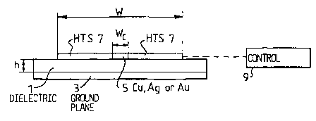
s Fig. 1 is a cross-sectional view of a planar, switchable microwave inductor,
Fig. 2a is a cross-sectional view identical to that of Fig. 1 illustrating
electrical current
distribution when some regions are in a superconducting state,
Fig. 2b is a cross-sectional view similar to that of Fig. 2a illustrating
electrical current
distribution when some regions have changed from a superconducting state to a
normal state,
,o and
Fig. 3 is a diagram of the inductance of an inductor as a function of time
illustrating the
case where some regions of an inductor change from a superconducting state to
a normal
state.
DETAILED DESCRIPTION
,s In the cross-sectional view of Fig. 1 an inductor having a variable
inductance intended
to be connected in e.g. a microwave circuit is illustrated. The inductor is
built on a dielectric
substrate 1 having an electrically conducting ground layer 3, such as a metal
layer of e.g. Cu,
Ag or Au, on its bottom surface, the ground layer covering substantially all
of the bottom
surface as a contiguous layer. On the top surface there is a patterned
electrically conducting
20 layer 5 having a high electrical conductivity, -such as a suitable metal,
e.g. of the same metal
as the bottom layer, i. e. of copper, silver or gold. The patterned layer 5
has the shape of
strip of uniform width W~ and forms a transmission or propagation path for
microwaves. The
strip 5 has electrically conducting areas or regions 7 located directly at the
side or sides of
the conductor strip 5. These regions 7 are made of a potentially
superconducting material,
is preferably a high temperature superconducting material. The regions 7
comprise strips located
at both sides of the central metallic strip 5, preferably symmetrically in
relation thereto, these
strips thus having the same uniform width as each other. The width of the
superconducting
strips together with the central conductor is denoted by W.
In the normal state of the potentially superconducting regions 7 they have,
for typical
ao high temperature superconductivity materials, an electrical conductivity Qn
of about 5105 S/m
to be compared to the electrical conductivity Q~ of the central metal
conductor 5 comprising
about 108 S/m. In the case where the potentially superconducting regions 7 are
in a normal
state, the electrical current will accordingly flow almost entirely in the
central conductor 5.
The current distribution for this non-superconducting state appears from the
diagram of Fig.
as 2b. The current distribution is here substantially uniform over the width
W~ of the conductor
5.
In the other case where the regions 7 are in a superconducting state, alI of
the electrical
current will only pass in the lateral superconducting areas 7 and at the outer
edges thereof,
see the current distribution diagram of Fig. 2a, according to the Meissner
effect.

CA 02337874 2001-O1-16
WO 00/04603 PCT/SE99/01283
3
The inductance of a microstrip line is mainly determined by the total width w
of the
line, e.g. being approximately inversely proportional to the width, i.e.
approximately
proportional to 1/w, provided that the height h of the microstrip line to its
ground plane 3 is
fixed. Thus, changing the state of the potentially superconducting regions 7
to enter and to
s leave the superconducting state wilt change the inductance of the microstrip
Iine as described
hereinabove, the inductance then adopting a lower and a higher value
respectively, see the
diagram of Fig. 3.
A switching between the superconducting state and the normal state of the
potentially
superconducdng regions 7 can be achieved in any conventional way, such as by
varying the
,o temperature, by varying the magnetic field or by varying a direct current
level as to what is
required or desired. This switching is symbolized by the control unit 9 shown
in Fig. 1. A
preferred way may be to have the control unit make an electrical current
higher than the
critical current of the superconducting material pass or not pass through the
microstrip line.
By letting always a fixed bias current, a direct current, pass through the
line, the fixed bias
,s current having an intensity slightly slower than that of the critical
current, and adding or not
adding thereto a small control current such as a current pulse, the reversible
switching
between the superconducting state and the normal state can be made extremely
fast. The
general appearance of the switching operation appears from the diagram of Fig.
3. Here, first
the regions 7 of the microstrip line are in a superconducting state, the
microstrip line have a
zo first low inductance Lsuper and then the state is changed to normal,
producing a change of the
inductance to a higher value Lnor~~t. Then there is a small transition time r
before the change
of inductance is actually effected, for instance when the current through the
microstrip line is
suddenly increased.
Numerical simulation has indicated that the inductance L of a microstrip line
can be
zs easily increased to its double value for a suitable width of the
superconducting regions 7,
working at microwave frequencies.

Representative Drawing
A single figure which represents the drawing illustrating the invention.
Administrative Status

2024-08-01:As part of the Next Generation Patents (NGP) transition, the Canadian Patents Database (CPD) now contains a more detailed Event History, which replicates the Event Log of our new back-office solution.

Please note that "Inactive:" events refers to events no longer in use in our new back-office solution.

For a clearer understanding of the status of the application/patent presented on this page, the site Disclaimer , as well as the definitions for Patent , Event History , Maintenance Fee  and Payment History  should be consulted.

Event History

Description Date
Inactive: IPC expired 2023-01-01
Application Not Reinstated by Deadline 2004-07-16
Time Limit for Reversal Expired 2004-07-16
Deemed Abandoned - Failure to Respond to Maintenance Fee Notice 2003-07-16
Letter Sent 2002-02-19
Inactive: Single transfer 2002-01-14
Inactive: Cover page published 2001-05-01
Inactive: First IPC assigned 2001-04-25
Inactive: Courtesy letter - Evidence 2001-04-03
Inactive: Notice - National entry - No RFE 2001-03-28
Application Received - PCT 2001-03-24
Application Published (Open to Public Inspection) 2000-01-27

Abandonment History

Abandonment Date Reason Reinstatement Date
2003-07-16

Maintenance Fee

The last payment was received on 2002-07-16

Note : If the full payment has not been received on or before the date indicated, a further fee may be required which may be one of the following

  • the reinstatement fee;
  • the late payment fee; or
  • additional fee to reverse deemed expiry.

Please refer to the CIPO Patent Fees web page to see all current fee amounts.

Fee History

Fee Type Anniversary Year Due Date Paid Date
MF (application, 2nd anniv.) - standard 02 2001-07-16 2001-01-16
Basic national fee - standard 2001-01-16
Registration of a document 2002-01-14
MF (application, 3rd anniv.) - standard 03 2002-07-16 2002-07-16
Owners on Record

Note: Records showing the ownership history in alphabetical order.

Current Owners on Record
TELEFONAKTIEBOLAGET LM ERICSSON
Past Owners on Record
ERLAND WIKBORG
SHU-ANG ZHOU
Past Owners that do not appear in the "Owners on Record" listing will appear in other documentation within the application.
Documents

To view selected files, please enter reCAPTCHA code :


To view images, click a link in the Document Description column. To download the documents, select one or more checkboxes in the first column and then click the "Download Selected in PDF format (Zip Archive)" or the "Download Selected as Single PDF" button.

List of published and non-published patent-specific documents on the CPD .

If you have any difficulty accessing content, you can call the Client Service Centre at 1-866-997-1936 or send them an e-mail at CIPO Client Service Centre.


Document
Description 
Date
(yyyy-mm-dd) 
Number of pages   Size of Image (KB) 
Representative drawing 2001-05-01 1 5
Description 2001-01-16 3 206
Abstract 2001-01-16 1 55
Drawings 2001-01-16 1 19
Claims 2001-01-16 1 29
Cover Page 2001-05-01 1 36
Notice of National Entry 2001-03-28 1 193
Request for evidence or missing transfer 2002-01-17 1 108
Courtesy - Certificate of registration (related document(s)) 2002-02-19 1 113
Courtesy - Abandonment Letter (Maintenance Fee) 2003-08-13 1 176
Reminder - Request for Examination 2004-03-17 1 116
Correspondence 2001-03-28 1 23
PCT 2001-01-16 8 306