Note: Descriptions are shown in the official language in which they were submitted.
CA 02339062 2008-08-12
LOW CAPACITANCE SURGE PROTECTOR
FOR HIGH SPEED DATA TRANSMISSION
BACKGROUND OF THE INVENTION
Field of the Invention
This invention relates to methods and apparatus for suppressing transient
voltages and current spikes on high speed transmission lines for the purpose
of
protecting electronic equipment.
Description of the Prior Art
Prior art systems for protecting electrical equipment from the damaging
effects
of voltage transients and current spikes associated with energy surges are
well known.
Such systems have included the use of gas dissipating tubes, semiconductor
devices,
or some combination thereof.
Gas dissipating tubes, or spark gaps, dissipate energy by producing an
electrical arcing to ground. This arcing occurs through the ionization of a
gas of
known dielectric strength during an electrical surge condition.
While gas dissipating tubes provide sufficient suppression for most energy
surges, their relatively slow response time results in a failure to suppress
fast rise time
voltage transients and current spikes. Such transients and spikes are capable
of
destroying electrical equipment connected to the electrical line upon which
the
voltage transients and current spikes are induced.
1
CA 02339062 2000-11-23
WO 99/62158 PCT/US99/11957
Figure 1 shows a conventional surge protector which employs a gas
dissipating tube 2 connected between two electrical transmission lines 4, 6,
which
lines carry signals to electronic equipment, such as computer or telephony
equipment,
connected thereto. In telephone systems, transmission lines 4, 6 may be a tip
and ring
line, respectively.
Figure 3 is a graph of voltage from one electrical line 4, 6 to ground versus
time after a first pulse is introduced to one electrical line 4, 6 of the
circuit in Figure 1.
The first pulse ramps up to its maximum voltage of 5kV (kilovolts) in 10 s
(microseconds) and decays to one-half the maximum voltage in 700gs. This first
pulse
will be referred to as a 10/700 pulse.
As the first pulse ramps up, the voltage across the gas tube increases. As a
result, the gas tube begins to charge. When the gas tube is fully charged, the
gas in the
gas tube will ionize and the pulse will be dissipated. In Figure 3, the gas is
shown to
have ionized at 298V. The ionization occurred 2.6ias after the pulse was
introduced.
Figure 4 is a graph of voltage from one electrical line 4, 6 to ground versus
time after a second pulse was introduced to one electrical line 4, 6 of the
circuit in
Figure 1. The second pulse ramps up to its maximum voltage of 4kV in 5ns
(nanoseconds) and decays to one-half the maximum voltage in 50ns. This second
pulse will be referred to as a 5/50 pulse.
The circuit operates in the same manner as when the 10/700 pulse was
introduced. Since the 5/50 pulse has a faster rise time than the 10/700 pulse,
however,
the voltage spikes up to 2.96kV before the gas in the gas tube ionizes.
Moreover,
after firing, the gas tube does not clamp the voltage low enough to protect
the
electronic equipment. The voltage rises to above :l kV several times during
the
duration of the 5/50 pulse and only begins to drop off after the pulse has
finished.
2
CA 02339062 2000-11-23
WO 99/62158 PCT/US99/11957
The response time of semiconductor-type surge suppressors is faster than that
of gas dissipating tubes. The typical avalanche semiconductor device used,
however,
is limited in the level of energy which it can dissipate before being
destroyed by the
electrical surge. Further, these devices add significant levels of capacitance
to the
surge protection circuit. Typical gas tubes have capacitances of between about
2pF
(picofarads) and about 7pF. The semiconductor circuits used in conjunction
with the
gas tubes, however, increase the capacitance of the conventional surge
protector
circuit to about 100pF. The problem with such relatively high capacitance is
that it
limits the bandwidth and, therefore, the signal transmission rate of the
transmission
line to which the surge protector is connected.
Examples of such prior art designs include arrangements of gas dissipating
tubes in combination with Zener diodes or some other semiconductor device with
similar clamping characteristics. Typically, these circuits include additional
elements
which introduce added capacitance or inductance to the circuit.
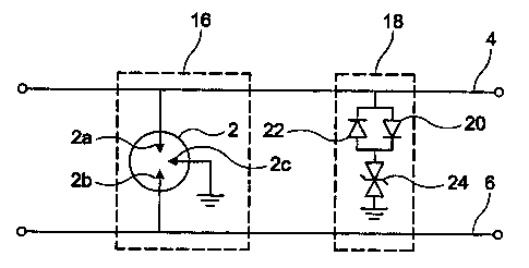
Another conventional surge protector is shown in Figure 2. It includes a gas
dissipating tube 2 connected across electrical lines 4, 6 and two avalanche
semiconductors. One avalanche semiconductor 8 is connected between electrical
line
4 and ground and the other avalanche semiconductor 10 is connected between
electrical line 6 and ground.
Figure 5 is a graph of voltage from one electrical line 4, 6 to ground versus
time after a 10/700 pulse is introduced to one electrical line 4, 6 of the
circuit in
Figure 2.
As the 10/700 pulse ramps up, the voltage across the gas tube increases. As a
result, the gas tube begins to charge. When the voltage across the gas tube
reaches the
breakdown voltage of the avalanche semiconductor, the avalanche semiconductor
sinks current and clamps the voltage across the gas tube at the avalanche
3
CA 02339062 2000-11-23
WO 99/62158 PCT/US99/11957
semiconductor's breakdown voltage, thereby, protecting the attached electronic
equipment.
In Figure 5, the avalanche semiconductor began sinking current when the
voltage across the gas tube reached 222V. The 222V level was reached 2 s after
the
10/700 pulse was introduced to the electrical line. The voltage across the gas
tube is
then clamped at 222V by the avalanche semiconductor. After the avalanche
semiconductor clamps the voltage, the gas tube will continue to charge until
the gas in
the gas tube ionizes and dissipates the pulse. Figure 5 shows the gas ionized
3.2 s
after the pulse was introduced on the line.
Figure 6 is a graph of voltage from one electrical line 4, 6 to ground versus
time after a 5/50 pulse is introduced to either electrical line 4, 6 of the
circuit in Figure
2. The circuit operates in the same manner as when the 10/700 pulse was
introduced.
The faster rise time of the 5/50 pulse, however, results in a voltage spike of
360V
before the avalanche semiconductor begins clamping the voltage. Once the
avalanche
semiconductor starts to sink current and clamp the voltage, the voltage drops
to less
than 250V within 22ns of the pulse being introduced to the line.
A further example of a surge protector is disclosed in United States Patent
No.
4,683,514 to Cook. The Cook patent discloses the use of a spark gap disposed
across
an electrical line and in parallel with an avalanche semiconductor device. An
energy
surge induced on the electrical line will cause the semiconductor circuit to
clamp the
transient at the breakdown voltage of the semiconductor device and will cause
the
spark gap to fire within a specified time period. The addition of the
avalanche
semiconductor device adds a significant capacitance to the electrical line,
thus
degrading higher frequency signals carried by the line.
4
CA 02339062 2000-11-23
WO 99/62158 PCT/US99/11957
OBJECTS AND SUMMARY OF' THE INVENTION
It is an object of the present invention to provide an improved electrical
line
surge protector which can be used to protect electronic equipment from energy
surges
including normal and fast rise time voltage transients and current spikes
induced by
lightning and electromagnetic pulses without loading down the circuit with
increased
capacitance.
It is a further object of the present invention to provide a surge protector
with
nearly identical levels of capacitance from line-to-line and line-to-ground in
a
balanced circuit arrangement.
It is an even further object of the present invention to provide a method of
reducing the capacitance of a surge protector to enable electronic equipment
to be
protected and at the same time allow high speed data transmission.
The low capacitance surge protector is comprised of a gas tube, a first
avalanche semiconductor, and at least a first parallel arrangement of diodes
connected
in series with the first avalanche semiconductor. The at least first parallel
arrangement
of diodes and first avalanche semiconductor forming a first series arrangement
of
components. The first series arrangement is connected between a first
conductor (e.g.,
a tip line in a telephone system) and ground. The at least first parallel
arrangement of
diodes includes at least one pair of diodes. The diodes of the at least one
pair of diodes
are coupled together in opposite polarity.
A second embodiment includes at least a second parallel arrangement of
diodes (connected in opposite polarity to each other) connected in series with
a second
avalanche semiconductor. The at least second parallel arrangement of diodes
and
second avalanche semiconductor forming a second series arrangement of
components.
The second series arrangement of componenets is connected between ground and a
second conductor (e.g., a ring line in a telephone system).
5
CA 02339062 2000-11-23
WO 99/62158 PCTIUS99/11957
The parallel arrangements of diodes are placed in series with the avalanche
semiconductors to effectively reduce the overall capacitance of the surge
protector
measured from line-to-line or from line-to-ground.
In a third embodiment each one of the first series arrangement of components
and second series arrangement of components includes two parallel arrangements
of
diodes (the diodes in each parallel arrangement being connected in opposite
polarity)
in series with each of the avalanche semiconductors. The additional parallel
arrangments of diodes further reduce the capacitance of the surge protector
from line-
to-line and line-to-ground.
In a preferred embodiment, a three element gas tube includes a first element,
a
second element, and a ground element. The first element is connected to the
line 4,
the second element is connected to the line 6, and the ground element is
connected to
ground. A first pair of diodes which are interconnected in series cathode to
cathode
are connected between the line 4 and the line 6. A second pair of diodes which
are
interconnected in series anode to anode are connected between the line 4 and
the line
6. The interconnected cathodes of the first series arrangement of diodes is
connected
to one end of a first avalanche semiconductor, whose other end is connected to
the
anode of a fifth diode. The cathode of the fifth diode is grounded.
Alternatively, the
interconnected cathodes may be connected to the anode of the fifth diode,
whose
cathode is connected to one end of the first avalanche semiconductor, which in
this
case, the second end of the first avalanche semiconductor is grounded. The
interconnected anodes of the second series arrangement of diodes is connected
to one
end of a second avalanche semiconductor, whose other end is connected to the
cathode of a sixth diode. The anode of the sixth diode is grounded.
Alternatively, the
interconnected anodes may be connected to the cathode of the sixth diode,
whose
anode is connected to one end of the second avalanche semiconductor, which in
this
case, the second end of the second avalanche semiconductor is grounded.
6
CA 02339062 2000-11-23
WO 99/62158 PCT/US99/11957
The present invention also includes a method of reducing the capacitance of a
surge protector circuit having a gas discharge tube and an avalanche
semiconductor
coupled in parallel with the gas discharge tube. The gas discharge tube and
avalanche
semiconductor are electrically coupled between an. electrical line and ground.
The
avalanche semiconductor is electrically connected in series with at least one
parallel
arrangement of diodes. Each parallel arrangement of diodes includes a pair of
diodes
which are coupled in opposite polarity to each other. The pair of diodes have
a total
capacitance associated therewith. The avalanche semiconductor also has a
capacitance
associated therewith. The parallel arrangement of diodes and the avalanche
semiconductor are electrically coupled in series which causes the total
capacitance of
the parallel arrangement of diodes and capacitance of the avalanche
semiconductor to
combine in series. The result is a reduced total capacitance of the surge
protector
between the electrical line and ground. Preferably, each of the diodes of the
pair of
diodes in the method of reducing the capacitance of a protection circuit are
fast
recovery diodes. A similar arrangement of diodes and an avalanche
semiconductor
can be coupled between a second electrical line and ground to reduce the
capacitance
of the protection circuit between the second electrical line and ground.
These and other objects, features, and advantages of the present invention
will
be apparent from the following detailed description of illustrative
embodiments
thereof, which are to be read in connection with the accompanying drawings.
BRIEF DESCRIPTION OF THE DRAWINGS
Figure 1 is a schematic diagram of a prior art surge protector circuit which
consists of a gas tube.
Figure 2 is a schematic diagram of a prior art surge protector which consists
of
a combination of a gas tube and an avalanche semiconductor.
7
CA 02339062 2000-11-23
WO 99/62158 PCT/US99/11957
Figure 3 is a graph of voltage versus time illustrating the voltage across the
gas dissipating tube in the circuit of Figure 1 after a 10/700 pulse is
introduced onto
either electrical line.
Figure 4 is a graph of voltage versus time illustrating the voltage across the
gas dissipating tube in the circuit of Figure 1 after a 5/50 pulse is
introduced onto
either electrical line.
Figure 5 is a graph of voltage versus time illustrating the voltage across the
gas dissipating tube in the circuit of Figure 2 after a 10/700 pulse is
introduced onto
either electrical line.
Figure 6 is a graph of voltage versus time illustrating the voltage across the
gas dissipating tube in the circuit of Figure 2 after a 5/50 pulse is
introduced onto
either electrical line.
Figure 7 is a functional block diagram of a surge protector formed in
accordance with the present invention.
Figure 8 is a functional block diagram of a surge protector formed in
accordance with the present invention which illustrates the internal blocks of
a surge
protector.
Figure 9 is a schematic diagram of one embodiment of a surge protector
formed in accordance with the present invention.
Figure 10 is a schematic diagram of a second embodiment of a surge protector
formed in accordance with the present invention.
Figure 11 is a schematic diagram of a third embodiment of a surge protector
formed in accordance with the present invention.
8
CA 02339062 2000-11-23
WO 99/62158 PCTIUS99/11957
Figure 12 is a schematic diagram of a fourth embodiment of a surge protector
formed in accordance with the present invention.
Figure 13 is a graph of voltage versus time illustrating the voltage across
the
gas dissipating tube in the circuit of Figure 10 after a 10/700 pulse is
introduced onto
either electrical line.
Figure 14 is a graph of voltage versus time illustrating the voltage across
the
gas dissipating tube in the circuit of Figure 10 after a 5/50 pulse is
introduced onto
either electrical line.
Figure 15 is a graph of voltage versus time illustrating the voltage across
the
gas tube in Figure 11 after a 10/700 pulse is introduced onto either
electrical line.
Figure 16 is a graph of voltage versus time illustrating the voltage across
the
gas tube in Figure 11 after a 5/50 pulse is introduced onto either electrical
line.
Figure 17 is a graph of voltage versus time illustrating the voltage across
the
gas tube in Figure 12 after a 10/700 pulse is introduced onto either
electrical line.
Figure 18 is a graph of voltage versus time illustrating the voltage across
the
gas tube in Figure 12 after a 5/50 pulse is introduced onto either electrical
line.
Figure 19 is a graph of signal loss in dB versus frequency illustrating the
signal loss after installing the surge protector circuit.
9
CA 02339062 2000-11-23
WO 99/62158 PCT/US99/11957
DETAILED DESCRIPTION OF THE PREFERRED EMBODIMENTS
Referring initially to Figure 7, a block diagram of a surge protector is shown
illustrating the functional relationship of the protector's various
components.
Electrical lines 4, 6 may be any type of electrical line to which electronic
equipment
may be connected, for example, a telephone system's tip or ring line. In a
preferred
embodiment, the surge protector 12 is connected across a telephone line
including a
tip line and/or a ring line. A more detailed block diagram of the surge
protection
system is shown in Figure 8.
As shown in Figure 8, the surge protector 1.2 comprises a clamping circuit 18
and an energy dissipating means 16. Electronic equipment 14 is the equipment
connected to the electrical line which the invention serves to protect from
energy
surges. Electronic equipment 14 may be any type of electronic equipment,
including
telecommunications electronics, computers, or instrumentation. The
functionality of
these individual system components will now be described in the context of a
specific
embodiment of the present invention.
A specific embodiment of a surge protector formed in accordance with the
present invention is illustrated in the schematic diagram of Figure 9. It is
to be
understood that electrical line 4, 6 in a preferred embodiment may either be a
telephone tip line or ring line. The dissipating means 16 described previously
in
connection with the block diagram of Figure 8 may include a gas dissipating
tube 2.
Gas dissipating tube 2 includes a first electrode 2a connected to one
electrical line 4,
6, a second electrode 2b connected to the other electrical line 4, 6, and a
third
electrode 2c connected to ground. Ground may be a ground line or a ground tie
point.
The clamping circuit 18 described previously in connection with the block
diagram of Figure 8 is shown in the embodiment of Figure 9 as including a pair
of low
capacitance, fast recovery diodes 20, 22 which are connected in parallel and
in
opposite polarity to each other. The parallel arrangement of diodes 20, 22 is
CA 02339062 2000-11-23
WO 99/62158 PCT/US99/11957
connected to one of electrical lines 4 or 6. The clamping circuit 18 further
includes a
bidirectional avalanche semiconductor 24, such as a TVS, which is connected
between
the parallel arrangement of diodes 20, 22 and ground.
The surge protection system suppresses energy on electrical line 4, 6 in the
following manner. Assume an energy surge occurs on electrical line 4 or 6. The
source of the surge may be either lightning or an electromagnetic pulse,
inducing
normal or fast rise time voltage transients or current spikes on the line. The
surge
may be on the order of a 4kV (kilovolt) fast transient burst pulse with a
5/50ns
(nanosecond) waveshape (i.e., the pulse will ramp up to its maximum voltage of
4kV
in Sns and decay to one-half its peak voltage in 50ns). The surge may also
have an
impulse discharge current of 5kA (kiloampere) with an 8/20 s (microsecond)
waveshape (i.e., the pulse will ramp up to its maximum current of 5kA in 8/Zs
and
decay to one-half its peak current in 20 s). It is to be appreciated that
these surge
characteristics are not intended to be maximum suppression limits of the surge
protector; rather, they are merely illustrative of the magnitude of the surge
that the
system is ordinarily capable of handling.
As the voltage of the transient pulse begins to increase, the avalanche
semiconductor 24 will reach its breakdown voltage, causing the transient to be
clamped at the breakdown voltage within nanoseconds. The breakdown voltage
will
be at a safe level for the attached electronic equipment 14. The slower gas
tube 2 will
then have time to react to the pulse and discharge the transient before the
elements of
the clamping circuit 18 or electrical equipment 14 are damaged. The purpose of
connecting the parallel arrangement of diodes 20, 22 in series with avalanche
semiconductor 24 is to reduce the overall capacitance of the surge protector
between
the electrical lines 4, 6 and ground, yet still provide the electronic
equipment
connected to the electrical lines 4, 6 with surge protection which includes
the high
current shunting capability of the gas discharge tube 2 and the fast reaction
time to
transients afforded by the avalanche semiconductor 24.
11
CA 02339062 2000-11-23
WO 99/62158 PCT/US99/11957
The parallel capacitance of diodes 20, 22 sum in series with the capacitance
of
the avalanche semiconductor 24 in accordance with the equation:
CP x CA
CT = Eg.
CP+CA
where CT is the capacitance of the clamping circuit 18 between the electrical
lines 4, 6
and ground, CP is the capacitance of the parallel arrangement of diodes 20,
22, and CA
is the capacitance of avalanche semiconductor 24.
A preferred circuit, as shown in Figure 9, uses as a gas discharge tube 2,
Part
No. T22-C200X manufactured by Siemens Components, Inc. of Iselin, New Jersey,
having an approximate capacitance of 2-5pF; as diodes 20, 22, Part No. 50-400-
40
manufactured by Sussex Semiconductor of Fort Meyers, Florida, each having a
capacitance of approximately 10-15pF; and as avalanche semiconductor 24, a
TVS,
Part No. SZZ-16-1-200-250-10ULC manufactured by Sussex Semiconductor of Fort
Meyers, Florida, having a capacitance of approximately 80pF. With these
components, the circuit of Figure 9 has a line-to-ground (i.e., between
electrical line 4
or 6 and ground) capacitance of about 40pF, and a line-to-line (i.e., between
electrical
lines 4 and 6) capacitance of between about 20pF and about 22pF.
Although a three-element gas tube is described in the embodiment of Figure 9,
a two-element gas tube may also be implemented with this embodiment. The two-
element gas tube and the clamping circuit are connected in parallel between an
electrical line 4, 6 and ground or between electrical lines 4, 6. The circuit
operates in
the same manner as the circuit in Figure 9, except that there is no surge
protection for
the line which is not connected to the gas tube.
A parallel arrangement of fast recovery diodes 20, 22 in an opposite polarity
configuration is used so as to allow the surge protector to operate
bidirectionally, i.e.,
12
CA 02339062 2000-11-23
WO 99/62158 PCTIUS99/11957
the transient pulse may come from ground or from electrical line 4, 6. In
either case,
the surge protector will still operate to protect the equipment connected to
it.
The circuit shown in Figure 10 is similar in many respects to the circuit
shown
in Figure 9. The surge protector includes a gas discharge tube 2 and a
parallel
arrangement of fast recovery diodes 20, 22 connected in series with an
avalanche
semiconductor 24, each of which is connected together and to lines 4 or 6 as
described
previously and shown in Figure 9. The circuit shown in Figure 10, however,
includes
an additional parallel arrangement of fast recovery diodes 28, 30 connected in
an
opposite polarity configuration and another avalanche semiconductor 26
connected in
series with the additional parallel arrangement of diodes, as part of the
clamping
circuit 18. The first series arrangement of diodes 20, 22 and avalanche
semiconductor
24 is connected between the electrical line 4 and ground and the second series
arrangement of diodes 28, 30 and avalanche semiconductor 26 is connected
between
the electrical line 6 and ground. The particular configuration of this circuit
provides
surge protection to the electrical equipment connected to lines 4, 6 whether
the surge
comes from line 4, line 6, or ground.
Using the same preferred components as described with respect to the
embodiment shown in Figure 9, the surge protector shown in Figure 10 will
exhibit a
line-to-ground capacitance of about 40pF, and a line-to-line capacitance of
between
about l6pF and about 18pF.
Figure 13 depicts a graph of voltage from one electrical line 4, 6 to ground
versus time after a 10/700 pulse is introduced to one electrical line 4, 6 of
the circuit
in Figure 10.
As the pulse ramps up, the voltage across the gas tube increases. As a result,
the gas tube begins to charge. When the voltage across the gas tube reaches
the
breakdown voltage of the avalanche semiconductor plus the turn on voltage of
the
diode, the avalanche semiconductor sinks current and clamps the voltage across
the
13
II
CA 02339062 2000-11-23
WO 99/62158 PCTIUS99/11957
gas tube at the sum of the avalanche semiconductor's breakdown voltage and the
voltage across a forward biased diode.
In Figure 13, the avalanche semiconductor. begins sinking current when the
voltage across the gas tube reaches 230V. The 230V level is reached 2.2ps
after the
10/700 pulse is introduced to the electrical line. The voltage across the gas
tube is then
clamped at 230V until the gas in the gas tube ionizes and dissipates the
pulse. Figure
13 shows the gas ionizes 3 s after the pulse is introduced on the line.
Figure 14 'is a graph of voltage from one electrical line 4, 6 to ground
versus
time after a 5150 pulse is introduced to one electrical line 4, 6 of the
circuit in Figure
10. The circuit operates in the same manner as when the 10/700 pulse is
introduced.
As in Figure 6, however, the faster 5/50 pulse is shown to cause a voltage
spike of
530V before the diode turns on and the avalanche semiconductor begins sinking
current. After the avalanche semiconductor begins sinking current, the voltage
drops
below 250V.
Additional parallel arrangements of fast recovery diodes in an opposite
polarity configuration can be added in series with the diodes 20, 22 and
avalanche
semiconductor 24 or in series with diodes 28, 30 and avalanche semiconductor
26.
Figure 11 is a schematic diagram of a circuit similar to the circuit
illustrated
in Figure 10 but with additional parallel arrangements of diodes. In Figure
11, a
three-element gas tube 2 includes a first element 2a connected to electrical
line 4, a
second element 2b connected to electrical line 6, and a third element 2c
connected to
ground. Two parallel arrangements of diodes (connected in opposite polarity)
are
connected in series, and this series arrangement of diodes is connected to an
avalanche
semiconductor 40. Together, the series arrangement of diodes and the avalanche
semiconductor are connected between electrical line 4 and ground. Similarly,
two
other parallel arrangements of diodes (connected in opposite polarity) are
connected in
series and this second series arrangement of diodes is connected to a second
avalanche
14
CA 02339062 2000-11-23
WO 99/62158 PCT/US99/11957
semiconductor 50. This second series arrangement of diodes and the second
avalanche
semiconductor 50 are connected between electrical line 6 and ground.
The capacitance of each series arrangement including two parallel
arrangements of diodes in opposite polarity configurations and an avalanche
semiconductor is calculated in accordance with the following equation:
1 Eq 2
CT'- 1 + L + I
CP1 CP2 CA
where CT' is the capacitance of the clamping circuit 18 between electrical
line 4, 6
and ground, Cpl is the capacitance of a first parallel arrangement of diodes,
CP2 is the
capacitance of a second parallel arrangement of diodes, and CA is the
capacitance of
the avalanche semiconductor 40, 50.
In operation, the circuit in Figure 11 will perform the same as the circuit in
Figure 10, except that the level of capacitance from line-to-ground and line-
to-line
will be reduced from the capacitance of the circuit in Figure 10 in accordance
with
Equation 2 above.
Referring now to Figures 15 and 16, the operation of the circuit in Figure 11
will be described in greater detail. Figure 15 depicts a graph of voltage from
one
electrical line 4, 6 to ground versus time after a 10/700 pulse is introduced
to one
electrical line 4, 6 of the circuit in Figure 11. As the pulse ramps up, the
voltage
across the gas tube increases. As a result, the gas tube begins to charge.
When the
voltage across the gas tube reaches the breakdown voltage of the avalanche
semiconductor plus the turn on voltage of the two diodes (the forward biased
diodes
of the series connected parallel arrangement of diodes), the avalanche
semiconductor
sinks current and clamps the voltage across the gas tube at the avalanche
semiconductor's breakdown voltage and the forward voltage drops of the two
diodes
mentioned above.
CA 02339062 2000-11-23
WO 99/62158 PCT/US99/11957
In Figure 15, the avalanche semiconductor begins sinking current when the
voltage across the gas tube reaches 242V. The 242V level is reached 2.4us
after the
10/700 pulse is introduced to the electrical line.
Figure 16 is a graph of voltage from one electrical line 4, 6 to ground versus
time after a 5/50 pulse is introduced to one electrical line 4, 6 of the
circuit in Figure
11. The circuit operates in the same manner as when the 10/700 pulse is
introduced.
The faster pulse, however, is shown to cause a voltage spike of 625V before
the
diodes turn on and the avalanche semiconductor begins sinking current. Once
the
avalanche semiconductor begins sinking current, the voltage drops below 280V.
Within 20ns of the beginning of the pulse, the voltage is below 280V. Within
26ns,
the voltage is below 10OV.
Using the same preferred components as described with respect to the
embodiment shown in Figure 9, the surge protector with the additional parallel
arrangement of fast recovery diodes in an opposite polarity configuration
exhibits a
line-to-ground capacitance of about 25pF, and a line-to-line capacitance of
between
about 11pF and about l3pF.
The circuits shown in Figures 9, 10, and 11. are unbalanced and, therefore,
the
capacitances between the electrical lines 4, 6 and between either line and
ground will
be different. A balanced configuration for a surge protector is envisioned,
however,
having substantially the same relatively low capacitance between the
electrical lines
and between either line and ground. This balanced configuration is shown in
Figure
12. The capacitance seen from either electrical line 4, 6 or ground will be
within 5pF
of one another.
Telephone and RS-422 lines are called balanced lines because the signal is
placed between two lines, which are floating with respect to ground. The
balanced line
has the advantage of providing improved noise immunity over unbalanced lines
that
use ground as a signal reference and are thus vulnerable to noise and
transients. By
16
CA 02339062 2000-11-23
WO 99/62158 PCT/US99/11957
configuring the fast recovery diodes 52, 54, 60, 62 in a bridge arrangement,
the surge
protection module is placed in a balanced state for protection against both
positive and
negative transients. Moreover, the avalanche semiconductor need only be
unidirectional. The fast recovery diodes are chosen to have a low capacitance
to
reduce loading on the line and high-speed turn-on characteristics for a fast
transient
response.
Further, since transients are usually common-mode, it is important that the
circuit operate in a balanced mode; otherwise, common mode transients can
cause
differential mode disturbances that can damage line receivers.
The specific embodiment of the balanced surge protector of the present
invention is illustrated in the schematic diagram of Figure 12. The gas
dissipating tube
2 includes a first electrode 2a connected to one electrical line 4, 6 and a
second
electrode 2b connected to the other electrical line 4, 6. The gas tube 2 is
included as
part of dissipating means 16. The third electrode 2c is connected to ground.
Forming
part of clamping circuit 18, a first pair of low capacitance, fast recovery
diodes 52 and
54 are connected cathode-to-cathode with their respective anodes connected to
electrical lines 4, 6. A first avalanche semiconductor 56 is connected in
series with
another low capacitance, fast recovery diode 58, whose cathode is connected to
ground, and whose anode is connected to the first avalanche semiconductor 56.
The
other end of avalanche semiconductor 56 is connected to the juncture of diodes
52, 54.
Alternatively, the positions of the avalanche semiconductor 56 and diode 58
may be
switched (i.e., the interconnected cathodes of diodes 52, 54 are coupled to
the anode
of diode 58, whose cathode is connected to one end of the avalanche
semiconductor
56, whose other end is connected to ground).
A similar arrangement of diodes and an avalanche device is included as
another part of clamping circuit 18. A second pair of low capacitance, fast
recovery
diodes 60 and 62 are connected anode-to-anode with their respective cathodes
connected to electrical lines 4, 6. A second avalanche semiconductor 64 is
connected
17
CA 02339062 2000-11-23
WO 99/62158 PCT/US99/11957
in series with another low capacitance, fast recovery diode 66, whose anode is
connected to ground and whose cathode is connected to the second avalanche
semiconductor 64. The other end of avalanche semiconductor 64 is connected to
the
juncture of diodes 60, 62. Alternatively, the positions of the avalanche
semiconductor
64 and diode 66 may be switched (i.e., the interconnected cathodes of diodes
60, 62
are coupled to the anode of diode 66, whose cathode is connected to one end of
the
avalanche semiconductor 64, whose other end is connected to ground).
The surge protector suppresses energy on electrical line 4, 6 in the following
manner. An energy surge occurs on electrical line 4 or 6. A positive voltage
transient
on line 4 will turn on diodes 52 and 58 and be clamped by avalanche
semiconductor
56. A positive voltage transient on line 6 will turn on diodes 54 and 58 and
also be
clamped by avalanche semiconductor 56. A negative voltage transient on line 4
(i.e.,
ground will be more positive than line 4) will turn on diodes 60 and 66 and
will be
clamped by avalanche semiconductor 64. A negative voltage transient on line 6
(i.e.,
ground will be more positive than line 6) will turn on diodes 62 and 66 and
also be
clamped by avalanche semiconductor 64. The avalanche semiconductors 56, 64 are
selected to react almost instantaneously to a transient pulse and to have a
breakdown
voltage which will clamp the transient pulse at a voltage level which is safe
for the
electronic equipment connected to electrical lines 4, 6. The slower gas tube 2
will then
have time to react to the pulse and discharge the transient before the
elements of the
clamping circuit 18 or electrical equipment 14 are damaged. With the same fast
recovery diodes and avalanche semiconductor used in the preferred circuit of
Figure 9,
the circuit of Figure 12 has a relatively low (and substantially equal) line-
to-ground
and line-to-line capacitance of between about 18pF and about 20pF.
Figure 17 illustrates a graph of voltage from one electrical line 4, 6 to
ground
versus time after a 10/700 pulse is introduced to one electrical line 4, 6 of
the circuit
in Figure 12. As the pulse ramps up, the voltage across the gas tube
increases. As a
result, the gas tube begins to charge. When the voltage across the gas tube
reaches the
breakdown voltage of the avalanche semiconductor plus the turn on voltage of
two
18
CA 02339062 2000-11-23
WO 99/62158 PCT/US99/11957
diodes (the forward biased diodes of the series connected parallel arrangement
of
diodes), the avalanche semiconductor sinks current. and clamps the voltage
across the
gas tube at the sum of the avalanche semiconductor's breakdown voltage and the
forward voltage drops of the two diodes mentioned above.
In Figure 17, the avalanche semiconductor begins sinking current when the
voltage across the gas tube reaches 242V. The 242V level is reached 2.2 s
after the
10/700 pulse is introduced to the electrical line.
Figure 18 is a graph of voltage from one electrical line 4, 6 to ground versus
time after a 5/50 pulse is introduced to one electrical line 4, 6 of the
circuit in Figure
12. The circuit operates in the same manner as when the 10/700 pulse is
introduced.
The faster pulse, however, is shown to cause a voltage spike of 625V before
the
diodes turn on and the avalanche semiconductor begins sinking current. Once
the
avalanche semiconductor begins sinking current, the voltage drops below 280V.
Within 20ns of the beginning of the pulse, the voltage is below 280V. Within
26ns of
the begining of the pulse, the voltage is below 100VV.
Referring to Figure 19, a return loss signal is illustrated for signal
frequencies
ranging from 1MHz to 100 MHz. The return loss is the amount of power in dB
which
is reflected from the load (i.e., the electronic equipment 14 and the surge
protection
circuit 12) when the load is mismatched to a power source. Figure 19
illustrates
return losses for a single gas tube surge protector and the first, second,
third, and
fourth embodiments of the present invention.
The return loss signal for the surge protector illustrated in Figure 1 is
illustrated in Figure 19 by line 70. The return loss signal for the surge
protector in
Figure 2 is illustrated by line 72. The return loss signals for the surge
protector in
Figures 10, 11, and 12 are illustrated by lines 74, 76, and 78, respectively.
A solid
line 80 illustrates the EIA/TIA 586 Category 5 Limits. The EIA/TIA is a
committee
which sets standards for electronic equipment. Figure 19 illustrates the
frequency
19
CA 02339062 2000-11-23
WO 99/62158 PCT/US99/11957
performance for each of the embodiments of the surge protectors of the present
invention. As can be seen from Figure 19, the circuits of the present
invention
previously described meet EIA/TIA's requirements for all frequencies in which
the
return loss signal is below line 80. The approximate frequencies at which each
embodiment satisfies the EIA/TIA requirements are shown in the chart below:
Figure Number Approximate
Corresponding To Frequencies
Tested Circuit
1 1MHz - 100 MHz
2 1MHz - 5.2 MHz
10 1MHz -13 MHz,
MHz -35 MHz
11 IMHz - 60 MHz
12 1MHz - 10 MHz,
20 :MHz -35 MHz
The chart above is not a limitation of the embodiments of the present
invention. It merely illustrates the wide range of frequencies at which the
embodiments perform exceptionally well. The return loss signals of Figure 19
were
obtained using the same preferred components as described with respect to the
embodiment shown in Figure 9. As the components change, the frequencies at
which
the EIA/TIA requirements are satisfied may change.
Although the illustrative embodiments of the present invention have been
described herein with reference to the accompanying drawings, it is to be
understood
that the invention is not limited to those precise embodiments, and that
various other
changes and modifications may be effected therein by one skilled in the art
without
departing from the scope or spirit of the invention..