Note: Descriptions are shown in the official language in which they were submitted.
CA 02339463 2001-03-06
Time Slotted Optical Cross Connect Switch Apparatus
Field of Invention
The invention disclosed herein, the Time Slotted Optical Cross Connect Switch
Apparatus, is a switching apparatus that is designed for use in communication
and
computer networks. Such networks are composed of a large number of optical
fibres that
are used to connect multiple network nodes together. At each of these network
nodes, the
information that is transmitted within the optical fibre cables may undergo
one or more
operations. At each node, extra traffic may be added to an outgoing optical
fibre cable,
or removed from an incoming optical fibre cable. Furthermore, there is a need
to redirect
the information that arnves on incoming fibres to one or more outgoing fibres.
This
redirection operation is referred to as a "switching" function since the
network node
"switches" the data from an incoming fibre to an outgoing fibre (or fibres).
The granularity at which this switching operation occurs varies according to
the desired
switching function. For example, packet or cell routers perform the switching
function
on subc;omponents of the incoming information (known as cells or packets)
causing these
subcorr~ponents to be switched from an incoming fibre to one or multiple
outgoing fibres.
In doing so, such devices fragment the information that is arriving through
the incoming
fibre to its constituent cells and/or packets, and then transmits these
packets or cells to
different outgoing fibres according to the routing information that is
contained within
these individual cells or packets. As such, for this class of equipment, the
equipment
needs to understand the protocols) that governs the cells or packets to
determine how to
switch the individual packets or cells.
Alternatively, there sometimes exist network topologies where the entire
contents of an
incoming fibre is required to be re-directed, in its entirety, to an outgoing
fibre. The class
of switching equipment that is used to perform this function is known as
"optical cross
connect: switches". In fulfilling the switching function required by this
class of network
equipment, there does not exist a need for examining the contents of the
incoming fibre to
determine how to switch the individual cells or packets that make up the
incoming
information. Rather a stable connectivity map, which describes how the
incoming
information is to be re-directed or dropped at this network node, is provided
to the optical
cross connect switch apparatus. Changes in the connectivity map of an optical
cross
connect switch occur over longer periods of time compared to the connectivity
maps of
packet/c:ell muter switches. Typically, changes in the connectivity map of an
optical
cross connect switch apparatus would be provisioned over time scales of
milliseconds or
more (.compared to microseconds or less for the connectivity map changes of a
packet/c;ell muter switch). Optical cross connect switches are required to
transfer the
incoming information patterns, in their entirety into one or more outgoing
fibres while
specifically not introducing any alteration in either the contents or timing
of this
incoming information. The timing of the incoming information is represented by
the rate
of arrival of the incoming information. It: is important to note that in this
class of
equipment, the incoming information must not be retimed to the local clock of
the switch
since this process may cause a loss of some of the incoming data due to any
small
2
CA 02339463 2001-03-06
differences between the arnval rate of the incoming signal and the frequency
of the local
clock. It is therefore of paramount importance that, in this class of
switches, the
equipment that performs the switching function does not cause a discrepancy to
occur
between the incoming rate and outgoing rate of the information that is being
switched.
The cLUrent invention, the Time Slotted Optical Cross Connect Switch
Apparatus, is a
preferred embodiment of the optical cross connect switch class of network
equipment.
The function of the current invention, the Time Slotted Optical Cross Connect
Switch
Apparatus, is to switch information/data that is incoming on optical fibre
links, in their
entirety, to a single or multiple outgoing fibre(s). As Such, the Time Slotted
Optical
Cross Connect Switch Apparatus contains a plurality of input and output ports.
A
plurality of Optical signals arrive at any of the plurality of input ports and
are transferred,
by the operation of the switch, to any single output port or any combination
of multiple
output ports. This Time Slotted Optical Cross Connect Switch Apparatus
performs this
function by replicating the contents and timing of the information that is
incoming on an
optical fibre link and transmitting this replicated copy of the information,
in their entirety,
on one or more outgoing optical fibre links. In performing this switch
operation, the Time
Slotted Optical Cross Connect Switch Apparatus conveys the contents of the
optical
signals from the input port to the output ports) without altering the
contents, the timing
characteristics or the sequence of the said incoming optical signals. As such,
the current
invention provides for a mechanism to allow the outgoing optical signals)
timing to be a
"throug;h timing" version of the corresponding incoming optical signal. In
performing its
function, the Time Slotted Optical Cross C'.onnect Switch Apparatus does not
need to
examine the contents of the incoming information/data to perform its task but
rather
relies on a provisioned, but alterable, connectivity map. The content of the
optical
signal(:.) may be examined, as it transits the switch, to assess the network
performance
but this monitoring feature does not affect the contents, the timing or the
sequence of the
said optical signal(s). The present invention can be used to perform a
switching function
of optical signals that carry communication networks protocols such as, but
not limited
to, SOIVET (Synchronous Optical Networks), Ethernet, Packet over SONET (POS),
Resilient Packet Ring and digital wrappers.
Description of Related Art
The information-carrying capabilities of optical fibre transmission systems
continue to
grow at a dramatic rate. The advent of Wave Division Multiplexing (WDM) of
optical
signals has allowed the transmission of more than 100 wavelengths, each
carrying 10
gigabits. of information per second, within one optical fibre. The purpose of
an optical
cross connect switch is to transfer and switch this huge amount of information
among the
optical fibre links that are attached to it. These optical cross connect
switches must be
capable of handling many Terabits of information per second.
Traditionally, optical cross connect switching elements have been constructed
from one
or more. cross-point switches that allow information to flow transparently
from an input
3
CA 02339463 2001-03-06
port to an output port, in the uni-cast mode, and to multiple ports in the
mufti-cast mode.
Such cross-point switches are easily implemented electronically in silicon
chips such as
the onc; described in [AMD]. In this case, the optical signal is converted
into a stream of
high-speed electrical signals that are then switched using one or more silicon-
based cross-
point f;lectronic circuits, These silicon-based cross-point switches provide a
long-term
connection (of the duration of milliseconds or more) between the input and
output ports.
During; the term of the connection, the electrical form of the incoming signal
flows
continuously from input to output. The continuous nature of the flow allows
the content
and timing of the incoming information to pass unaltered from the input to the
output as
required by the function of an optical crass connect switch.
However, electronic, silicon based systems exhibit two inherent limitations in
terms of
speed and scalability. First, current silicon processes are incapable of
realizing cross-
point switches that can handle data rates in excess of 3-4 gigabits/second.
Moreover,
current silicon processes are incapable of handling more than a few hundred
ports on a
single silicon chip. To overcome the speed and scalability limitations of
electronic based
cross-point switches, micro-electromechanical systems (MEMS), where a micro-
mirror is
used to reflect an incoming light beam to a desired output optical fibre, can
now be used
to implement the cross-point switching function as described in [Stern 1999,
pg. 228].
Like the silicon-based cross-point switches, MEMS-based switches provide a
long-term
connection (of the duration of milliseconds or more) between the input and
output ports.
During the term of the connection, the optical incoming signal flows
continuously from
input tc> output. Therefore, MEMS-based systems form an optical cross-point
switch that
implements the optical cross connect function by conveying the optical signal
from an
input port to an output port, without altering its timing and/or content, in a
continuous
manner.
An alternate method of switching information between the various fibres that
are
connected to any class of switching elements is the Time Slot Exchange method.
In these
types of switches, a concept of a "time slot" is introduced. The duration of
the time slot
is usually a fixed quantity of time that is in the order of microseconds or
less. The
switching function of the Time Slot Exchange switch occurs over a sequence of
consecutive time slots. Tlae connectivity between the input and output ports
of the switch,
during t:he period of each time slot, is described by a connectivity map. The
connectivity
map cm change every time slot to allow various input ports to connect to
various output
ports. Such Time Slot Exchange based switches may be constructed using any
switching
components that are able to change the connectivity between their input and
output ports
at high speeds that are on the order of microseconds or less. Examples of such
elements
are "electrooptic wafer beam deflectors", which are disclosed in Patent
Applicatians "A
Modular, Expandable, and Recontigurable Optical Switch" by Leon-Garcia et al.
[ALG-
1 ], "A Time-Slotted Optical Space Switch" by Leon-Garcia et al. [ALG-2] and
"Multiservice Optical Switch" by Leon-Garcia et al. [ALG-3]. Other examples of
such
time slot based switches are silicon-based electronic systems that transmit
data from input
to output ports using the Time Slot Exchange method (see for example
[McKeown]). In
time slot exchange switches, each time slot is followed by a brief period
where the switch
is allowed to reconfigure its connections prior to the start of the next time
slot. During
4
CA 02339463 2001-03-06
this reconfiguration period, no valid data is allowed to pass between the
input and output
ports. A global synchronization signal is transmitted to all input and output
ports in order
to ensure that all input and output ports transmit and receive data,
respectively, during the
valid time slot period only.
Switching elements that are based on the Time Slot Exchange (TSE) method have
been
used to construct Time Slot Inter-exchange (TSI) equipment for SONET data. In
this
case, some data is dropped from, or added to, the received information in
order to account
for the difference in the timing characteristics between the rate of the
incoming signal and
the rate of the local clock that drives the operation of the switching
equipment. This
process of compensating for the difference between the arrival rate of an
incoming signal
and the: rate of the local equipment clock is algorithmically known as pointer
processing
of SONET streams (see [BELLCORE-253]).
Traditionally, it has been believed that switch elements that use the Time
Slot Exchange
(TSE) method cannot be used as an optical cross connect element due to the
inherent time
slotted nature of the TSE method, which dictates that there may not be a
continuous
connection between input and output ports. The absence of a continuous
connection
between the input and output ports may result in a loss of part of the
information that is
being switched or in the corruption of the timing characteristics that are
associated with
the information that is being switched. Even if input and output were
connected to each
other on continuously consecutive time slots, data may still be lost, and
timing
characteristics may be corrupted, during the reconfiguration period of the TSE
switch.
One solution to this problem is to buffer the incoming data at the input port
during the
reconfiguration period and then transmit the data from the input port to the
output ports)
during valid time slots. To ensure that the input buffers do not overflow, the
data must be
transmitted during the time slot at a higher rate relative to the incoming
data rate. The
introduction of an input buffer and the increase in the transmission rate
between the input
and output ports ensure that no data is lost but does cause the incoming
information to
loose its timing properties. More generally, the addition of any buffering
structure in the
path of the data as it transverses the time slot exchange switch usually means
that the
incoming data has to be re-timed to the local equipment clock, which would
inherently
causes a loss of some data as well as alterations to the timing
characteristics of the
incoming signal.
The invention disclosed herein, the Time Slotted Optical Cross Connect Switch
Apparatus, addresses the problems associated with the construction of an
optical cross
connect switch using a Time Slot Exchange class of switching fabrics. We
disclose herein
methods and apparatus for constructing an optical cross connect switch using
time slot
exchanl;e switches.
Summery of the Invention
This patent discloses a method and apparatus for constructing a Time Slotted
Optical
Cross Connect Switch Apparatus that is capable of switching the content and
the timing
CA 02339463 2001-03-06
information of incoming signals, using a time slot exchange switch fabric, to
a single or
multiple output ports. This patent discloses a method for separating the
contents and the
timing of the incoming signal at the input port. The contents of the incoming
signal are
then switched from the input to the outputs) using a time slot exchange
switching fabric.
An apparatus, known as a Remote Phase Detection Phase Lock Loop, is also
disclosed
herein by whose operation the timing characteristics of incoming signals are
recreated at
one or more output port(s). A method by which the contents and the timing of
the original
incoming signal are re-combined at the output to recreate a replica of the
incoming signal
at the output ports) is also disclosed. This method ensures that the
replicated optical
signal 'that is produced by the output port(s;l is identical to the original
incoming optical
signal that entered the apparatus at the input port in terms of content,
timing and
sequence. Finally, we disclose a method for constructing optical cross connect
switches
that support wavelength division multiplexed signals, using time slot exchange
fabrics.
Brief Description of Drawings
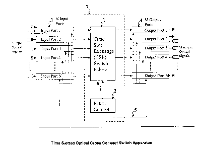
Figure 1 Time Slotted Optical Cross Connect Switch Apparatus
Figure 2 Operation of the Time Slotted Optical Cross Connect Switch Apparatus
Figure 3 Prior Art: Phase Lock Loop with Local Phase Detection
Figure 4 Remote Phase Detection Phase Lock Loop (RPD-PLL).
Figure 5 Support of wave division multiplexing by the time slotted optical
cross connect
switch .apparatus
Detailed Description of the Preferred Embodiments
In the preferred embodiment of the invention, which is shown in Figure 1, a
plurality of
input optical signals (N) are received by the apparatus at a plurality of
input ports 3. Each
input port 3 may receive a plurality of input optical signals. The optical
signals are, by
virtue o~f the function of input ports 3, packaged into a format that is
compatible with the
Time Slot Exchange Switch Fabric 1 (as will be described below) and
transmitted using
the Tune Slot Exchange Switch Fabric 1 to a plurality of output ports 4. At
the output
ports 4 the data that is received from the Time Slot Exchange Switch Fabric 1
is
converted back, by virtue of the function of output ports 4, to an outgoing
optical signal
as will be discussed below. Each output port 4 may emit a plurality of output
optical
signals. The number of outgoing optical signals M may be less than, bigger
than or equal
to the number of incoming optical signals, N. The connectivity map that
governs the
connectivity between input ports 3 and output ports 4, through the Time Slot
Exchange
Switch Fabric 1, is generated by the Fabric Control unit 2 and is conveyed to
the Time
Slot Exchange Switch Fabric 1 by the Configuration Signals 6. The connectivity
map
may be changed every time slot in order to allow each of the input ports 3 a
chance to
transmit data to different output ports 4. The Fabric Control unit 2 issues a
synchronization signal 5 that is conveyed simultaneously to all input ports 3
and output
ports 4. The synchronization signal 5 arrives at all input and output ports at
exactly the
CA 02339463 2001-03-06
same tame and is used to inform the ports of the start of each time slot. The
ports use this
synchronization signal 5 to commence the transmission and receipt of the data
through
the Tirne Slot Exchange Switch Fabric 1.
In Figure 1 the Time Slot Exchange Switch Fabric 1, the Fabric control unit 2
and the
Configuration Signals 6 form a Time Slot Exchange Switch 7. A preferred
embodiment
of this Time Slot Exchange Switch 7 are switches that are based on
"electrooptic wafer
beam dleflectors" which are disclosed in Patent Applictions "A Modular,
Expandable, and
Reconiigurable Optical Switch" by Leon-Garcia et al. [ALG-1], "A Time-Slotted
Optical
Space Switch" by Leon-Garcia et al. [ALG-2] and "Multiservice Optical Switch"
by
Leon-Garcia et al. (ALG-3]. Another preferred embodiment of the Time Slot
Exchange
Switch 7, are silicon-based electronic time slot exchange switches that are
constructed
using electronic systems that transmit data from input to output ports on a
time slot basis
similar to those described by [McKeown]. However, the operation of the current
apparatus is insensitive to the method by which the Time Slot Exchange Switch
is
implerr~ented. Any other methods of implementing time slot exchange switches
would
also be an embodiment of the Time Slot Exchange Switch Fabric 7.
Figure 2, which represents an embodiment of the present invention, depicts the
path of
one of the N incoming optical signals through the apparatus. Each input port 3
can
support: a plurality of Input Optical Signals 23. For the sake of clarity,
Figure 2 depicts
only one of the multiple Input Optical Signals that can be received at an
input port 3.
Upon the arrival of each Received Optical Signal 23 at an input port of the
apparatus, the
said Received Optical Signal 23 is converted, by the Optical Receiver Unit 10,
into two
signals of the electronic type: a Received Clock signal 12 and a Received Data
signal 11.
The Received Clock signal 12 contains the timing characteristics of the
incoming optical
signal, and the Received Data signal 11 contains the data that is carried
within the
incoming optical signal 23. The Received Data and the Received Clock signals
(11 and
12, respectively) take two different paths from the point of their creation to
the point
where they are finally merged into outgoing Transmit Optical signals) 22 at
the output
ports) 4. These two paths are described below.
Data Switching Path
The Received Data signal 11 of each Received Optical Signal 23 is queued into
one, or
several, Received Data First In First Out (RXD-FIFO) structures) 14. Each RXD-
FIFO
structure 14 represents a stream of data that will be eventually transmitted
out of the
apparatus as a Transmit Optical Signal 22 from an output port 4. If the
Received Data 11
is to exia the apparatus on a single Transmit Optical Signal 22, then the
Received Data 11
is writtc,n into the RXD-FIFO 14 that represents this single Transmit Optical
Signal 22.
If the Received Data 11 is to be transmitted out on several Transmit Optical
Signals 22,
from one or more Output Ports) 4, then identical copies of the Received Data
11 are
written into each of the RXD-FIFO(s) 14 that represent each of the outgoing
Transmit
Optical Signals 22.
7
CA 02339463 2001-03-06
Each input port 3 contains a Data Encapsulation Unit 15. The Data
Encapsulation Unit
15, shown in Figure 2, is an interface module that allows the input ports 3 to
communicate with, and to transmit data through, the Time Slot Exchange Switch
7. As
such, a description of the functions that are performed by the Data
Encapsulation Unit 15
follows. The first function of the Data Encapsulation Unit 15 is to monitor
the fill level of
the RX:D-FIFOs 14. Once the amount of data that is present in any given RXD-
FIFO 14
equals to or exceeds a threshold value that is related to the amount of data
that can be
transmitted through the Time Slat Exchange Switch 7 within the duration of one
time
slot, then the Data Encapsulation Unit 15 requests a Time Slot from the Fabric
Control
Unit 2 of the Time Slot Exchange Switch 7 through Request-Grant (RG) Signal
17. The
Fabric Control Unit 2 of the Time Slot Exchange Switch 7 arbitrates all the
requests for
time slats from all the RXD-FIFOs 14 an all input ports 3. Once the Fabric
Control Unit
2 decif.es to grant a Time Slot to a given RXD-FIFO 14 for transmitting the
data that is
contained in this RXD-FIFO 14, the Fabric Control Unit 2 transmits a Grant
Signal to the
said R~~D-FIFO 14, through the Request-Grant signal 17. The Fabric Control
Unit 2 then
config~:nes the Time Slot Exchange Switch Fabric 1 such that a path exists
from the input
port 3 .of the requesting RXD-FIFO 14 to the destination output port 4 from
which the
transmit optical signal 22 is to be transmitted from the apparatus. This
configuration of
the Tune Slot Exchange Switch Fabric 1 occurs through the Configuration
Signals 6.
The an-ival of the Grant Signal 17 from the Fabric Control Unit 2 informs the
Data
Encapsulation Unit 15 of the exact time slot at which it is allowed to
transmit data from a
specific; RXD-FIFO 14. Upon the receipt of this Grant Signal 17, the Data
Encapsulation
Unit 15~ waits until it receives the Synchronization Signal 5 from the Fabric
Control Unit
2. The arnval of the Synchronization Signal 5 indicates to all input ports 3
the start of a
Time Slot. Once a Synchronization Signal 5 is received, the Encapsulation Unit
15 reads
the data from the RXD-FIFO 14 whose request was granted by the Fabric Control
Unit 2.
The data which is read from the RXD-FIFO 14, using the data signal 38, is then
packagc;d, by the Data Encapsulation Unit 15, inta the time slot format of the
Time Slot
Exchange Switch 7. The value of the Received Clock Pulse Count Latch 28, which
represents the timing information of the incoming optical signal as will be
described
below, is also conveyed to the data encapsulation unit 15 via the timing
signal 37 and is
also packaged within the said time slot format of the Time Slot Exchange
Switch 7. One
notes that the data from the RXD-FIFO 14, and its corresponding timing
information, as
represented by the value of the Received Clock Pulse Count Latch 28 can be
transmitted
from the input port 3 to the corresponding output port 4 simultaneously within
the same
time slot or separately using two different time slats. The operation of the
apparatus is
insensitive to whether the RXD-FIFO 14 data and the value of the Received
Clock Pulse
Count batch 28, are conveyed to the output port 4 simultaneously or at
different points of
time. The formatted time slot information is then transferred from the Data
Encapsulation
Unit 15, to the Fabric Transmitter Unit 16 where the time slot information is
converted
into a signal type that is compatible with the type of signal that the TSE
Switch Fabric 1
uses. For example, if an "electrooptic wafer beam deflectors" based TSE Switch
Fabric is
used, the Fabric Transmitter Unit 16 would convert the time slot information
into an
optical signal. Alternatively, if an electronic-based TSE switch Fabric is
used, then the
8
CA 02339463 2001-03-06
Fabric Transmitter Unit 16 would convert the time slot information into an
electronic
format that is compatible with the input-output standard of the TSE switch
Fabric.
The information that is contained in the time slot, which is emitted by the
Fabric
Transmitter Unit 16, is switched by the action of the TSE switch fabric and
arrives at the
destination Output port 4 where it is received at the Fabric Receiver Unit 18.
The said
Fabric Receiver Unit 18 converts the incoming signal into an electronic format
that is
undersl;ood by the Data Extraction Unit 19 and forwards the time slot
information to the
said the Data Extraction Unit 19. The task of the Data Extraction Unit 19 is
to extract the
data anal the value of the Receive Clock Pulse Count Latch 28 that are
embedded in the
time slot format. As will be described below, the value of the Received Clock
Pulse
Count Latch 28 is conveyed to the Copy of Received Clock Pulse Count latch 30
in the
output port 4 via the signal 39. The data that is contained in the time slot
is conveyed to a
transmia data FIFO (TXD-FIFO) 20, via a connecting signal 41, where it is
stored. Each
output port 4 may contain several TXD-FIFOs 20. Each of these FIFOs represents
a
different outgoing optical Signal 22. For the sake of clarity, in Figure 2 we
show only one
of the multiple possible Transmit Optical Signals 22 that may be emitted by an
output
port 4.
For each Transmit Optical Signal 22 that is emitted by the output port 4, a
unique
Transmit Clock 25, which is constructed especially for the specific Transmit
Optical
signal, is then used to read the data from the TXD-FIFO 20. As will be
described below,
each unique Transmit Clock 25 is an equivalent copy of the Received Clock 12
of the
Receivc;d Optical Signal 23 that corresponds to the Transmit Optical Signal 22
that is
being l;enerated using this said unique Transmit Clock 25. The data that is to
be
transmitted is read, via Transmit Data sigmal 40, from the TXD-FIFO and is
then
combined with the Transmit Clock 25 by the Optical Transmitter Unit 21 to
generate the
Transmit Optical Signal 22, which now contains the same data that was received
in the
Received Optical Signal 23, and also has the same timing properties as the
Received
Optical Signal 23 since it is transmitted using the Transmit Clock 25 that is,
in turn, a
replicated version of the Received Clock 12. The sequence of the transmit
optical signal
22 is al~.so equivalent to that of the received optical signal 23 since data
is transmitted
from a given RXD-FIFO 14 on a given input port 3 to a corresponding TXD-
FIFO(s) 20
on corresponding output ports) 4 in order of arrival into the input port 3.
This order
guarantees that no out of sequence transmissions occur between the input ports
3 and the
output ports 4.
Clock Switching Path
As described above, each given Transmit Optical Signal 22 will correspond to a
unique
Receivc;d Optical Signal 23 when the content and timing of the said Transmit
Optical
Signal 22 are identical to those of the said Received Optical Signal 23. The
method by
which the content of the said Received Optical Signal 23 is conveyed into the
corresponding Transmit Optical Signal 22 has been disclosed above. The
following text
discloses a method by which the Transmit Clock signal 25 is created such that
it is a
replica of a specific Receive Clock signal 12. By achieving this, we are able
to ensure
9
CA 02339463 2001-03-06
that a given Transmit Optical Signal 22 will correspond to a unique Received
Optical
Signal 23 in terms of content, timing and sequence.
The method by which the Receive Clock signal 12 is replicated, in one or more
output
ports 4~, to produce one or more Transmit Clock signals 25 is based on the
well-known
discipline of Digital Phase Locked Loops (see [BEST] and [GARDNER]). The basic
operation of a Phase Locked Loop (PLL), including Digital Phase Locked Loop,
is
illustrated using Figure 3. The operation of the PLL is based on comparing the
phase of
an incoming clock 60 to that of the local clock 66 using a Phase Detector
apparatus 61.
The difference between the phases of the two clocks is conveyed to Loop Filter
apparatus
63 using the phase difference signal 62. T'he phase difference signal 62 may
be in an
analog or digital form (see [G.ARDNER] and [BEST]). Similarly, the Loop Filter
apparatus 63 may be an analog electronic circuit, a digital electronic circuit
or a software
program that runs on a hardware platform. 'The Loop Filter 63 maintains a
history of the
values of the phase difference signal 62 over a period of time and adjusts the
value of a
control signal 64 to minimize the phase difference between the incoming clock
60 and the
local clock 66. The control signal 64, which may be an analog or a dilrital
signal, is then
used to adjust the frequency of a Voltage Controlled Oscillator 65 that
generates the local
clock Ei6. The function of the Loop Filter 63 is to control the output of the
Voltage
Controlled Oscillator 65, which is the local clock 66, such that the frequency
and phase
of the incoming clock 60 and local clock 66 are matched over long periods of
time.
Common forms of Digital Phase hocked Loop circuits that have been used in the
telecom
industr,~ are usually used to generate one or multiple local clocks that are
all replicas of a
single instance of a master clock that is provided to the apparatus from an
outside source
(see for example [MUNTER]). In such applications, the incoming clock 60 and
the local
clock 66 are physically co-located. As such, the process of detecting the
phase difference
between the two clocks is implemented by comparing the two co-located clocks
in a
direct manner as described in [GARDNER] and [MUNTER]. We refer to these types
of
PLLs here as "Local Phase Detection PLLs" (LPD-PLL).
However, in the invention disclosed herein, the incoming clock 60 (which is
represented
by the receive clock 12 in the apparatus disclosed herein) and the local clock
66 (which is
equivalent to the transmit clock 25 in the apparatus disclosed herein) are not
co-located
and, thus, a simple phase detection, similar to that described in [GARDNER],
is not
feasible. To ensure that a local clock can be phase locked to an incoming
clock when the
two clocks are not co-located, we now disclose a novel Digital Phase Locked
Loop
apparah~s that we will refer to as "Remote Phase Detection Phase Lock Loop"
(RPD-
PLL). 'The Remote Phase Detection PLL, that we disclose herein, allows us to
replicate
an incoming clock to generate one or more local clocks) without having to co-
locate the
two clocks so that a direct comparison of the phase difference between the
incoming and
local clocks) can be performed.
Figure ~4 depicts a preferred embodiment of the Remote Phase Detection Phase
Lock
Loop (R:PD-PLL) that is disclosed in this patent. Here, the Incoming Clock 70
is used to
increment a Received Clock Pulse Counter 71. The said Received Clock Pulse
Counter
CA 02339463 2001-03-06
71 may be incremented once every single or multiple clock cycles of the
Incoming Clock
70. The value of the Received Clock Pulse Counter 71 is latched into a
Received Clock
Pulse Count Latch 72 at regular or irregular instances of time that are
defined by the
arnval of a Latch Synchronization Signal 74. The said Latch Synchronization
Signal 74 is
generated from a stable Reference Oscillatar 73. The Received Clock Pulse
Count Latch
72 may latch in the count value of the Received Clock Pulse Counter 71 every
time a
single Latch Synchronization Signal 74 is detected or it may perform the
latching
periodically with a period that is defined as the time required to observe a
defined
number of occurrences of the Latch Synchronization Signal 74, including
periods of time
that are not integer increments of the occurrence period of the Latch
Synchronization
Signal 74. The time period between two consecutive latching events of the
Received
Clock :Pulse Count Latch 72 will be referred to herein as the "Received Clock
Latching
Period". The Received Clock Pulse Counter 71 may be reset to a pre-determined
value
upon the latching of its value into the Received Clock Pulse Count Latch 72,
or,
alternatively, it may be allowed to free-run and wrap-around whenever it
reaches its
maximum count. The apparatus disclosed herein is insensitive to either forms
of
operation of the Received Clock Pulse Counter 71. Here, we note that the
Received Clock
Pulse C',ounter 71 and the Received Clock Pulse Count Latch 72 are physically
co-located
in a location that we will refer to as "Location A".
The value that is latched within the Received Clock Pulse Count Latch 72 is
distributed,
on periodic or non-periodic basis, using a transport mechanism 82, to all
remote locations
where a copy of the Incoming Clock 70 is required. For the sake of simplicity,
we show
only on.e of such locations in Figure 4, Location B. However, this does not
preclude the
existence of, and the distribution of the value of the Received Clock Pulse
Count Latch
72 to, nnultiple other remote locations that require a local copy of the
incoming clack 70.
The transport mechanism 82, which is used for distributing the value of the
Received
Clock :Pulse Count Latch 72 may be one of a variety of methods such as
software
messaging or the operation of hardware switches similar to, but not limited
to, a Time
Slot Exchange Switch 7. Upon the arrival of the value of the Received Clock
Pulse Count
Latch T2 to Location B, this value is latched into the local copy of the
received clock
pulse count latch 75. The apparatus in Location B includes a Voltage
Controlled
Oscillator (VCO) 78 that generates the Local Clock 79 that is a replica of the
incoming
clock 7~0. The local clocle 79 is used to increment a Local Clock Pulse
Counter 80. The
said Local Clock Pulse Counter 80 may be incremented once every single or
multiple
clock cycles of the Local Clock 79. The value of the Local Clock Pulse Counter
80 is
latched into a Local Clock Pulse C:'ount Latch 81 at regular or irregular
instances of time
that are defined by the arrival of the Latch Synchronization Signal 74. The
said Latch
Synchronization Signal 74 is generated from the stable Reference Oscillator 73
and is
distributed to all locations of the RPD-PLL. The Local Clock Pulse Count Latch
81 may
latch in the count value of the Local Clock Pulse Counter 80 every time a
single Latch
Synchronization Signal 74 is detected or it may perform the latching
periodically with a
period that is defined as the time required to observe a defined number of
occurrences of
the Latch Synchronization Signal 74, including periods of time that are not
integer
increments of the occurrence period of the Latch Synchronization Signal 74.
The time
period between t vo consecutive latching events of the Local Clock Pulse Count
Latch 81
11
CA 02339463 2001-03-06
will be referred to herein as the "Local Latching Period" and is a function of
the
"Received Clock Latching Period". The Local Clock Pulse Counter 80 may be
reset to a
pre-determined value upon the latching of its value into the Local Clock Pulse
Count
Latch 81, or, alternatively, it may be allowed to free-run and wrap-around
whenever it
reache s its maximum count. The apparatus disclosed herein is insensitive to
either form
of operation of the Local Clock Pulse Counter 80. Here we note that the Local
Clock
Pulse (:ounter 80 and the Local Clock Pulse Count Latch 81 are physically co-
located at
the location where the desired Local clock 79 is to be generated in a location
that we have
referred to as Location B. The value of the Local Clock Pulse Count Latch 81
and the
local copy of the received clock pulse count latch 75 are presented to the
Control Voltage
Generator 76 module which stores their respective values and uses the
historical
variations in these values to generate a digital voltage control signal 83.
The said digital
voltage: control signal 83 is converted into an analog voltage by an optional
Digital-to-
Analog; converter 77 that converts it into an analog voltage control signal
84. The said
analog voltage control signal 84 is then used to control the frequency output
signal 79 of
the VCO 78, that is, the local clock 79, if the VCO 78 is an analog component.
If the
VCO T8 is a digital component then the digital voltage control signal 83 is
connected
directly to the said digital VCO 78 and the need for an intermediate Digital-
to-Analog
converter 77 between 76 and 78 is eliminated. As such, the Control Voltage
Generator
76 module performs the function of a Loop Filter 63 in that it is used to
adjust the value
of a digital voltage control signal 83 to minimize the phase difference
between the
incoming clock 70 and the local clock 79. This phase difference is minimized
when
values of the Local Clock Pulse Count batch 81 and the local copy of the
received clock
pulse count latch 75, normalized to the values of the local latching period
and the
received clock latching period, respectively, are equivalent for long periods
of time. A
variety of algorithms exist for implementing the loop filter function that is
performed by
the Control Voltage Generator 76 (for example see [BEST] and [MUNTER]). The
Control Voltage Generator may be implemented directly in electronic hardware
or may
be a soi'tware entity that is executed on a hardware platform.
The essence of the RPD-PLL apparatus that is disclosed herein is that instead
of
perforrr~ing a phase detection of two co-located incoming and local clocks, we
perform
the phase operation detection remotely, at the location of the local clock 79,
using an
intermediate clock that is observable to both the incoming and local clocks.
In the current
invention, this intermediate signal is the Latch Synchronization Signal 74. We
note that
the Reference Oscillator 73, which generates the Latch Synchronization Signal
74, may
or may not be co-located in Location A, B or any other location where a copy
of the
incoming clock 70 is generated. For the purpose of simplifying the
illustration, we have
chosen to depict the Reference Oscillator 73 that is not co-located with 71
and 72.
However, this does not preclude the co-location of the Reference Oscillator 73
in location
A, B or any other location where a copy of the incoming clock 70 is generated
locally.
Moreover, we note that the even though, for the sake of ease of illustration,
the function
of the (:ontrol Voltage Generator 76 is shown to exist in Location B in Figure
4, this
depiction does not preclude any embodiment of the RPD-PLL wherein the function
of the
said Control Voltage Generator 76 is located in any location other than the
location where
12
CA 02339463 2001-03-06
the Local Clock 79 is generated. In such embodiments of the RPD-PLL where the
Control Voltage Generator 76 is not co-located with the Local Clock 79, a
transport
mechmism is implemented to transport the values of the Local Clock Pulse Count
Latch
81 ands the Received Clock Pulse Count Latch 72 to the location where the
Control
Voltage Generator 76 exists and to transport the value of the digital voltage
control signal
83 to the specific locations) where the Local Clock 79 is generated.
Having; disclosed the operation of the RPD-PLL we now disclose the method by
which
RPD-PLLs are used, in the Time Slotted Optical Cross Connect Switching
Apparatus, to
create 'transmit Clock signals 25 that are replicas of specific Receive Clock
signals 12 to
ensure that a given Transmit Optical Signal 22 will correspond to a unique
Received
Optical Signal 23. Returning to Figure 2, we observe that once the Received
Clock Signal
12 is extracted from the Received Optical Signal 23, by the Optical Receiver
10, it may
then be passed through an optional local Phase Lock Loop 26 to de-fitter the
clock and to
increase/decrease the frequency of the Received Clock. Once this function has
been
perfornied, the Receive Clock signal 12, or the modified Receive Clock signal
42 in the
case wlhere there is an optional PLL 26, is replicated at one or more output
ports 4 by
means of an RPD-PLL. Referring to Figure 2, the components of the RPD-PLL are
distributed among the input port 3, the output port 4 and the Time Slot
Exchange Switch
7. In Figure 2, for the sake of clarity we show only one output port out of
the many
output ports that may require a copy of the Receive Clock signal 12. The
following is a
list of t:he components that make up the RPD-PLL within the preferred
embodiment of
the Tirr~e Slotted Optical Cross Connect Switch Apparatus depicted in Figure
2, and their
corresponding component in the RPD-PI~L depicted in Figure 4:
1. The: Received clock signal 12 (or 42 for the case where the PLL 26 exists)
cowesponds to 70.
2. The Receive Clock Pulse Counter 27 corresponds to and performs the function
of 71.
3. The Receive Clock Pulse Count Latch 28 corresponds to and performs the
function of
72.
4. The Synchronization Signal 5 corresponds to and performs the function of
Latch
Synchronization signal 74.
5. The Fabric Control Unit 2, in that it is responsible for generating the
Synchronization
Signal 5, corresponds to and performs the function of the Reference Oscillator
73.
6. The Time Slot Exchange switch 7, the Data encapsulation Unit 15, the Fabric
Transmitter unit 16, the Fabric Receiver unit 18 and the Data Extraction unit
19, in
their function of transfernng the value of 28 from the input port 3 to one or
more
output ports 4, corresponds to and performs the function of the transport
mechanism
82.
7. The Copy of the Receive Clock Pulse Count Latch 30 corresponds to and
performs
the vfunction of 75.
8. The Voltage Controlled Oscillator 35 corresponds to and performs the
function of 78.
9. The Digital-to-Analog Converter 34 corresponds to and performs the function
of 77.
10. The Transmit Clock Pulse Counter 33 corresponds to and performs the
function of 80.
11. The Transmit Clock Pulse Count Latch 32 corresponds to and performs the
function
of 81.
13
CA 02339463 2001-03-06
12. The Control Voltage Generator module 31 corresponds to and performs the
function
of 76.
13. The Transmit Clock 25 corresponds to and performs the function of 79.
It is important to note that in any given output port 4, a dedicated set of
the units 30, 34,
35, 33 and 32 are required to generate each unique Transmit Clock 25. Unit 31
may be
shared among the multiple Transmit Clocks 25 that are generated at this output
port 4, or
alternatively, it may be a dedicated resource that needs to be replicated for
each of the of
the Transmit Clocks 25 that are generated within the said output port 4.
As described above, in the process of implementing the RPD-PLL within the Time
Slotted Optical Cross Connect Switch Apparatus, we utilized the
Synchronization Signal
to perform the function of the Latch Synchronization signal 74 and the Fabric
Control
Unit 2, to perform the function of the Reference Oscillator 73, in addition to
their primary
function that is associated with the transfer of data through the Time Slot
Exchange
Switch 7, to minimize the complexity of the system through re-use of
components to
perform several unrelated tasks. However, this optimization step does not
preclude the
use of an additional dedicated Reference Oscillator instead of using the
Fabric Control
Unit 2 and additional dedicated signals for conveying the Latch
Synchronization Signal
to all input ports 3 and all output ports 4. These two dedicated resources,
when
implemented in addition to the Synchronization Signal 5 and the Fabric Control
unit 2, in
Figure 2 would create another preferred embodiment of the RPD-PLL within the
Time
Slotted Optical Cross Connect Switch Apparatus. Moreover, the Latch
Synchronization
Signal may be implemented by any signal or event that can cause the latching
of the
counts into the Receive Clock Pulse Count Latch 28 and the Transmit Clock
Pulse Count
Latch(s) 32 with a controlled time relationship between the latching of the
count into the
Receive Clock Pulse Count Latch 28 on the input port 3 and the latching of the
counts
into the; Transmit Clock Pulse Count Latch 32 on the corresponding output
ports 4.
Furthermore, another embodiment of the RPD-PLL(s) within the Time Slotted
Optical
Cross Connect Switch Apparatus disclosed herein exists where the individual
Control
Voltage Generators 31 are located in any locations) other than the output
ports) 4 where
the Transmit Clocks) 25 are generated. In such embodiments of the RPD-PLL
where the
Control Voltage Generator 31 is not co-located with the Transmit Clock 25, a
transport
mechanism, similar to but not limited to the Time Slot Exchange Switch, is
used to
transport the values of the Transmit Clock Pulse C'.ount Latch 32 and the
Received Clock
Pulse Count Latch 28 to the location where the Control Voltage Generator 31
exists and
to tran port the value of the digital voltage control signal, which is
produced by the
Control Voltage Generator 31, to the specific output ports) where the
Transport Clock 25
is generated.
A series of additional features are also supported by the Time Slotted Optical
Cross
Connect Apparatus disclosed herein:
1. In Figure 2, the Monitor unit 13 may examine the Receive Data signal 11 and
Receive
Clock signal 12. The Monitor unit 13 monitors the quality of the incoming
signal to
detect any failures of, or degradation in the quality of, the Received Optical
Signal
14
CA 02339463 2001-03-06
23. 'The Monitor unit 13 can also monitor the performance of specific
transmission
protocols such as, but not limited to, SONET, Ethernet, Packet over SONET
(POS),
Resilient Packet Ring or Digital Wrapper.
2. The Request component of the Request-Grant signal 17 may be removed from
the
design if the Fabric Controller 2 is configured to automatically issue the
Grant
component of the Request-Grant signal 17 to the Input Ports 3 at a rate that
is
engineered such that none of the RXD-FIFOs 14 are allowed to overflow nor are
any
of the TXD-FIFOs 20 allowed to underflow.
3. The use of the some input and output ports of the Time Slot Exchange Switch
7 for
the purpose of implementing the Time Slotted Optical Cross Connect Switch
Apparatus does not preclude the simultaneous use of other ports of the Time
Slot
Exchange Switch 7 for the purpose of supporting other switching functions such
as,
but not limited to, packet switching, cell switching and circuit switching.
4. The use of some of the RXD-FIFOs 14 and TXD-FIFOs 20 in input ports 3 and
ouput ports 4 ports, respectively, of the Time Slotted Optical Cross Connect
Switch
ApI>aratus for the function of implementing an optical cross connect switch
does not
preclude the simultaneous use of other RXD-FIFOs 14 and other TXD-FIFOs 20 on
the same input ports 3 and output ports 4 ports of the apparatus for the
purpose of
supporting other switching functions such as, but not limited to, packet
switching, cell
switching and circuit switching.
In the apparatus described herein, each input port 3 (or each output port 4)
can support a
number of Received Optical Signals 23 (or Transmit Optical Signals 22) such
that the
aggregate rate of incoming information to the input port 3 (or outgoing
information from
output port 4) is equal to or less than the aggregate rate of all the input
ports (or output
ports) of the Time Slot Exchange Switch 7 that are connected to the said input
port 3 or
output port 4 of the Time Slotted Optical Cross Connect Switch Apparatus. The
relationship between the number of Received Optical Signals 23 (or Transmit
Optical
Signal, 22) and the number of ports in the Time Slot Exchange Switch 7, is a
function of
the maximum aggregate rate of the incoming Received Optical Signals 23 into
one input
Port 3 (or the maximum aggregate rate of the outgoing Transmit Optical Signals
22 from
one output Port 4) and the transmission rate of each input/output port of Time
Slot
Exchange Switch 7. For example, if for one input port 3 the rate of each
Received
Optical Signals is one fourth that of the rate of the input/output port of the
Time Slot
Exchange Switch 7, then the input port 3 can support a maximum of 4 incoming
Received Optical Signals and transfer them all to various output ports using
only one
input port of the Time Slot Exchange Switch 7. In this case, the data from the
4 incoming
Received Optical Signals 23 are buffered in the RXD-FIFOs 14 and are then
transmitted
in a time-division multiplexed manner, which may or may not be in a periodic
or
repetitive manner, during 4 different time slots to their respective output
ports 4. In this
example, whenever data is transmitted through the fabric, it travels at 4
times the rate of
the incoming Receive Optical Signal 23 and therefore the overall rate of data
transfer
from tine RXD-FIFO through the Time Slot Exchange Switch 7 is equal to the
rate of the
Received Optical Signal. Therefore the RXD-FIFO would never overflow. In the
current
invention, we allow the input and output rates of the ports of the Time Slot
Exchange
Switch 7 to be higher than the minimum required rate, which is equal to the
aggregate
CA 02339463 2001-03-06
rate of the incoming Received Optical Signals 23 to an input port 3 that will
be
transmitted to output ports 4 on a single port of the Time Slot Exchange
Switch 7, or the
aggregate rates of the outgoing Transmit Optical Signals 22 from an output
port 4 whose
data will be received by 4 through a single port of the Time Slot Exchange
Switch 7, in
order to compensate for the overhead information that will be carried in the
time slot
(such as the value of the Received Clock Pulse Latch Counter 28 of the
Received Optical
signals :L3) and any switch reconfiguration period, when no valid data is
allowed to pass
between the input and output ports of the time slot exchange switch fabric.
Furthermore, the Time Slotted Optical Cross Connect Switch Apparatus that is
disclosed
herein is capable of switching optical signals that have been concentrated by
means of a
wave division multiplexes. As shown in Figure 5, when a wave division
multiplexes 8,
which is external to Time Slotted Optical Cross Connect Switch Apparatus, is
added prior
to the apparatus in order to concentrate multiple optical signals into a
single optical
signal, then at each of the input ports 3 of the Time Slotted Optical Cross
Connect Switch
Apparatus, the constituent optical signals that make up the said incoming wave
division
multiplexed optical signals are wave division de-multiplexed and each of the
said de-
multiplexed constituent optical signals are converted into a Receive Clock
signal 12 and a
Receive; Data signal 11 within each of the input ports 3, by the operation of
the Optical
Receivc;r Unit 10. As such, in this embodiment of the invention, there exists
a wave
division de-multiplexes within the Optical Receiver Unit 10. The Receive Clock
signal 12
and the Receive Data signal 11 of each of the received optical signals are
then switched
to their respective output ports 4, as described above using dedicated RXD-
FIFOs 14,
TXD-FIFOs 20 and RPD-PLLs for each signal. At output ports) 4 the constituent
clock
and data signals of the individual optical signals, 25 and 40, are recombined
into the said
optical signals, by the action of the Optical Transmitter 21, and a plurality
of these
generated optical signals are then wave division multiplexed into an outgoing
Transmit
Optical Signal 22, also by the action of the Optical Transmitter 21, and
emitted from the
output port 4. The constituent components of this outgoing wave division
multiplexed
signal may be recovered by passing the signal through a wave division de-
multiplexes 9
that is external to the Time Slotted Optical Cross Connect Switch Apparatus.
Alternatively, a wave division multiplexed incoming optical signal 100 that is
received
by the 'Time Slotted Optical Cross Connect Switch Apparatus, may be first
passed though
a wavf; division de-multiplexes unit 101, which is a part of the Time Slotted
Optical
Cross Connect Switch Apparatus and which may or may not be co-located with any
of
the input ports 3 (in Figure 5, we show the case where 101 is not co-located
with any of
the input ports 3 to simplify the figure). The said wave division de-
multiplexes unit 101
de-multiplexes the incoming wave division multiplexed incoming optical signal
100 into
its constituent optical signals 106 and transmits these incoming optical
signals into the
plurality of input ports 3. Through the aforementioned operation of the Time
Slotted
Optical Cross Connect Switch Apparatus, these optical signals 106 are switched
and
arrive at their corresponding output ports where they may be emitted as non-
wave
division multiplexed optical signals or as part of a wave division multiplexed
optical
signal. In a similar manner, a plurality of non-wave division multiplexed
optical signals
105 may be wave division multiplexed into a single outgoing waved division
multiplexed
16
CA 02339463 2001-03-06
optical signal 104 by the actions of a wave division multiplexer unit 103
which is part of
the Time Slotted Optical Cross Connect Switch Apparatus and which may or may
not be
co-locat:ed with any of the output ports 4 (in Figure 5, we show the case
where 103 is not
co-locat:ed with any of the output ports 4 in order to simplify the figure).
17