Note: Descriptions are shown in the official language in which they were submitted.
CA 02339653 2001-02-05
WO 00/17805 PCT/EP99/06887
ELECTRICAL CONNECTOR FOR AN ELECTRONIC-MEMORY CARD OR SMART CARD
The present invention relates to an electrical connector for
a contact-type smart card of rectangular general shape.
s The invention relates more particularly to a connector of
the typevcomprising a support made of insulating material which
defines a housing open in its upper face, this housing being
bounded laterally by two parallel longitudinal edges and
transversely by at least one front bottom edge and
to accommodating a front portion of a card which is inserted into
the housing in a longitudinal direction parallel to its plane and
which, on its lower main face, includes conducting contact pads
which are arranged near the front transverse edge of the card
and which engage with the contact ends of electrical-contact
is elements arranged in the bottom of the housing of the support
when the card is in its contact position in which its front
transverse edge butts against the front transverse bottom edge
of the housing, and of the type in which the electrical-contact
elements are carried by the support.
2o Such an example of an electrical connector, sold by the
company ITT, is described and illustrated in the French Patent
Application FR-A-2,742,5fi1.
That document provides a connector for connecting a
standardized card of the MICROSIM type which is a small card.
2s Thus, the greater longitudinal part forming the front portion of the
card is accommodated in the housing of the connector support,
that is to say the lower face of the card extends virtually over the
entire area opposite the bottom of the housing formed in the
insulating support, only a small rear longitudinal portion of the
3o card projecting out of the housing, especially in order to be able
to make it easier to grip it.
CA 02339653 2001-02-05
WO 00/17805 PCT/EP99/06887
2
Moreover, the connection ends of the contact elements
extend in groups longitudinally to the front and respectively to
the rear of the insulating support, and beyond the front and rear
transverse faces of the latter, in order to engage with conducting
s tracks of a printed-circuit board which accommodates the
connector.
Finally, that document also proposes the arrangement of a
metal cover which is mounted so as to slide on the support and
which holds the card in the housing of the insulating support by
~o virtue of its main upper plate-shaped part which extends above
the upper face of the card when the latter is in place in the
housing.
The invention aims more particularly to provide a
connector suitable for connecting another type of card, also
is standardized, which especially makes it possible to store a large
amount of data in order thus to constitute a removable data
medium which is generally of small size but of high storage
capacity. Several embodiments of such a type of memory card,
also called a "flash" card, the dimensions of which are becoming
2o smaller and the storage capacity of which is becoming greater,
are known.
This is especially the case with the so-called " MMC"
(MuItiMediaCard) card sold by the company SANDISK, the
dimensions of whose body containing the integrated circuits and
2s the positioning of its conducting contact pads are specifically
defined by its manufacturer and by an association of users so as
to have a standardized-type definition of such a card. This
definition forms the subject, for example, of the publication
MuItiMediaCard System Specification Version 1.4 Official
~o Release @ February 1998 MMCA.
This type of MMC card is generally similar in its shape and
in its proportions to a MICROSIM card, especially in that it
CA 02339653 2001-02-05
WO 00/17805 PCT/EP99/06887
3
includes polarizing means for correctly and unambiguously
positioning it in a connector and/or in a read/write device, which
consist of a cut corner formed at one of the corners of the card,
which is generally rectangular in shape. .
On the other hand, the contact pads on the MMC card
consist'of a series of adjacent conducting pads which are aligned
transversely along the short front end transverse edge of the
MMC card in which the polarizing cut corner is also formed.
However, the overall dimensions of the MMC card, or of
io other cards of the same type, are larger than those of a
MICROS1M card and the design of a connector proposed in the
above-mentioned French Patent Application is not perfectly
suitable for this type of card insofar as it results in a very large
overall size of the connector, this being a significant drawback
is insofar as the surface area occupied by the insulating support of
the connector on the upper face of a printed-circuit board on
which it is mounted is large, this surface area then being, of
course, no longer available for mounting other electronic
components on the printed-circuit board.
2o The invention therefore aims to provide a novel design of
electrical connector of the above-mentioned type which is
suitable for connecting a smart card, especially a card of MMC
type, and which remedies the above-mentioned drawbacks,
especially those relating to the size of the connector.
2s To this end, the invention provides a connector
characterized in that the electrical-contact elements have free
connection ends which all extend longitudinally beyond a rear
transverse face of the insulating support, beyond which face the
main portion of the body of the card extends rearwards in a
~o cantilevered fashion.
Thus, the overall dimensions of the connector are reduced
and the surface area of the printed-circuit board which extends
CA 02339653 2001-02-05
WO 00/17805 PCT/EP99/06887
4
beneath the main portion of the body of the card arranged so as
to be cantilevered from the connector may carry other electronic
components.
According to other characteristics of the invention
s - the length of the front portion of the card accommodated
in the housing bounded longitudinally by the said front transverse
bottom edge and by the said rear transverse face of the support
is less than the transverse width of the card ;
- the length of the front portion of the card accommodated
io in the housing bounded longitudinally by the said front transverse
bottom edge and by the said rear transverse face of the support
is equal to approximately one third of the length of the card ;
- the insulating support is extended longitudinally
rearwards, beyond the said rear transverse face, by two opposed
is lateral extensions in which the rear parts of the parallel
longitudinal edges of the housing are formed for guiding the card
laterally ;
- all the conducting pads on the card are aligned
transversely, especially along the front end transverse edge of
2o the card and the contact ends are aligned transversely apart from
at least one of these ends which is offset longitudinally
rearwards so that, when the card is inserted longitudinally from
the rear to the front into its housing, the corresponding
conducting pad on the card comes into contact with this offset
2s contact end before the other conducting pads on the card each
come into contact with one of the transversely aligned contact
ends ;
- it includes a metal cover for holding the card in the
housing which extends above the upper face of the card and
~o which is bounded longitudinally by two transverse edges, namely
a front transverse edge and a rear transverse edge, located
longitudinally approximately in line with the said front transverse
CA 02339653 2001-02-05
WO 00/17805 PCT/EP99/06887
bottom edge of the housing and in line with the said rear .
transverse face of the insulating support, respectively, and the
cover has tabs for fixing it, by soldering, to the upper face of a
board which carries the connector, especially on conducting
tracks connected to the earth plane of a printed-circuit board ;
-~t~e cover is made in the form of an upper plate which
extends above the upper face of the card and the parallel lateral
edges of which are extended by two flanges bent over
downwards for mounting the cover on the insulating support ;
io - the two mounting flanges form slideways allowing the
cover to be mounted on the insulating support by sliding in the
longitudinal direction ;
- the metal cover includes integrally formed retractable
means for providing longitudinal retention of the card in its
is housing, against the elastic return force which is applied to it by
a spring for automatically ejecting the card, which means engage
with at least one portion of the rear transverse edge of the card ;
- one of the said lateral extensions extends approximately
the entire length of a first lateral edge of the card, the said
2o retention means engage with that part of the rear transverse
edge of the card which is adjacent to the said first lateral edge
and the ejection spring engages with a portion of the front
transverse edge of the card adjacent to the second lateral edge
of the card ;
2s - the automatic ejection spring is made in the form of a
metal blade produced integrally with the metal cover ;
- the front transverse edge of the card has a corner cut at
approximately 45° and intended to engage with a corresponding
surface inclined at 45° formed at one of the ends of the front
~o transverse bottom edge of the housing in order to form polarizing
means defining a correct position for the card in the housing of
the connector ;
CA 02339653 2001-02-05
WO 00/I7805 PCT/EP99/06887
6
- it includes a switch for detecting the presence of the
card in the contact position in the housing ;
- the switch is carried by the insulating support and
includes an actuator for tripping it, with which a portion of the
s front transverse edge of the card engages ;
~t;)1e actuator is placed close to the said inclined surface
and the said portion of the front transverse edge of the card
consists of the cut corner of the card ;
- the switch is of the type normally closed in the absence
to of a card and comprises an elastically deformable switch blade
which is integrally produced with the metal cover and which
extends vertically and longitudinally from the upper plate of the
latter into the housing with its free end which, in the absence of
a card, is in elastic bearing contact against a contact end of one
is of the contact elements of the connector in order to establish a
switching circuit between the free connection end of this contact
element and an electrical earth plane to which the metal cover is
connected ;
- a switch tab of the cover extends horizontally below the
20 lower face of the insulating support opposite the free contact end
part of a contact element which is extended vertically downwards
by a switch blade, especially in the form of a loop, in order to
form a normally-open switching circuit which is closed upon
insertion of the card which causes the contact end to bend
?s elastically downwards in order to bring the loop into contact with
a facing portion of the said switch tab of the cover ;
- the upper plate of the cover has as many test holes as
there are contact ends with offset test holes opposite the offset
ends.
~o The invention also provides a double connector for
connecting two similar smart cards arranged so as to be parallel,
one above the other, of the type comprising a lower connector,
CA 02339653 2001-02-05
WO 00/17805 PCT/EP99/06887
7
which is made according to any one of the preceding claims and
which accommodates a lower card, and an upper connector
which lies on top of the lower connector and accommodates the
upper card, the design of the upper connector being generally
s similar to that of the lower connector except for its contact
elemen~~ which extend, from the contact ends, longitudinally
forwards with their free connection ends which extend
longitudinally forwards beyond the front end transverse face of
the insulating support of the lower connector and then vertically
to downwards, at least as far as level with the lower face of the
insulating support of the lower connector.
According to other characteristics of the double
connector
- the two cards are aligned longitudinally when they each
is occupy their contact position ;
- it includes a single metal cover common to both
connectors in order to hold them in the superposed position and
for fixing the double connector by soldering ;
- the upper connector includes a switch of the normally
2o closed type and the lower connector includes a switch of the
normally-open type, the two switches having a common point
connected to an earth plane via the common cover.
Other characteristics and advantages of the invention will
appear upon reading the detailed description which follows, for
2s the comprehension of which reference will be made to the
appended drawings in which
- Figure 1 is a top and three-quarter rear perspective view
which illustrates a connector according to the invention, shown in
the position mounted on a printed-circuit board and in
~o association with an MMC-type card in the approach position for
the purpose of inserting it into the connector ;
CA 02339653 2001-02-05
WO 00/17805 PCT/EP99/06887
8
- Figure 2 is a top view of the connector in Figure 1, in
which the card is illustrated in the inserted connection position in
the connector ;
- Figure 3 is a top view similar to that in Figure 2, in which
s the connector is illustrated without a card ;
Figure 4 is a longitudinal sectional view on the line 4-4 in
Figure 3 ;
- Figure 5 is a side view in the direction of the arrow F5 in
Figure 3 ;
to - Figure 6 is a longitudinal end view in the direction of the
arrow F6 in Figure 3, with a detailed part illustrated in cross
section on the line 6-6 in Figure 4 ;
- Figure 7 is a perspective view on a larger scale of the
connector illustrated in Figure 1, including modifications making
is it easier to fit its metal cover ;
- Figure 8 is a top view which illustrates only the metal
cover of the connector ;
- Figure 9 is a bottom view of the cover of the connector ;
- Figure 10 is an end view in the direction of the arrow F10
2o in Figure 8 ;
- Figure 11 is a top and three-quarter rear perspective
view which illustrates a first variant of the connector according to
the invention, comprising retractable means for retaining the card
in the connection position in the connector opposing an ejection
2s force applied to the card by an ejection spring, the card being
shown in Figure 11 in this position in its housing in the connector
- Figure 12 is a view similar to that in Figure 11, in which
the card is illustrated in a position in which it is partially ejected
~o from the connector ;
- Figure 13 is a view similar to that in Figure 12, which
shows the connector without a card ;
CA 02339653 2001-02-05
WO 00/17805 PC'T/EP99/06887
9
- Figure 14 is a view similar to that in Figure 13, which
shows the connector without its metal cover ;
- Figure 15 is a top and three-quarter rear perspective
view which illustrates a variant of the connector illustrated in
s Figure 12 which differs from it due to the design of the spring for
automafi~~ally ejecting the card ;
- Figures 16 and 17 are views similar to those in Figures 3
and 6, which illustrate another variant of a connector according
to the invention with regard to a first embodiment of a switch for
to detecting the presence of a card in the contact position ;
- Figures 18 to 20 are views similar to those in Figures 3,
4 and 6, which illustrate another variant of a connector according
to the invention, comprising another embodiment of a switch for
detecting the presence of a card in the contact position ;
is - Figures 21 and 22 are views similar to those in Figures
18 and 20, which also illustrate another variant of a connector
according to the invention comprising another embodiment of a
switch for detecting the presence of a card in the contact position
20 - Figures 23A, 23B and 23C are three similar views, in
longitudinal section on the line 23-23 in Fiaure 21. which
illustrate three successive longitudinal insertion positions of the
card in its housing ;
- Figure 24 is a view on a larger scale of the detail D24 in
2s Figure 21, with partial cut-away of the corresponding portion of
the cover of the connector ;
- Figure 25 is a top and three-quarter front perspective
view which illustrates a double connector made according to the
teachings of the invention with its two cards, namely the lower
~o and upper cards, in the contact position, the connector being
shown mounted on the upper face of a printed-circuit board ;
CA 02339653 2001-02-05
WO 00/17805 PCT/EP99/06887
- Figure 26 is a view similar to that in Figure 25, in which
the connector is illustrated in its metal cover ;
- Figure 27 is a view similar to that in Figure 26, in which
the connector is illustrated without an upper card;
s - Figure 28 is a view similar to that in Figure 27, in which
the connector is illustrated without a lower card ;
- Figure 29 is a top and three-quarter front perspective
view of the connector shown in Figure 28 ;
- Figures 30 to 33 are views similar to those in Figures 3
Io to 6, which relate to the double connector illustrated in Figure 25
but shown without any card ;
- Figure 34 is a top and three-quarter rear perspective
view which shows the lower connector of the double connector in
Figure 25 ;
is - Figure 35 is a top and three-quarter rear perspective
view which shows the upper connector of the double connector in
Figure 25 ;
- Figure 36 is a three-quarter front perspective view of the
upper connector in Figure 35 ;
- Figure 37 is a bottom and three-quarter rear perspective
view of the upper connector in Figure 35 ;
- Figure 38 is a top and three-quarter rear perspective
view of the cover of the double connector in Figure 25 ;
- Figure 39 is a top and three-quarter rear perspective
2s view which illustrates a double connector according to the
invention of the type illustrated in Figure 25, but having a
modified cover incorporating a switch blade for detecting the
presence of the upper card ;
- Figure 40 is a bottom and three-quarter rear perspective
~o view illustrating the cover of the double connector illustrated in
Figure 25 and showing a modification of its lower part in order to
CA 02339653 2001-02-05
WO 00/17805 PCT/EP99/06887
11
form a switch for detecting the presence of the lower card in the
connector ; and
- Figure 41 is a diagrammatic representation of the lower
face of an MMC-type card.
s !n the description which follows, identical, similar or
analogo:u~s components will be denoted by the same reference
numbers.
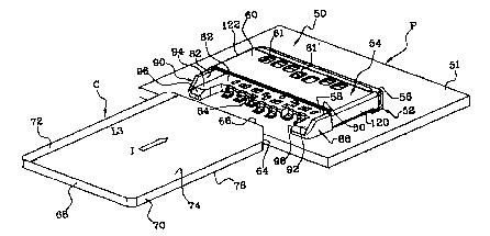
Figure 1 shows an electrical connector 50 made according
to the teachings of the invention, which connector is illustrated in
io the position mounted in and fixed to the upper face 52 of a board
P which carries the connector 50 and which is, for example, a
printed-circuit board whose upper face 52 has conducting tracks,
not shown in detail in the figures.
The connector 50 essentially consists of a generally plate
Is shaped insulating support 52 made of plastic and of a metal
cover or lid 54 which especially extends above the plane and
horizontal upper face 56 of the insulating support 52 in which is
formed a card housing 58 which is open vertically upwards
opposite the upper plate-shaped main part 60 of the cover 54.
2o The housing 58 is bounded vertically downwards by a
horizontal lower bottom wall 62 and it is open longitudinally
rearwards in order to present a slot for the longitudinal insertion
of the front portion of an electronic-memory card C which, for
example, is an MMC-type card.
2s The card C, of known design, has a rectangular general
shape bounded longitudinally by a front end transverse edge 66,
by a rear end transverse edge 68 and by two parallel and
opposed lateral edges 70 and 72.
The front corner corresponding to the intersection of the
~o edges 66 and 70 is a standardized 45° cut corner 64 for
polarizing the position and orientation of the card C.
CA 02339653 2001-02-05
WO 00/17805 PCT/EP99/06887
12
Moreover, the card C has a horizontal free upper face 74 .
and an opposed and parallel lower face 76 which is oriented
downwards in the direction of the printed-circuit board and which
has (see Figure 41 ), near its front end transverse edge 66, a
s series of seven conducting contact pads 77 and 77' which are all
alignedv.~~ransversely and which are adjacent to the front end
transverse edge 66. According to one aspect of the invention, the
contact pads 77 and 77' are oriented downwards in the direction
of the printed-circuit board P.
~o The card C is thus able to be inserted, in the direction I
indicated in Figure 1, from the rear to the front into the housing
58 until its front transverse edge 66 butts against a front
transverse bottom edge 78 by which the housing 58 is bounded
at the front.
is The opposed lateral edges 70 and 72 of the card C are
slidingly guided in the housing 58 by parallel and opposed
longitudinal edges 80 and 82 respectively (see Figure 14) by
which the housing 58 is bounded transversely.
As may be seen in the figures, the housing 58 proper, in
2o which the front portion of the card C is accommodated, is
bounded transversely at the front by the front transverse bottom
edge 78 and transversely at the rear by a rear end transverse
face 84 of the insulating support 52.
Moreover, the insulating support 52 is bounded
2s transversely at the front by a front transverse face 86.
In order to improve the lateral sliding guidance of the card
C as it is being inserted into or extracted from the housing 58,
the body of the insulating support 52 has two opposed
longitudinal extensions 88 and 90 which extend longitudinally
~o rearwards beyond the rear transverse face 84 in order to
increase the length of the longitudinal guiding edges 80 and 82.
CA 02339653 2001-02-05
WO 00/17805 PCT/EP99/06887
13
The extensions 88 and 90 also have horizontal parts 92 .
and 94 which extend the plane of the bottom 92 with an insertion
chamfer 96.
In order to fulfil the function of polarizing the position and
s orientation of the card C, the corner of the housing 58
corresp.o~nding to the intersection of the front transverse bottom
edge 78 with the longitudinal edge 80 has a vertical face 98
inclined at 45° which is complementary to the shape and to the
size of the cut corner 64 as may be seen in Figure 2, when the
to card C is inserted into the correct position.
According to a known technique in the field of connectors
for connecting printed-circuit boards, the insulating support 52
carries a series of electrical-contact elements 100 which are
made in the form of elastically deformable blades, a free contact
Is end 102 of which projects vertically above the plane of the
bottom 62 in order to engage with the conducting pads on the
lower face 76 of the card C.
In the example illustrated in the figures, there are seven
elastic contact blades 100, this being equal to the number of
2o contact blades 77 and 77', five of these blades 100 being aligned
transversely near the front transverse bottom edge 78 of the
housing 58 whereas the other two blades 100' are offset
longitudinally rearwards so that their two contact ends 102' are
offset longitudinally rearwards.
?s The purpose of this offset is to comply with a requirement
pertaining to the standardization of the method of connection to
the MMC card, which requires two special contact pads 77' to be
connected to a power supply before the other pads are
connected. For this purpose, the two contact ends 102' are offset
~o longitudinally rearwards with respect to the contact ends 102 of
the other five contact elements 100 and in the same way their
CA 02339653 2001-02-05
WO 00/17805 PC't/EP99/06887
14
associated connection ends 104' are offset longitudinally
rearwards with respect to the other five connection ends 104.
All the contact blades 100 and 100' are identical and each
has a rear free connection end 104, 104' which terminates
s approximately in line with the rear transverse face 84, each end
104, 104 being designed here in the form of a lead to be
soldered onto the surface of the upper face 51 of the printed-
circuit board P.
Because of the rearward longitudinal offset of two elastic
to blades 100', the insulating support has a corresponding
extension 106 which extends longitudinally rearwards slightly
beyond the vertical plane corresponding to the rear transverse
face 84.
The length of the aligned contact pads 77 and 77' is such
is that it makes it possible to obtain a reliable electrical connection
to all the pads when the card is in the butted contact position,
despite the slight offset of the ends 102'.
As may be seen especially with regard to Figures 3 and 4,
the total length L1 of the housing 58 which accommodates the
2o front portion of the card C is markedly less than the transverse
width L2 of the housing 58 which itself is approximately equal to
the transverse width of the card C.
Moreover, the transverse length L1 bounded by the front
transverse bottom edge 78 and the rear transverse face 84 here
2s is substantially equal to about 1/3 of the total length L3 of the
card C.
Thus, as may be seen more particularly in Figure 2, it is
the approximately two thirds of the card C which extend
longitudinally rearwards out of the housing 58 so as to be
~o cantilevered above the facing portion of the upper face 51 of the
board P.
CA 02339653 2001-02-05
WO 00/17805 PCT/EP99/06887
As may also be seen in Figures 3 and 4, the length of the .
upper plate 60 of the cover 54, bounded by its front transverse
edge 108 and its rear transverse edge 110, is also approximately
equal to the length L1 of the housing 58, that is to say its edges
s 108 and 110 extend approximately in line with the front
transve~r.~e bottom edge 78 and with the rear transverse face 84
of the insulting support 52.
By virtue of this dimensioning of the cover 54, the
connection ends 104 and 104' are completely clear (see Figure
io 2) and visible in order to facilitate the infrared soldering
operations and to allow a visual inspection of the soldered joints
as well as a possible subsequent repair, by manual intervention.
Moreover, the lateral extensions 88 and 90 protect all the output
leads 104 and 104' during manufacture and transportation of the
Is connectors.
As may be seen especially in Figure 4, the free connection
ends 104 and 104' lie substantially in the plane of the lower
plane face 57 of the insulating support 52.
According to a general design known, for example, from
2o the above-mentioned French patent application, the metal cover
54 has, in order to mount it on the insulating support 52, two
parallel and opposed lateral flanges 120 and 122 which extend
vertically downwards along corresponding portions 116 and 118
of the vertical external longitudinal faces of the insulating
zs support 52 {see Figure 14, for example).
The flanges 120 and 122 are shaped so as to form
slideways, that is to say they are extended horizontally beneath
the insulating support 52 by inwardly-bent horizontal branches
124 and 126 which are accommodated in corresponding housings
~o formed in the lower face 57 of the insulating support 52 so as not
to extend beyond the plane of this face.
CA 02339653 2001-02-05
WO 00/17805 PCT/EP99/06887
16
According to one characteristic of the invention, the cover
54 has, near its front transverse edge 108, two lower horizontal
tabs 132 and 134 which extend from the flanges 120 and 122 in
order to be accommodated in recesses 136 in the lower face 57
s so that the tabs 132, 134 can be soldered, for example by reflow
solderirl.g, to the corresponding conducting tracks on the printed
circuit board P (these not being shown) which are preferably
connected to the earth plane of the electrical circuit of the
printed-circuit board so as to electrically connect the metal cover
~0 54 to this earth plane.
Mechanically fastening, by soldering, the cover 54 by
means of its soldering tabs allows the connector 50 to be
mechanically held in place at its front part, without requiring the
use of any additional piece or component. In addition, this
~s fastening of the front part balances the fastening of the rear part,
provided by the soldering of the output leads 104, 104'. The gap
between the cover 54 and the insulating support 52 makes it
possible to achieve automatic centring positioning when the
connector is put into place in order to solder it with its front part
2o having the soldering tabs which always come into contact.
In addition, the cover 54 compensates for the forces
involved if a user attempts to lift the card C which then bears
against the plate of the cover 54 which is soldered to the board
P, no force being transferred to the support 52 or to the output
zs leads 104 and 104'.
In the variant illustrated in Figures 12 to 14, the connector
50 includes a first embodiment of means for automatically
ejecting the card C which has, according to a design known
especially from French Patent Application No. 98/06852, to the
~o content of which reference may be made in order to understand
the embodiment details thereof, an ejection spring 140 which
here is a helical compression spring mounted in a semi-
CA 02339653 2001-02-05
WO 00/17805 PCT/EP99/06887
17
cylindrical housing 142 open to the top and formed in the bottom .
62 of the housing 58 and partly in a rear longitudinal extension
144 of the insulating support which is arranged laterally in the
extension of the rear longitudinal extension 90 in line with the
s lateral side 72 of the card C.
T~~,e automatic ejection means also include a retractable
retention lip or tab 146 which, in the inserted position of the card
illustrated in Figure 11 and against the force which is applied by
the spring 140 to the front transverse edge 66 of the card C,
~o provides longitudinal retention of the latter inside the housing 58.
If the retention tab 146 is retracted, as illustrated in
Figure 12, the compressed spring 140 relaxes and causes total
or partial ejection of the card C out of the housing 58.
In order to allow the arrangement of the retention tab 146,
is the rearward longitudinal extension 88 of the insulating support
52, which lies on the opposite side to the extensions 90 and 144
that are adjacent to the point of action of the spring 140 on the
front transverse edge 66 of the card C, extends substantially
over the entire length of the lateral edge 70 of the card C, as
2o may be seen in Figure 11.
Thus, the action of the spring 140, which tends to make
the card C pivot in a swinging motion in its plane about a vertical
axis, is counteracted by the very long internal longitudinal
guiding edge 80 which extends over the entire length of the
2s rearwardly elongate longitudinal extension 88.
The variant illustrated in Figure 15 differs from the
previous one only by the design of the ejection spring 140, which
here is an elastically deformable blade made as one piece with
the metal cover 54 by cutting and bending.
~o ~y virtue of this design, if it is compared with the previous
one, the length of the insulating support 52 at the front is not
extended beyond its front transverse face 86, that is to say there
CA 02339653 2001-02-05
WO 00/17805 PCT/EP99/06887
18
is no excrescence of the type of that 144 which partly
accommodates the coil spring 140.
In the variant shown in Figures 16 and 17, a connector 50
of the type illustrated in Figures 1 to 10 has been shown, that is
s to say without means for automatically ejecting the card C, but
includilr~~ a switch 150 for detecting the presence of a card C in
the fully inserted position in the housing 58.
In this first example of the arrangement of a switch 150,
the latter is of a known general design and is a component
io attached to the insulating support, comprising an actuator in the
form of a pedal 152 far tripping it.
When the front transverse edge of the card C engages
with the pedal 152, it causes the switch 150 to trip.
In order to ensure that the switching signal is tripped as
is late as possible during the insertion movement of the card C, the
actuator in the form of a pedal 752 is advantageously arranged
close to the 45° inclined vertical face 98 for polarizing the card,
that is to say it is the cut corner 64 of the card which engages
with the pedal 152 at the very end of the insertion travel of the
2o card C.
The switch 150 has two output or connection leads 154
which extend longitudinally forwards in order to be connected to
corresponding conducting tracks on the printed-circuit board P.
The switch for detecting the presence of the card C, the
2s design of which is illustrated in Figures 18 to 20, is of another
type, that is to say it consists essentially of an eighth contact
blade or element 100" and of a switch blade 160 made integrally
with the upper plate 60 of the cover 54.
As may be seen in Figures 18 to 20, the switch blade 160
~o extends longitudinally forwards and vertically downwards inside
the housing 58 so as to present an inclined ramp profile 162 with
which the front transverse edge of the card C, and more
CA 02339653 2001-02-05
WO 00/17805 PCT/EP99/06887
19
particularly its cut corner 64, is able to engage insofar as the .
lower free end 166 of the switch blade 160 engages with the
electrical contact 1.00" , 102" which is located in line with the
inclined polarizing face 98.
s In its rest state illustrated in Figures 19 to 20, that is to
say in ; ~e absence of a card C, the end 166 bears elastically
against the contact end 102" of the contact element 100" which
itself is slightly bent vertically downwards.
As soon as the card C acts via its cut corner 64
~o simultaneously on the switch blade 160 and on the contact end
102" , the switching circuit opens, that is to say the blade 100" is
no longer connected to the earth plane of the circuit via the
switch blade 160 integrated into the metal cover 54.
As may be seen in Figure 18, in a top view, the switch
Is blade 160 has an S-shaped sharply-angled profile so as to use a
contact 100" which is similar to the other contact elements 100
and is placed transversely with the same spacing, this solution
also having the advantage of placing the point at which the
switch trips close to the vertical inclined face 98 in order to act at
2o the last moment of the insertion travel of the card via the cut
corner 64 of the latter.
This arrangement makes it possible to guarantee that,
during insertion of the card C, the switch is only actuated at the
end of insertion travel, that is to say after the contacts between
2s the contact ends 102 and 102' and the pads 77 and 77' have
been established, the switch thus acting as a means of detecting
the end of insertion travel of the card into the connector. This
same sequence occurs in the reverse order when removing the
card C from the connector 50.
~o Although the switch described above with reference to
Figures 18 to 20 was of the type normally closed - in the absence
of a card - the switch whose design is illustrated in Figures 21 to
CA 02339653 2001-02-05
WO 00/17805 PCT/EP99/06887
24 is of the type normally open, that is to say, in the absence of
a card, the switching circuit is broken.
The switch 150 illustrated in Figures 21 to 24 also makes
use of a contact blade 100" which occupies the same position
s with respect to the other contacts as that mentioned above, but
the free:contact end 102" of which is shaped in the form of a
loop, that is to say it is extended inside vertically downwards by
a switch blade 170 which, when the switch is open, in the
absence of the card C, is extended by its lower end 172 opposite
to the upper face 174 of a switch tab 175 of the metal cover 54
which, for this purpose extends transversely inwards beneath the
switch blade 170.
The operating cycle for closing the switch 150 is
illustrated in Figures 23A to 23C which show that the front
is transverse edge of the card C, i.e. more specifically the cut
corner 164, acts on the end 102" of the blade 100" so as to bend
it elastically downwards and to bring the lower end 172 of the
loop which comprises the switch blade 170 into contact with the
switch tab 175 which is connected to the earth plane of the
2o printed circuit through the cover 54 which itself is connected to
the earth plane by soldering.
The shape of the loop forming the switch blade 170 is
such that a self-cleaning effect is produced during the closing
cycle by the lower end 172 engaging with the upper face 174 of
2s the tab 132.
In this design, if it is compared with the previous one
illustrated in Figures 18 to 20, all the elastically deformable
contact elements used as signal contacts or for producing the
switch act everywhere only on the lower face 76 of the card C
~o which bears vertically upwards against the facing internal face of
the upper plate 60 of the cover 54.
CA 02339653 2001-02-05
WO 00/17805 PCT/EP99/06887
21
As may be seen especially in Figure 2, the upper plate 60
of the cover 54 has a series of holes 61 and 61' which, since the
contact ends 102 and 102' face upwards, make it possible to test
the equipment after the components and connectors have been
s soldered, by connecting directly to the ends which are accessible
in the a:k~sence of a card C. The forwardly offset test holes 61'
are arranged in such a way that the region separating them from
the rear transverse edge 110 allows the connector to be picked
up, in pick-and-place technology, appreciably more in line with
to the centre of gravity of the connector.
The double connector 500 illustrated in Figures 25 to 40
will now be described, in which figures the same references have
been used as previously for the two connectors, namely the lower
connector 50i and the upper connector 50s by giving them the
is suffixes " i" and " s" respectively.
Thus, as may be seen in the figures, the double connector
500 essentially consists of the superposition on a lower
connector 50i, which is everywhere identical to the single
connector 50 described above, of an upper connector 50s whose
2o design is similar but has certain modifications intended to allow
its superposition and the electrical connection of the blade-
shaped contact elements 100i and 100i'.
As may be seen in Figure 25 et seq., the upper connector
50s rests with its plane lower face 57s on the upper face 56i of
2s the lower connector 50i.
In order to allow correct relative positioning of the upper
connector 50s on the lower connector 50i, the upper face 56i of
the latter has a hole 180i which accommodates a complementary
stud 182s which extends vertically from the lower face 57s of the
~o upper connector 50s. The means for the relative positioning of
the two connectors are completed by two lateral tabs 184s and
186s which extend vertically downwards beneath the lower face
CA 02339653 2001-02-05
WO 00/17805 PCT/EP99/06887
22
57s of the upper connector 50s in order to be accommodated in .
complementary notches 1881 and 190i formed in the lateral faces
1181 and 1161 of the lower connector 50i. Thus, the position of
the upper connector 50s with respect to the lower connector 50i
s is precisely defined, both longitudinally and transversely.
,~s may be seen in Figure 37, the lower face 57s of the
upper connector 50s is plane and smooth in order to form the
upper face of the lower housing 58i in which the lower card Ci is
accommodated.
io In order to fasten the two connectors together so as to
form a unitary double connector 500 and subsequently to be
fixed to the board P by soldering, the double connector 500 has
a single common metal cover 54 whose design is generally
identical to that of the cover 54 described above except for its
is lateral flanges 108 and 110 whose height is greater so as to
extend vertically along the superposed lateral walls of the two
connectors 50i and 50s.
As may be seen in Figure 26, the upper face 74s of the
upper card Cs is more or less flush with the plane of the upper
2o face 56s of the upper connector 50s and it is the internal face of
the upper plate 60 of the cover 54 which extends above the
upper card Cs in order to define the housing 58s in the upward
vertical direction.
As may be seen in Figure 31, the relative positioning of
2s the two connectors is such that the two cards are aligned
longitudinally. For this purpose, the transverse bottom edges 78i
and 78s are aligned longitudinally.
In order to allow electrical connection, the contact blades
100s and 100's of the upper connector generally extend
~o longitudinally forwards in the insulating support 52s. From the
free contact ends 102s and 102's they extend longitudinally
forwards in the direction of the front transverse wall 86s of the
CA 02339653 2001-02-05
WO 00/17805 PCT/EP99/06887
23
insulating support 52s and are then bent through a right angle so .
as to form tall vertical sections 192s and 192's which extend until
they are level with the horizontal plane of the lower face 57i of
the lower connector 50i in order for their free connection ends
s 104s and 104's to lie in the same plane as the connection ends
104i and:~104'i of the lower connector 50i.
Because of the similar design of the two connectors of the
double connector 500, and as may be seen especially in Figure
33, the free contact ends of the two connectors are aligned
io vertically.
Referring to Figure 30 and comparing it with Figure 3, it
may be seen that the longitudinal dimension of the double
connector 500 is only slightly increased compared with a single
connector 50 and that the transverse dimension is maintained.
is As may be seen in Figures 39 and 40, it is possible to
provide two switches for detecting the presence of each of the
cards Ci and Cs in the double connector 500.
Advantageously, in order to avoid having to use two
independent switches produced in the form of added
2o components, it is proposed to make the lower switch in the form
of the normally-open-type switch described with reference to
Figures 21 to 24 while the upper switch is made in the form of
the normally-closed-type switch described previously with
reference to Figures 18 to 20.
2s The cover 54 is then modified in the manner illustrated in
Figures 39 and 40 in order to incorporate, on the one hand, the
upper switch blade 160s and the extended tab 1751 intended to
engage with the lower switch blade (not shown in the figures).
Thus, it will be noted that the two switches have a
~o common point corresponding to the common earth to which the
metal cover 54 is connected.
CA 02339653 2001-02-05
WO 00/17805 PCT/EP99/06887
24
The design of the lower connector is such that it forms a
standard component, except of course for'the cover 54, in order
to produce single connectors or lower connectors for superposed
multiple connectors.
s As may be seen in Figure 31, it is possible to use tall
compone~.nts under the front part of the upper connector 50s
which projects transversely forwards, between the rear
transverse wall 86i of the lower connector and the connection
leads 104s and 104s', the "wasted" area on the printed-circuit
~o board thus being reduced to the minimum.
If it is desired to make it easier to grip each card, the
upper connector may be offset further forwards.
By way of a variant that is not shown, it is of course
possible to superpose a third connector, offsetting it slightly
Is forwards with respect to the connector immediately below.