Note: Descriptions are shown in the official language in which they were submitted.
CA 02339665 2001-02-06
1
DESCRIPTION
END SURFACE LIGHT-EMITTING ELEMENT HAVING INCREASED EXTERNAL
LIGHT EMISSION EFFICIENCY AND SELF-SCANNING LIGHT-EMITTING
ELEMENT ARRAY USING THE SAME
Technical Field
The present invention generally relates to an end face
light-emitting element having an increased light emission
efficiency and a self-scanning light-emitting element array
using such end face light-emitting elements, particularly to
a three-terminal end face light-emitting thyristor and a
self-scanning light-emitting element array using such three-
terminal end face light-emitting thyristors.
Background Art
An end face light-emitting diode array has heretofore
been known as a high-density light-emitting element array
which may increase a coupling efficiency to lenses. The
basic structure of such end face light-emitting diode arrays
is described in "IEEE Trans. Electron Devices, ED-26, 1230
(1979)", for example. Conventional end face light-emitting
diode arrays, however, have problems such that there are
difficulties in fabricating them high-density, compact and
low-cost, because each of diodes is to be connected to a
driving circuit in order to drive the end face light-emitting
diode array.
To resolve these problems, the present applicant has
already disclosed a self-scanning end face light-emitting
element array having a pnpn structure in which a driving
circuit and a light-emitting element array are integrated in
CA 02339665 2001-02-06
2
one chip (see Japanese Patent Publication No. 9-85985). A
three-terminal end face light-emitting thyristor which is
used as the end face light-emitting element disclosed in this
publication is shown in Figs.lA and 1B. Fig.lA shows plan
view and Fig.lB cross-sectional view taken along the X-Y line
in Fig.lA.
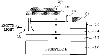
The end face light-emitting thyristor comprises an n-
type semiconductor layer 12, a p-type semiconductor layer 14,
an n-type semiconductor layer 16, and a p-type semiconductor
layer 18 formed on an n-type semiconductor substrate 10; an
anode electrode 20 formed on the p-type semiconductor 18 so
as to make ohmic contact therewith; and a gate electrode 22
formed on the n-type semiconductor layer 16 so as to make
ohmic contact therewith. On the entire structure provided is
an insulting film (not shown) made of a light-transmitting,
insulating material, on which an A1 wiring 24 is further
provided (see Fig.lA). The Al wiring 24 is not shown in
Fig.lB for simplifying the figure. In the insulating film
opened is a contact hole 26 for electrically connecting the
anode electrode 20 to the Al wiring 26. While not shown in
Fig.lB, a cathode electrode is provided on the bottom surface
of the substrate 10.
In this conventional end face light-emitting thyristor,
light is emitted from an end face 23 of the semiconductor
layers 14, 16 both thereof constitute gate layers. As shown
by arrows in Fig.lB, the most of current fed from the anode
electrode 20 flows directly downward (this injected current
is indicated by I1), and a part of the current flows going
round to the gate electrode 22 (this injected current is
indicated by I2). Although both of these injected current I1
CA 02339665 2001-02-06
3
and I2 contribute to light generation in the semiconductor
layers, the light generated by the current I2 cannot
contribute to external light emission from the end face 23
since the current I2 generates light in the area apart from
the end face 23. As a result, the amount of light emitted
from the end face is reduced only by the amount of light not
contributed, thus external light emission efficiency is
decreased.
Disclosure of the Invention
An object of the present invention is to provide an end
face light-emitting thyristor having improved external light
emission efficiency.
Another object of the present invention is to provide a
self-scanning light-emitting element array using such end
face light-emitting thyristor.
According to a first aspect of the present invention, an
end face light-emitting thyristor for emitting light from an
end face thereof comprises a first semiconductor layer of a
first conductivity type, a second semiconductor layer of a
second conductivity type, a third semiconductor layer of the
first conductivity type, and a fourth semiconductor layer of
the second conductivity type stacked in that order on a
substrate of the first conductivity type; an electrode
provided in such a manner that a part thereof makes ohmic
contact with the fourth semiconductor layer in the vicinity
of the end face for injecting current into the semiconductor
layers; and an insulating layer provided between the fourth
semiconductor layer and the part of the electrode that is not
made ohmic contact with the fourth semiconductor layer.
CA 02339665 2001-02-06
4
It is also possible that an opening is formed in the
part of the insulating layer faced to the end face, making
the electrode ohmic contact with the fourth semiconductor
layer via the opening.
In this way, the flow of the current injected from the
electrode is concentrated to near the end face of the light-
emitting thyristor.
According to a second aspect of the present invention,
an end face light-emitting thyristor for emitting light from
an end face thereof comprises a first semiconductor layer of
a first conductivity type, a second semiconductor layer of a
second conductivity type, a third semiconductor layer of the
first conductivity type, and a fourth semiconductor layer of
the second conductivity type stacked in that order on a
substrate of the first conductivity type; a first electrode
provided on the fourth semiconductor layer; and a second
electrode provided on the third semiconductor layer. The
first, second and third semiconductor layers have a necked
portion or a groove between a region including the first
electrode and a region including the second electrode.
By providing such necked portion or groove, the
resistance value between the region including the first
electrode and the region including the second electrode
becomes larger. As a result, the external emission
efficiency is increased because the current component which
flows toward the region including the second electrode is
decreased, thus the most of the injected current flows in the
region including the first electrode.
Using end face light-emitting thyristor described above,
a self-scanning light-emitting element array of the following
CA 02339665 2001-02-06
structure may be implemented.
A first structure of the self-scanning light-emitting
element array comprises a plurality of light-emitting
elements each having a control electrode for controlling
5 threshold voltage or current for light-emitting operation.
The control electrodes of the light-emitting elements are
connected to the control electrode of at least one light-
emitting element located in the vicinity thereof via an
interactive resistor or an electrically unidirectional
element, and a plurality of wiring to which voltage or
current is applied are connected to electrodes for
controlling the light emission of light-emitting elements.
A second structure of the self-scanning light-emitting
element array comprises a self-scanning transfer element
array having such a structure that a plurality of transfer
elements each having a control electrode for controlling
threshold voltage or current for transfer operation are
arranged, the control electrodes of the transfer elements are
connected to the control electrode of at least one transfer
element located in the vicinity thereof via an interactive
resistor or an electrically unidirectional element, power-
supply lines are connected to the transfer elements by
electrical means, and clock lines are connected to the
transfer elements; and a light-emitting element array having
such a structure that a plurality of light-emitting elements
each having a control electrode for controlling threshold
voltage or current are arranged, the control electrodes of
the light-emitting element array are connected to the control
electrodes of said transfer elements by electrical means, and
lines for applying current for light emission of the light-
CA 02339665 2001-02-06
6
emitting element are provided.
According to the structures described above, increased
external emission efficiency, high-densitiy, compact and low
cost self-scanning light-emitting element arrays may be
implemented.
Brief Description of the Drawings
Figs.lA and 1B are diagrams illustrating the structure
of a conventional end face light-emitting thyristor.
Figs.2A and 2B are diagrams illustrating the structure
of an end face light-emitting thyristor in a first embodiment
of the present invention.
Figs.3A and 3B are diagrams illustrating the structure
of an end face light-emitting thyristor in a second
embodiment of the present invention.
Figs.4A and 4B are diagrams illustrating the structure
of an end face light-emitting thyristor in a third embodiment
of the present invention.
Figs.5A and 5B are diagrams illustrating the structure
of an end face light-emitting thyristor in a fourth
embodiment of the present invention.
Fig.6 is an equivalent circuit diagram of a first
structure of a self-scanning light-emitting element array.
Fig.7 is an equivalent circuit diagram of a second
structure of a self-scanning light-emitting element array.
Fig.8 is an equivalent circuit diagram of a third
structure of a self-scanning light-emitting element array.
Best Mode for Carrying Out the Invention
A first embodiment of an end face light-emitting
CA 02339665 2001-02-06
7
thyristor according to the present invention will now be
described. Fig.2A is a plan view of an end face light-
emitting thyristor of the first embodiment, and Fig.2B is a
cross-sectional view taken along the X-Y line in Fig.2A. In
this end face light-emitting thyristor, an n-type
semiconductor layer (a cathode layer) 12, a p-type
semiconductor (a base layer) 14, an n-type semiconductor
layer (a base layer) 16, and a p-type semiconductor layer (an
anode layer) 18 are stacked on an n-type semiconductor
substrate 10. On the anode layer 18 provided is an insulting
film 19 apart from the end face 23. On the insulating film
19 and the part of the anode layer 18 not covered by the
insulating film 19 provided is an anode electrode 20. On the
gate layer 16 provided is a gate electrode 22.
The end face light-emitting thyristor of this embodiment
is different from the conventional thyristor shown in Figs.lA
and 1B only in that the insulating film 19 is further
provided on the anode layer 18. The reason why the
insulating film 19 is provided will be explained in the
following. In order to increase the external emission
efficiency of an end face light-emitting thyristor, it is
required that the anode electrode 20 is to be ohmic contacted
with the anode layer 18 in the vicinity of the end face 13 so
that the flow of the current injected from the anode
electrode 20 is concentrated to near the end face 13. The
size of the anode electrode 20 itself cannot be made small to
concentrate the current to near the end face 13, since the
anode electrode is required to make contact with the A1
wiring as shown in Fig.lA. In this embodiment, consequently,
between the anode 20 and the anode layer 18 provided is the
CA 02339665 2001-02-06
8
insulating film 19 apart from the end face 13 so as to remain
the region where the anode electrode 20 is ohmic contacted to
the anode layer 18 only in the vicinity of the end face 13.
In this case, if the contact area between the anode electrode
20 and the anode layer 18 becomes smaller, then the flow
distribution of the current injected from the anode electrode
20 is narrowed so that the external emission efficiency is
increased. Assuming that the length and width of the contact
area between the anode electrode 20 and the anode layer 18
are L and W, respectively, as shown in Fig.2A, when the case
1 in which L=5,um and W=10,~cm and the case 2 in which L=l0,um
and W=10 ,u m are compared with each other, it is appreciated
that the case 1 having smaller L realizes about 50% larger
amount of light emission than that of the case 2.
A second embodiment of an end face light-emitting
thyristor according to the present invention will now be
described. Fig.3A is a plan view of an end face light-
emitting thyristor of the second embodiment, and Fig.3B is a
cross-sectional view taken along the X-Y line in Fig.3A. It
is noted that elements similar to those in Figs.2A and 2B are
designated by the same reference numeral as in Figs.2A and 2B.
The second embodiment intends to narrow the current flow
distribution in a width direction of the anode electrode in
the first embodiment. For that purpose, an insulating film
30 is provided on the anode layer 18 starting from the end
face 23, and an opening (the width Wo, and the length Lo) 32
is formed in the insulating film at the end face 23. Through
the opening 32, made is a part of the anode electrode 20
ohmic contact with the anode layer 18. It is possible,
therefore, to select the contact area (WoX Lo) of the anode
CA 02339665 2001-02-06
9
electrode 20 to the anode layer 18. According to this
structure, the width Wo of the opening 32 may be smaller than
the width W of the electrode 20, resulting in the substantial
decrease of the contact area of the anode electrode 20 to the
anode layer 18. Therefore, the density of the current
through the semiconductor layers is increased so that the
external emission efficiency may be elevated.
A third embodiment of an end face light-emitting
thyristor according to the present invention will now be
described. Figs.4A and 4B are plan and side views of an end
face light-emitting thyristor according to the third
embodiment. The structure of this embodiment is essentially
the same as that of the thyristor shown in Figs.lA and 1B.
In Figs.4A and 4B, therefore, elements similar to those in
Figs.lA and 1B are designated by the same reference numeral
as in Figs.lA and 1B.
In the end face light-emitting thyristor of this
embodiment, notches 28 are provided on both sides of the
semiconductor layers 12, 14 and 16 between the region 25
including the anode electrode 20 and the region 27 including
the gate electrode 22 to form a necked portion 30 on the
semiconductor layer 12, 14 and 16. The notches 28 can be
easily formed by etching.
Since the width d of the necked portion 30 is smaller
than the width D of the semiconductor layer 12, 14 and 16,
the resistance value of the necked portion 30 becomes larger.
As a result, the current injected from the anode electrode 20
does not flow toward the gate electrode as shown by an arrow
in Fig.4B, thus contributing more to light generation under
the anode electrode. When D=13,u m, and d=5,u m, the external
CA 02339665 2001-02-06
emission efficiency is increased by about 10%.
In order to increase further the external emission
efficiency of the end face light-emitting thyristor, the
contact area between the anode electrode 20 and the anode
5 layer 18 is to be decreased as shown in the first and second
embodiments.
A fourth embodiment of an end face light-emitting
thyristor according to the present invention will now be
described. Figs.5A and 5B are plan and side views of an end
10 face light-emitting thyristor according to the fourth
embodiment. The structure of this embodiment is essentially
the same as that of the thyristor shown in Figs.lA and 1B.
In Figs.5A and 5B, therefore, elements similar to those in
Figs.lA and 1B are designated by the same reference numeral
as in Figs.lA and 1B.
According to the end face light-emitting thyristor of
this embodiment, a groove 32 is provided on the n-type
semiconductor (n-type gate layer) between the region 25
including the anode electrode 20 and the region 27 including
the gate electrode 22. The depth t of the groove 32 is such
that the groove is kept a certain distance away from a
depletion layer formed between the n-type semiconductor layer
16 and the p-type semiconductor layer 14. This is because if
the groove 32 reaches the depletion layer, the resistance
value of the n-type semiconductor layer 16 between the anode
electrode 20 and the gate electrode 22 becomes large,
remarkably aggravating the electrical property of the
thyristor.
By providing the groove 32, the resistance value between
the anode electrode region and the gate electrode becomes
CA 02339665 2001-02-06
11
large. As a result, the current injected from the anode
electrode 20 does not flow toward the gate electrode as shown
by an arrow in Fig.5B, thus contributing to light generation
under the anode electrode. When the thickness T of the n-
type semiconductor layer 16 is l,u m and the depth t of the
groove is 0.5 ,u m, the external emission efficiency is
increased by about 10%.
In order to increase further the external emission
efficiency of the end face light-emitting thyristor, the
contact area between the anode electrode 20 and the anode
layer 18 is to be decreased as shown in the first and second
embodiments.
In embodiments 1, 2, 3 and 4 described above,
semiconductor layers are stacked in the order of npnp on an
n-type semiconductor substrate. Needless to say, this
invention can be applied to a structure where semiconductor
layers are stacked in the order of pnpn on a p-type
semiconductor substrate. In this case, the type of electrode
provided on the uppermost n-type semiconductor layer is a
cathode electrode, while that provided on the rear surface of
the p-type semiconductor substrate is an anode electrode.
The reason why a semiconductor layer of the same
conductivity type as the semiconductor substrate is stacked
immediately above the semiconductor substrate in the above
embodiments is in the following. In general, when a pn (or
np) junction is formed directly on the surface of a
semiconductor substrate, the poor crystallinity of the formed
semiconductor layer tends to degrade the properties of a
device. This is because when a crystal layer is epitaxially
grown on a substrate surface, the crystallinity near the
CA 02339665 2001-02-06
12
substrate is degraded compared with the crystallinity after
the crystal layer has been grown above a certain level. The
above problem can be solved by first forming the same
semiconductor layer as the semiconductor substrate, and then
forming the pn (or np) junction. It is therefore desirable
to interpose the semiconductor layer therebetween.
Three fundamental structures of self-scanning light
emitting element arrays to which the end face light-emitting
thyristor of the present invention can be applied will now be
described.
Fig.6 shows an equivalent circuit diagram of a first
fundamental structure of the self-scanning light-emitting
element array. According to the structure, end face light-
emitting thyristors "' T_2, T_1, To, T+1, T+Z "' are used as
light-emitting elements, each of thyristors comprising gate
electrodes "' G_2, G_1, Go, G+1, G+Z "' , respectively. Supply
voltage V~~ is applied to all of the gate electrodes via a
load resistor RL, respectively. The neighboring gate
electrodes are electrically connected to each other via a
resistor RI to obtain interaction. Each of three transfer
clock (~1, ~z. ~3) lines is connected to the anode electrode
of each light-emitting element at intervals of three elements
(in a repeated manner).
The operation of this self-scanning light-emitting
element array will now be described. Assume that the
transfer clock ~3 is at a high level, and the light-emitting
thyristor To is turned on. At this time, the voltage of the
gate electrode Go is lowered to a level near zero volts due
to the characteristic of the light-emitting thyristor.
Assuming that the supply voltage Vex is 5 volts, the gate
CA 02339665 2001-02-06
13
voltage of each light-emitting thyristor is determined by the
resistor network consisting of the load resistors RL and the
interactive resistors RI. The gate voltage of a thyristor
near the light-emitting thyristor To is lowered most, and the
gate voltage V(G) of each subsequent thyristor rises as it is
remote from the thyristor To. This can be expressed as
follows:
V(Go)~V(G+1)=V(G_i)~V(G+z)=V(G_Z)~........( 1 )
The difference among these voltages can be set by properly
selecting the values of the load resistor RL and the
interactive resistor R=.
It is known that the turn-on voltage VoN of the light-
emitting thyristor is a voltage that is higher than the gate
voltage V(G) by the diffusion potential Vdif of pn junction as
shown in the following formula.
VoN=V(G)+Vdif '~.......(2)
Consequently, by setting the voltage applied to the anode to
a level higher than this turn-on voltage VoN, the light-
emitting thyristor may be turned on.
In the state where the light-emitting thyristor To is
turned on, the next transfer clock ~, is raised to a high
level. Although this transfer clock ~1 is applied to the
light-emitting thyristors T+1 and T_2 simultaneously, only the
light-emitting thyristor T+1 can be turned on by setting the
high-level voltage VH of the transfer clock 1
to the
following range.
V ( G-2 ) +Vdif ~VH ~V ( G+1 ) +Vdif ~ ~ ....... ( 3 )
By doing this, the light-emitting thyristors To and T+1
are turned on simultaneously. When the transfer clock ~3 is
lowered to a low level, the light-emitting thyristors To is
CA 02339665 2001-02-06
14
turned off, and this completes transferring ON state from the
thyristor To to the thyristor T+1
Based on the principle described above, the ON state of
the light-emitting thyristor is sequentially transferred by
setting the high-level voltage of the transfer clocks ~1, ~
and ~ 3 in such a manner as to overlap sequentially and
slightly with each other. In this way, the self-scanning
light-emitting array according to the present invention is
accomplished.
Fig.7 shows an equivalent circuit diagram of a second
fundamental structure of the self-scanning light-emitting
element array. This self-scanning light-emitting element
array uses a diode as means for electrically connecting the
gate electrodes of light-emitting thyristors to each other.
That is, the diodes ~~~ D_Z, D_1, Do, D+1 ~~~ are used in replace
of the interactive resistors R1 in Fig.6. The number of
transfer clock lines may be only two due to the
unidirectional of diode characteristics, then each of two
clock (~1 ,~z ) lines is connected to the anode electrode of
each light-emitting element at intervals of two elements.
The operation of this self-scanning light-emitting
element array will now be described. Assume that as the
transfer clock ~ 2 is raised to a high level, the light-
emitting thyristor To is turned on. At this time, the
voltage of the gate electrode Go is reduced to a level near
zero volts due to the characteristic of the thyristor.
Assuming that the supply voltage v~R is 5 volts, the gate
voltage of each light-emitting thyristor is determined by the
network consisting of the load resistors RL and the diodes D.
The gate voltage of an thyristor nearest to the light-
i
CA 02339665 2001-02-06
emitting thyristor To drops most, and the gate voltages of
those thyristors rise as they are further away from the
light-emitting thyristor To.
The voltage reducing effect works only in the rightward
5 direction from the light-emitting thyristor To due to the
unidirectionality and asymmetry of diode characteristics.
That is, the gate electrode G+1 is set at a higher voltage
with respect to the gate electrode Go by a forward rise
voltage Vdif of the diode, while the gate electrode G+2 is set
10 at a higher voltage with respect to the gate electrode G,1 by
a forward rise voltage Vdif of the diode. On the other hand,
current does not flow in the diode D_1 on the left side of
the light-emitting thyristor To because the diode D_1 is
reverse-viased. As a result, the gate electrode G_1 is at
15 the same potential as the supply voltage VCR.
Although the next transfer clock ~1 is applied to the
nearest light-emitting thyristor T.,1, T_l; T+3, T_3; and so on,
the thyristor having the lowest turn-on voltage among them is
T+1, whose turn-on voltage is approximately the gate voltage
2 0 of G,.1 + Vdif i about twice as high as Vdif ~ The thyristor
having the second lowest turn-on voltage is T+3, about four
times as high as Vdif~ The turn-on voltage of the thyristors
T_1 and T_3 is about Vex + Vdif
It follows from the above discussion that by setting the
high-level voltage of the transfer clock ~1 to a level about
twice to four times as high as Vdif, only the light-emitting
thyristor T+1 can be turned-on to perform a transfer
operation.
Fig.8 shows an equivalent circuit diagram of a third
fundamental structure of the self-scanning light-emitting
CA 02339665 2001-02-06
16
element array. According to the structure, a transfer
portion 40 and a light-emitting portion 42 are separated.
The circuit structure of the transfer portion 40 is the same
as that shown in Fig.7, and the light-emitting thyristors ~~~
T_1, To, T+1, T+Z ~~~ are used as transfer elements in this
embodiment.
The light-emitting portion 42 comprises writable light-
emitting elements L_1, Lo, L+1, L+Z ~~~ . each gate thereof is
connected to the gate ~~~G_1, Go, G+1~~~ of the transfer elements
~~~T_1, To, T+1, T+z. respectively. A write signal Sin is applied
to all of the anode of the writable light-emitting elements.
In the following, the operation of this self-scanning
light-emitting array will be described. Assuming that the
transfer element To is in the ON state, the voltage of the
gate electrode Go lowers below the supply voltage v~R and to
almost zero volts. Consequently, if the voltage of the
write signal Sin is higher than the diffusion potential
(about 1 volt) of the pn junction, the light-emitting element
Lo can be turned into a light-emission state.
On the other hand, the voltage of the gate electrode G_1
is about 5 volts, and the voltage of the gate electrode G+1
is about 1 volt. Consequently, the write voltage of the
light-emitting element L_1 is about 6 volts, and the write
voltage of the light-emitting element L+1 is about 2 volts.
It follows from this that the voltage of the write signal
which can write only in the light-emitting element La is a
range of about 1-2 volts. When the light-emitting element
Lo is turned on, that is, in the light-emitting state, the
voltage of the write signal Sin is~fixed to about 1 volt.
Thus, an error of selecting other light-elements can be
CA 02339665 2001-02-06
17
prevented.
Light emission intensity is determined by the amount of
current fed to the write s ignal Sin, an image can be written
at any desired intensity. In order to transfer the light
s emitting state to the next element, it is necessary to first
turn off the element that is emitting light by temporarily
reducing the voltage of the write signal Sin down to zero
volts.
Industrial Applicability
This invention makes it possible to provide an end face
light-emitting thyristor having good external light emission
efficiency. A self-scanning light-emitting element array
using this end face light-emitting thyristor has improved
external light emission efficiency and require no driving
circuit, thus achieving a low-cost optical print head for
optical printers. When the self-scanning light-emitting
element array using this end face light-emitting thyristor is
applied to optical print heads, high-quality printing can be
accomplished because each light-emitting element has improved
external light emission efficiency.