Note: Descriptions are shown in the official language in which they were submitted.
CA 02339745 2001-03-02
-1-
METHOD AND APPARATUS FOR MrANUFACTURING
PHOTONIC CRYSTAL ELEMENT
BACKGROUND OF THE INVENTION
The present invention relates to a method and apparatus for the
manufacture of a photonic crystal element.
The photonic crystal element is an artificial crystal in which two kinds
of media of vastly different refractive indices (dielectric constants) are
arranged regularly with a period of the order of li~:ght wavelength.
Conventionally, the photonic crystal element of such a structure is
manufactured using an apparatus of such a construction as depicted in Fig. 1.
The apparatus of Fig. 1 is designed to orient dielectric fine particles 13
two or three-dimensionally in a container 12 placed on an XY stage 11. A
spray source 15 is driven and controlled so that fiine particles 13 contained
in
a powder container 14 are jetted out, for example, one by one from a jet
nozzle 16, while at the same time the XY stage l :l is driven to orient the
fine
particles 13 in a desired pattern.
In this example, the jet nozzle 15 is mounted on a Z stage 17 in a
manner to be movable in a Z direction (in the vertical direction). Reference
numeral 18 denotes a DC servomotor for driving the Z stage 17. The spray
source 15, the DC servomotor 18 and a DC servomotor (not shown) for
driving the XY stage 11 are driven and controlled. by a controller 19.
With the conventional photonic crystal element manufacturing method
using the above-described apparatus, it is necessary, for the emergence of a
photonic band gap in the light wavelength band, to arrange the fine particles
on the order of light wavelength (submicron to several microns); that is, the
jet of the fine particles and the XY stage need to t>e controlled with such an
CA 02339745 2004-10-25
-2-
extremely high degree of accuracy.
Since such control presents serious difficulties, however, the
manufacture of the photonic crystal element is not easy; in particular, much
difficulties are encountered in manufacturing the photonic crystal element as
S intended.
In U.S. Patent No. 5,651,818 there is disclosed a method of
preparation of a photonic crystal element from a composite material.
According to this conventional method, the photonic crystal element is
fabricated by impregnating a reticulated mesh formed in a metal column of a
high-melting point such as tungsten (W), by capillary action, with liquid
material of a melting point lower than that of the metal column, such as
aluminum oxide, and dissolving the metal column after the liquid material
solidifies. With this method, however, it is difficult to form the photonic
crystal element with reticulated mesh spacing held uniform in the entire body
of the photonic crystal element on the order of light wavelength.
SL)1'vIMARY OF THE INVENTION
It is therefore an object of the present invention to provide a method
that permits easy orientation of fine particles and hence facilitates the
manufacture of photonic crystal elements, and an apparatus that implements
the method.
The photonic crystal element manufacturing method according to the
present invention comprises the steps of: (a) orienting and dispersing fine
particles in a liquid polymer contained in a container; (b) obtaining from the
liquid polymer a solid composite material in which the fine particles are
oriented and dispersed such that a photonic band gap cannot emerge; and (c)
performing high-density compression molding of said composite material to
compress said solid composite material into a compressed size in which the
CA 02339745 2004-10-25
-3-
fine particles are dispersed such that the photonic band gap emerges, thereby
obtaining a photonic crystal element.
In the above method, the high-density compression molding of the
composite material is carried out by isostatic press through a pressure
medium.
In the above method, the composite material is heated at the time of its
high-density compression molding.
In the method, the fine particles are magnetic fine particles and an
electromagnetic field is applied to the composite material at either one or
both
of the times of orientation and dispersion or high-density compression
molding.
The present invention further provides a photonic crystal element
manufacturing method comprising the steps of (a) orienting and dispersing
fine particles in a polymer medium which is contained in a container; (b)
solidifying the polymer medium within the container to obtain a solid
composite material in which the fine particles are dispersed in such a scale
that a photonic band gap does not emerge; and (c) applying high-density
isostatic compression molding to said solid composite material to compress
the composite material into a compressed size in which the fine particles
dispersed therein are compressed in such a compressed scale that a photonic
band gap emerges, thereby obtaining a photonic crystal element.
The apparatus according to the present invention for manufacturing a
photonic crystal element from a composite material with magnetic fine
particles oriented and dispersed in a polymer medium, comprises: means for
applying an isostatic pressure to said composite material; means for heating
said composite material; and means for applying an electromagnetic field to
said composite material.
CA 02339745 2003-10-29
-3 a-
BRIEF DESCRIPTION OF THE DRAWINGS
Fig. 1 is a schematic diagram for explaining a conventional photonic
crystal element manufacturing method;
Fig. 2 is a schematic diagram for explaining an embodiment of the
photonic crystal element manufacturing method according to the present
invention; and
Fig. 3 is a schematic diagram illustrating an embodiment of the
photonic crystal element manufacturing apparatus according to the present
invention.
DETAILED DESCRIPTION OF THE PREFERRED EMBODIMENTS
Fig. 2 schematically illustrates a sequence of steps involved in the
CA 02339745 2001-03-02
-4-
manufacture of the photonic crystal element according to an embodiment of
the present invention. The manufacturing step:. (a) to (g) will be described
below in due order.
Step (a): A liquid polymer 22 is poured a;> a medium into a container
21, and fine particles 23 are oriented and dispersed in the liquid polymer 22.
The fine particles 23 are spaced apart, for example, tens of micrometers (~.m)
to several millimeters (mm).
Step (b): The liquid polymer 22 in the container 21 is set by heating
with an electric furnace or the like (not shown).
Step (c): A solid composite material 24 is obtained by the heat-setting
of the liquid polymer 22. The composite material 24 by steps (a) and (b) can
be obtained using a known method.
Step (d): The composite material 24 is taken out of the container 21
and hermetically sealed in a plastic bag or similar sealing envelope 25.
Step (e): Isostatic pressure is applied to the hermetically sealed
composite material 24.
Step (f): The composite material 24 undergoes high-density
compression molding by the isostatic pressing while holding the orientation
of the fine particles 23 unchanged. At this time the photonic band gap
emerges by compressing the composite material 24 to such an extent that the
spacing of the fine particles 23 becomes of the order of submicron.
Step (g): Finally, the sealing envelope 25 its removed, with which the
manufacture of a photonic crystal element 26 is completed.
As described above, this embodiment user the conventional composite
material producing method such as disclosed, for example, in I. Kaetsu et al,
J.
Polymer SCi, A-1 10 2203(1972), p.l 18, and ca.rr:ies out the orientation of
the
fine particles 23 in the liquid polymer 22 on a lar~;e scale (tens of
micrometers
CA 02339745 2001-03-02
-S-
to several millimeters) where manipulations are easy. And the composite
material 24 thus obtained is compressed at a stroke into a high-density
molding of such a size that the photonic band gap develops; in this way, the
photonic crystal element 26 is manufactured.
The sealing envelope 25 for hermetically sealing the composite
material 24 is not limited specifically to the plastic bag but may be a rubber
bag or glass capsule as well. The material for the fine particles 23 is
alumina
or silicon in this embodiment.
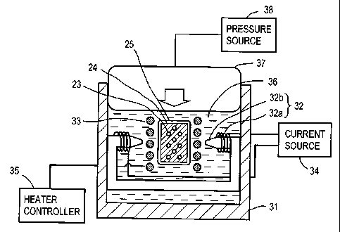
Fig. 3 is a schematic showing of an embodiment of the photonic
crystal element manufacturing apparatus according to the present invention.
This apparatus is suited to producing the photonic crystal element from the
composite material 24 made using the fine particles 23 of ferrite or similar
magnetic material.
In a cylinder 31 there are placed a pair of opposed electromagnets 32
and a coiled heater 33 as shown. A current source 34 is to supply current to
coils 32a of the electromagnets 32, and energizat:ion of the heater 33 is
controlled by a heater controller 35.
The cylinder 31 is filled with a pressure medium 36, wherein the
composite material 24 hermetically sealed in the ;>ealing envelope 25 is
placed
in a gap defined by the heater 33 with yokes 32b of the electromagnets 32
disposed opposite each other.
The pressure medium 36 may be water, oil, or gas such as argon (Ar)
or N2.
A piston 37 engaged with the cylinder 31 :is driven by a pressure
source 38 to pressurize the pressure medium 36, thereby applying the isostatic
pressure to the composite material 24.
With this apparatus, it is possible to apply the isostatic pressure and an
CA 02339745 2001-03-02
-6-
electromagnetic field to the composite material ;?4 by the electromagnets 32
and heat it by the heater 33.
Accordingly, it is feasible to achieve high-density compression
molding of the composite material 24 by HIP (Hot Isostatic Press) while at the
same time controlling the orientation of the fine particles 23 by applying a
high-intensity electromagnetic field to the composite material 24. Hence,
the photonic crystal element 26 can easily be manufactured as desired. In
the case of heating the composite material 24 by the heater 33; a medium
other than water is used as the pressure medium .36.
With the use of the manufacturing apparatus of Fig. 3, the orientation
of the magnetic fine particles can be controlled by the application of an
electromagnetic field to the composite material 24 during its high-density
compression molding. The orientation control i:or the fine particles
(magnetic fine particles) by the application of an electromagnetic field may
also be effected at the same time as the composite material 24 is produced,
that is, as the fine particles 23 are oriented and dispersed in the polymer
medium, or both during the orientation and dispersion of the fine particles 23
and during the high-density compression molding of the composite material
24.
EFFECT OF THE INVENTION
As described above, according to the manufacturing method of the
present invention, the composite material in which fine particles are oriented
is high-density compression-molded, by which the fine particle spacing is
reduced to develop the photonic band gap necessary for the photonic crystal
element. Since the orientation of the fine particles is carried out on the
scale
where the required manipulations are easy to perform, allowing ease in
CA 02339745 2001-03-02
-7-
manufacturing the photonic crystal element.
Further, this invention method permits se~tisfactory high-density
compression molding of the composite material by the isostatic press scheme
through the pressure medium and achieves control of the orientation of the
fine particles by the application of an electromagnetic field during their
orientation and dispersion in the pressure medium, thus ensuring a higher
level of satisfaction in manufacturing the desired photonic crystal element.
Moreover, the manufacturing apparatus according to the present
invention allows application of an isostatic pressure, heat and an
electromagnetic field to the composite material in which magnetic fine
particles are oriented, and hence the orientation of the fine particles can be
controlled--this facilitates the manufacture of the. desired photonic crystal
element.
It will be apparent that many modifications and variations may be
effected without departing from the scope of the novel concepts of the present
invention.
25