Note: Descriptions are shown in the official language in which they were submitted.
CA 02341048 2001-03-15
NOVEL OPTICAL WAVEGUTDE SWITCH USING CASCADED MACH-
ZEHNDER INTERFEROMETERS
BACIS;GROUND OF THE INVENTION
Field of the Invention
The present invention relates to optical waveguide switches in general and in
particular to
1o switches utilizing double-track cascaded Mach Zehnder interferometers. It
provides
optical switches with high isolation for optical communication systems,
optical
interconnects, optical cross-connects, and large-scale fiber-optic network
systems.
Relevant Art
The rapid development and applications of fiber-optic telecommunication
systems
require new microstructure optoelectronic technologies rather than individual
mechanical
devices. Among such optoelec;tronic technologies, integrated optics represents
a
promising strategy. One impi~ementation of this strategy relies on the
integration of
20 optoelectronic interconnects can a host Silicon (Si) substrate, and thus
requires Si-based
photonic devices. Thermo-optic (T(~) waveguide devices using PECVD-based
silica-on-
silicon have shown an advantage over currently used mechanical and bulk optic
devices
in fiber-optic telecommunications because of their flexibility in fabrication
and
processing, as well as speed o:f operation compared to mechanical ones.
Electro-optic
(E0) waveguide devices using diffused LiNb03-based waveguides also provide
promising applications in the future due to their high-speed operation, low
loss and
mature manufacturing technology. Among active devices in optical communication
l
CA 02341048 2001-03-15
systems, optical space switches are key components. For example, a 2x2 or 1x2
switch is
not only used directly in various optical switching systems as a single
device, but also as
a primitive for building various large-scale switching devices. Beyond the
traditional
applications, optical switches play an increasingly critical role in emerging
mufti-channel
and re-configurable photonic :networks such as the dense wavelength division
multiplexing (DWDM) which is gaining impartance in fiber-optic
telecommunication
systems. Some typical and irr~portant components such as optical multiplexers
(MLTX),
optical demultiplexers (DEMTJX), 2x2 optical switches, and variable optical
attenuators
are used to build configurable optical add/drop multiplexing (C-OADM) systems.
This is
to a typical and popular application of 2x2 optical switches (OS) in DWDM
systems.
Most of the optical switches in production today use opto-mechanical means to
implement optical steering. Tlus is accomplished through the separation, or
the
alignment, or the reflection of the light beam by an opto-mechanically driven
mirror.
Such designs offer good optical performance, but have two main drawbacks. One
is slow
speed, the typical settling timfa for switching being from I O ms to 100 ms.
The other
drawback includes noise and size. In an era when the use of electronics is
considered an
intrusion in the all-optical networks, mechanically based devices are out of
place. To
overcome some of these limitations, non-mechanical and no-moving-part optical
switches
2o in the market now use a variety of design concepts. Both EO and TO
waveguide switches
not only improve operational speed compared to opto-mechanical switches, but
also
make integrated optic circuits possible. In telecommunication systems, optical
networks
are growing at a significant rate. This =growth is driven by the demand for
Internet
2
CA 02341048 2001-03-15
services. As bandwidth demand continues to grow, new network technologies are
rewired to support bandwidth capacities. Optical cross-connects (OXCS)
represents a
new category of network elements which promise to reduce networking equipment
and
operational costs for these high perfarmance bandwidth networks.
There are two kinds of waveguide optical switches: one uses Mach-Zehnder
interferometer (MZI) configurations and the other is a digital optical switch
(DOS). The
former can be either eleetro-optical switch (EOS) based on high EO effect
materials such
as LiNb03 and polymers, or thermo-optical switch (TOS) based on high TO effect
to materials such as polymers and silica. The DOS may only be TOS based due to
currently
available EO effect materials. The TOS using MZI configurations has an
advantage of
low power consumption, but the disadvantage of low reliability due to
interference. The
TOS based DOS configuration has the disadvantage of high power consumption,
but the
advantage of high reliability, because it is based on digital cut-off of the
optical path.
Therefore, the TOS based MZI configuration is suitable for both high and low
thermal
coefficient (dn/dT) if the material is reliable and stable both in time and
temperature such
as PEC~D-based silica-on-siii:con. The MZI configuration (based on waveguide
technology) has two arms: one; arm is heated to create an optical path-length
difference
with respect to the other arm. 'Thus, the output optical power depends on the
temperature
2o difference between the two paths. Several companies produce this type of
device.
3
CA 02341048 2001-03-15
SUlwIMARY OF THE INVENTION
In a preferred implementation, the present invention provides an optical
waveguide
switch using four Mach-Zehnder interferometer (MZI) units. These four MZI
units are
arranged as a 2x2 matrix to form a double-track 2-cascaded MZI configuration,
which
increases the isolation between the outputs and the extinction ratio at each
output port.
Two outputs from each MZI in the first column are separately connected to
inputs of the
other two MZI units in the sec-and column. In the first column of MZIs, one
input port of
each MZI is used as input port: and the other one as an idle port (not used).
Likewise, in
I o the second column of MZIs , one output port of each MZI is used as an
output port and
the other one as an idle port. Hence, an optical signal at the matrix input
must pass
through two MZI units, in contrast to the conventional 2x2 waveguide switches
based on
a single MZI unit, where an optical signal passes through a single MZI unit
and isolation
of more than 20dB is difficult to achieve because of processing errors in
making the
waveguides. The extinction ratio is also limited by the isolation, since an
optical signal
through the present matrix ha<.; to pass through two MZI units in any event,
given
interference effects in two M:~;I units, the isolation of the present 2x2
optical switch can
be twice as large as the conventional 2x2 optical switch based on a single MZI
unit.
2o One modulating electrode is used for each MZI unit to change the optical
phase by ~.
Every two electrodes in the same row of the MZI matrix are interconnected as
one
electrode to cause the optical signals launched into the input port of the
same row of the
MZI matrix to experience two Mach-Zehnder interfering effects. The extinction
ratio is
4
i a
CA 02341048 2001-03-15
also doubled. Because the 2x:? switch based on the current invention uses more
MZI
units and the corresponding electrodes, it has more functians for any input
optical signal
than the conventional 2x2 optiical switch based on a single MZI unit. The
modulating
form can be either the TO or the EO.
The 2x2 switch may be simplified to provide a 1x2 switch by omitting one row
of the
MZI matrix. An MxN switching matrix may be implemented using more than two of
the
present 2x2 waveguide switching matrix.
1o BRIEF DESCRIPTION OF THE DRAWINGS
The preferred exemplary embodiments of the present invention will now be
described in
detail in conjunction with the annexed drawing, in which:
Figures 1 (a), 1 (e), 1 (c) and 1 (d) illustrate the configuration of a 2x2
waveguide switch
according to the present invention using the double-track 2-cascaded Mach-
Zehnder
interferometers and the preferred connections of control electrodes, where
FIG. 1(a) is a
top view, FIG. 1(b) is a cross-section along the axis A-A, FIG 1(c) shows the
control
electrodes connected in parallel and FIG. 1(d) shows the control electrodes
connected in
20 series;
Figure 2 illustrates the configuration of a 1x2 waveguide switch using a
single-track 2-
cascaded Mach-Zehnder interferometers, where FIG. 2(a) is a top view and FIG.
2(b) is a
cross section along the axis B-B;
CA 02341048 2001-03-15
Figure 3 illustrates an alternative cross-section along the axis A-A of the
2x2 waveguide
switch Shawn in Figures l(a) and I(b) based on vertical EO modulation, using
two
control electrodes for each waveguide; and
Figures 4(a) and 4{b) illustrate; a configuration of a 2x2 waveguide switch
using the
double-track 2-cascaded Mach-Zehnder interferometers based on two electrodes
for each
waveguide, co-planar EO modlulation where FIG-4(a) is a top view and FIG. 4{b)
is a
cross-section along the axis C-C.
DETAILED DESCRIIPTION OF THE PREFERRED EMBODIMENTS
A waveguide switch based on the Mach-Zehnder interferometer (MZI)
configuration has
two 3dB directional couplers connected by two waveguide arms. The switch
exploits the
phase property of light. The input light is split by one coupler and sent to
two separate
waveguide arms, then recombined and split again by the second coupler. One or
both
waveguide arms are modulated to produce a difference in optical path length
between the
two waveguide arms. The modulating means can be either thermo-optic (TO) or
electro-
optic (E0). If the two optical paths are the same length, light chooses one
output of the
2o second coupler, if they have a phase difference of ~ it chooses the other
output port. As a
2x2 switch, for an input optical signal, the isolation between two output
ports is important
because it directly determines the ON/OFF extinction ratio of an output port.
Meanwhile,
the isolation is strangiy dependent on the coupling ratio of the two 3dB
directional
couplers. Namely, the closer the ratio is to 50% the higher is the isolation
of the 2x2
6
i r
CA 02341048 2001-03-15
switch, and the higher is the C~N/OFF extinction ratio at each output port. In
theory, if the
coupling ratio of the 3dB cougrler is exactly 50% (i.e., -3dB), the isolation
between the
two output ports should be infinity. In fact, no perfect 3dB directional
coupler exists,
because errors in both design and fabrication, especially in fabrication, are
not avoidable.
So, it is difficult for 2x2 waveguide switches based on a single MZI unit to
achieve an
isolation of 20dB. In practical fiber-optic communications, not only is an
isolation of
more than 20 dB often required for switching systems, but also isolation of
more than 30
dB is necessary for some DWI~M networks, such as typical optical add/drop
multiplexing
systems.
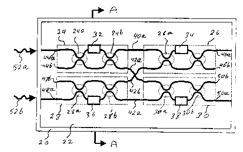
Referring now to FIGS. 1 (a) and 1 (b), the waveguide switch of the present
invention
comprises a substrate 20, cladding 22 and four waveguide MZI units 24, 26, 28
and 30
and four modulating electrodes 32, 34, 36 and 38 (they are also called heaters
for thermal
modal tion). The MZI unit 24 comprises two 3dB directional couplers 24a and
24b. The
MZI unit 26 comprises two 3fB directional couplers 26a and 26b. The MZI 28
comprises
two 3dB directional couplers 28a and 28b. The MZI unit 30 comprises two 3dB
directional couplers 30a and 30b. The four modulating electrodes 32, 34, 36
and 38 are
used on the MZI units 24, 26, 28 and 30, respectively, to modulate the optical
phase of
one optical path of each MZI unit. Each MZI unit has two input ends and hvo
output
2o ends. One output end of the MZI unit 24 is directly connected to the tandem
MZI unit 26
by waveguide path 40a and the other one is cross-connected to the MZI unit 30
by
waveguide path 40b. In the sane manner, one output end of the MZI unit 28 is
directly
connected to the tandem MZI unit 30 by waveguide path 42a and the other one is
cross-
l t
CA 02341048 2001-03-15
connected to the MZI unit 26 lby waveguide path 42b. So, the waveguide paths
40b and
42b have an intersection at 90° and do not interfere with each other.
One input end 44a of
the MZI unit 24 is used as an input port of the 2x2 switch for an optical
signal 52a, and
the other input end 44b is in idle state i.e. remains unconnected. Similarly,
one output end
46a of the MZI unit 26 is used as an output port of the 2x2 switch and the
other output
end 46b is in idle state. In the same manner, one input end 48a of the MZI
unit 28 is ',
used as an input port of the 2x2 switch for an optical input signal 52b and
the other input
end 48b is in idle state. Similarly, one output end 5fla of the MZI unit 30 is
used as an
output port of the 2x2 switch and the other output end SOb is in idle state.
These two idle-
to state output ends are designed to receive the optical noise or the
unexpected optical
signals. In fact, an input optical signal now experiences twice the MZI
effects, such that
isolation between the two output ports 46a and Sfla is doubled.
For simplicity, the TOS is taken as an example to describe the operation and
the
difference between the 2x2 optical switch based on the present invention and
the
conventional 2x2 optical switch using a single MZI configuration. Unlike the
2x2 switch
using a single MZI configuration, where only one electrode is required to
operate the
optical signals launched from any input port, as shown in Fig. l, the present
2x2 switch
uses faun electrodes, where thc~ two electrodes 32 and 34 are required to
switch optical
2o signals launched into input port 44a and the two electrodes 36 and 38 are
required to
switch the optical signals launched from input port 48a. As shown in Fig. l,
the two
electrodes deposited on the saame track are used to operate the optical
signals launched
into this track. If an optical sigmal 52a is launched into the input port 44a,
it is split into
s
l E
CA 02341048 2001-03-15
'~ <
two parts at 50% coupling ratio by the 3dB directional coupler 24a and then
recombined
into one optical signal again by the 3dB directional coupler 24b. If the
electrode 32 is not
activated (i.e., heated for a TOS) by a modulating signal (in the OFF-state),
the optical
signal 52a is sent into the waveguide path 40b as an input optical signal to
the MZI unit
30. This input optical signal is further split into two parts at 50% coupling
ratio by the
3dB directional coupler 30a, and then recombined into one optical signal by
the 3dB
directional coupler 30b. If the electrode 38 is not activated by a modulating
signal {in the
OFF-state), the combined optical signal exits at the output port 50a of the
MZI unit 30,
which is one of the two output: ports of the 2x2 switch. For the same optical
signal 52a
launched into the 3dB directional coupler 24a, when the electrode 32 is
activated by a
modulating signal (in the ON-state), this optical signal exits at the
waveguide path 40a as
an input optical signal to the 1V1ZI unit 2b. So, it is further split into two
parts and sent to
two arms at 50% coupling ratio by the 3dB directional coupler 26a and
recombined into
one optical signal again by the- 3dB directional coupler 2Gb. If the electrode
34 is also
activated, this optical signal e:~its at the output end 46a of the 3dB
directional coupler
26b. As mentioned above, the end 46a is one of the two output ports of the 2x2
waveguide switch. Thus, the optical signal 52a launched into the input port
44a can have
two possible outputs 50a or 4fia by not activating both electrodes 32 and 34
{both in the
OFF-state), or activating both electrodes 32 and 34 (bath in the ON-state),
respectively
2o Thus, switching of the input signal 52a is accomplished. The same switching
process is
also performed if an optical signal 52b is launched into the input port 48a of
the MZI unit
28 by not activating both electrodes 36 and 38 {in the OFF-state), or by
activating both
electrodes 36 and 38 (in the ON-state). Hence, the 2x2 switching process is
implemented
9
l s
CA 02341048 2001-03-15
with the present double-track 2-cascaded MZI configuration. Of course, the two
electrodes 32 and 34 must be operated simultaneously and used as one
modulating
electrode to switch the optical signals such as 52a launched into the input
port 44a of the
2x2 switch, The same applies for the electrodes 36 and 38 to switch the
optical signals
such as 52b launched into the input port 48a of the 2x2 switch. Two electrode
interconnection methods may be used: in parallel or in series as shown in
Figs. l(c) and
Fig. 1 (d), respectively.
Referring now to Figs. 2(a) and 2(b), a 1x2 optical switch may be realized.
The present
2x2 optical switch using eight 3dB directional couplers may be simplified to
yield a 1x2
optical switch using four 3dB directional couplers as shown. The four 3dB
directional
cauplers are 24a, 24b, 26a and 26b are used to form a single-track 2-cascaded
MZI
configuration and two electrodes 32 and 34 are used to modulate the two MZI
units 24
and 26. The isolation for the 1x2 optical switch should be approximately the
same as that
for the 2x2 switch as described above.
Because the present 2x2 switch uses more 1VIZI unites and the corresponding
number of
electrodes, it provides more functions for any input optical signal than the
conventional
2x2 optical switch based on a single MZI unit. For example, an optical signal
52a will
2o have of no output when both the electrodes 32 and 34 are not activated
while at the same
time both the electrodes 36 and 38 are activated. The same applies to the
optical signal
52b when both the electrodes 36 and 38 are not activated while at the same
time both the
electrodes 32 and 34 are activated. Even when the two optical signals 52a and
SZb are
to
l t
CA 02341048 2001-03-15
input into 44a and 48a, respectively, at the same time, the 2x2 optical switch
still
provides this additional function just described.
Referring now to Fig. 3, it shows a cross-section in the plane A-A
{corresponding to that
in Fig. 1{a)) for an EOS, where the top view of such an electro-optically
modulated
switch is identical to that shown in Fig. 1{a). For electro-optical modulation
of the
waveguide it is necessary to provide two electrodes across which a potential
difference is
applied. Therefore, the top electrode, 32 and 36 in Fig. 3 have bottom
counterpass
electrodes 32a and 3Ga, with the modulating electrical signal applying a
potential
to difference between 32135 and 32a/36a in order to create a refractive index
modulating
field between {32 and 32a) and (3G and 36aj, thus inducing the requisite phase
shift in the
waveguides in between.
Figs. 4(a) and 4(b) show an allternative arrangement to that of Fig.3, wherein
the electro-
optical modulating electrodes are deposited on the top surface on ether side
of a
waveguide. The modulating potential difference is thus applied between
electrodes (S4
and 54a) and (S6 and S6a). Of course, structure and operation of the electro-
optically
controlled 1x2 or 2x2 switches is identical to the TOS switches in all other
respects.
2o As mentioned abave, the directional couplers with a coupling ratio of 50%,
known as
3dB directional coupler, are the most useful optical function elements in the
2x2 optical
switch based of the present invention. As shown in Fig. i{a), four MZI units
are formed
with eight 3d8 directional couplers. Each MZI unit consists of two 3dB
directional
m
CA 02341048 2001-03-15
couplers and two waveguide arms of the same length. One of the waveguide arms
has
deposited thereon a metal electrode (which is tailed a heater for thermal
modulation,
while for electrical modulation, two electrodes must be used to replace one
heater
electrode).
Because an optical signal passes through two MZI units no matter which optical
path is
selected, the optical characterxatics of the switch, such as the isolation
between the two
outputs, the switching extinction ratio, the wavelength dependence and the
optical
propagation loss across the device are approximately twice that of a single
MZI unit. The
to following analysis considers one MZI unit. For a 3dB directional coupler,
if the input
optical power is Po and the output powers of the 3dB directianai coupler are P
and Pz at
the bar-state port and the cross-state port, respectively, the coupling ratio
k and the
coupling Loss L~ of the 3dB directional coupler are defined by
k = P PzP Vila)
1 2
L~ =101ogio~P PoP ) (1b)
z
Assuming the change of the refractive index of the waveguide produced by the
modulation is ~e , the phase difference between two waveguide arms of the MZI
unit
2o should be
12
l a
CA 02341048 2001-03-15
~~ _ 2~L~e (
where L is the length of the modulated waveguide {i.e., the length of the
electrode) and
~, is wavelength in vacuum. For the TO modulation, ~c is related to the
temperature
change OT by the TO coefficiient dnldT of the waveguide material as
~ - do ~~,
dT
For the EO modulation, ~ is related to the applied electrical field E by the
EO
coefficient X33 of the waveguide rnateriai as
to ~=-2 r h3E
where n is the refractive inde;~ of the EO waveguide material. Then the two
output
efficiencies of one MZI unit are
~h (1) _ {l - ~k)Z cos2 ( ~~ ) + sine ( ~~ )
(3 )
~7z (1) = 4k(1- k) cost ( ~~ ) {3b)
where r~, {l) and r~2 (1) are the output efficiencies {i.e., the normalized
output power) at
the bar-state output port and the cross-state output port, respectively, and
~~ is the
13
l r
CA 02341048 2001-03-15
o tical hase chan a induced b the modulation. When 0 = ~ On = ~
p p g y ~ ( 2~ ,) a switch
based on single IVIZI unit can produce a switching process, and ~~ _ ~ is the
off state. In
the off state, the refractive index change ~ is 0 and Eqs. (3a) and (3b) can
be written as
y (I) _ (I - 2k)2 , and (4a)
r~2 (I) = 4k(1- k) . (4b)
Thus, the isolation between two output ports of the single MZI unit (i.e., the
isolation of
to the conventional 2x2 optical switch) should be
Iso-MZI =lOlogio(~a(I)). (5)
n~ (1)
In the 2x2 optical switch based on the present invention, because any optical
signal has to
pass through two MZI units, the two output efficiencies at two output ports of
the 2x2
optical switch should be
r~i(2) = r~l (1), and (6a)
rlz(2) _ ~?i (I) ~ (6b)
14
16
CA 02341048 2001-03-15
Thus the isolation between two output ports of the present 2x2 optical switch
should be
defined by
Iso_switch = lOlog,o[ ~1~2}]. (~)
Hence, the following advantages expression is obtained
Iso switch = 2"Iso MZI .
1o The extinction ratio at any output port (the bar-state port or the cross-
state port) is also
increased to twice that of the; conventional 2x2 optical switch.
15