Note: Descriptions are shown in the official language in which they were submitted.
CA 02341110 2001-03-16
1
AVALANCHE PHOTODIODE
FIELD OF THE INVENTION
The present invention relates to an avalanche photodiode that realizes high
sensitivity, low noise, broad band, and low dark current at the same time.
BACKGROUND OF THE INVENTION
The so-called superlattic;e avalanche photodiode (to be referred to
hereinafter
as an APD) that uses a superlattice for the multiplication layer has been used
in
recent years as an APD for optical communications in a wavelength of 1.3 pm or
1.55 p,m. In general, multiplication noise of the APD decreases as a ratio
between ionization rates of electrons and holes (a and (3), which is inherent
to a
semiconductor used for the multiplication layer, departs from value "1". A
superlattice structure is used for the multiplication layer in order to
increase the
ratio of the ionization rates a/~3 or ~i/a. It has been known that, an Ino.s,
Alo.as ~ /
Ino.s Gao ~ ~o.~ Po.a layer, which is lattice-matched with an InP substrate,
in
particular, has a large a value, and is therefore effective for achieving low
noise,
since it has nearly no discontinuity in the valence band, whereas
discontinuity in
the conduction band is large in the interface.
:~0 In addition, there has been proposed a structure, in which a light-
absorbing
layer is separated from a superlattice multiplication layer and that the light-
absorbing layer is comprised of p-type, so as to differentiate an electric
field
intensity between the superlattice multiplication layer and the light-
absorbing layer
in order to control an avalanche. breakdown within the light-absorbing layer,
and to
:?5 limit an area wherein avalanche amplification takes place only in the
superlattice
region. As an example of such a structure that satisfies all of the foregoing
conditions, Japanese Patent Laid-open Publication, No. H02-298082, discloses a
structure wherein a thin sheet-doping layer having a high concentration of p-
type
impurities is placed between a p--InGaAs light-absorbing layer and a
superlattice
30 multiplication layer.
CA 02341110 2001-03-16
2
Further, as described in Japanese Patent Laid-open Publication, No. H02-
282847, if a tunnel current is generated in the sheet-doping layer, the tunnel
current can be controlled by using an layer having a larger band gap such as
Ino.S,
Alo.~ As layer, an InP layer, or an Ino.B Gao,, Aso.6 Po.a layer.
Figs SA and SB show an example of structure of a superlattice APD element
of the prior art. Fig. SA illustrates electric field intensity distribution
when a
reverse bias voltage is applied to this element, and Fig. SB shows a cross
sectional
view of the element. In Fig. SB, the superlattice APD element of the prior art
comprises:
(a) an n+-InP substrate 501;
(b) an n+-InP buffer layer 502;
(c) a non-doped Ino.S~ Alo..~8 As / Ino.B Gao,Z Aso.b Po.a superlattice
multiplication
layer 503;
(d) a p-type InP layer (sheet-doping layer) 504 having an impurity
concentration of 8 x 10" cm-3 and a thickness of 160 A;
(e) a p--type Ino.4~Ga~,.S~As light-absorbing layer 505 having impurity
concentration of 2 x 10'5 cm-3 and a thickness of 1 ~.m;
(f) a p+-Ino.4~Ga~.53As layer 506 having an impurity concentration of 2 x 10"
cm-3 and a thickness of 500 A.;
;?0 (g) a p-type InP window layer 507 having an impurity concentration of 1 x
10'8 cm 3 and a thickness of 1000 A;
(h) a p+-Ino.4~Gao.53As contact layer 508 having an impurity concentration of
1 x 1018 cm 3 and a thickness of 1000 A;
(i) an AuZnNi electrode and reflector (N-electrode) 509; and
a?5 (j) an Au(~eNi electrode (.P-electrode) 510.
In the foregoing structure, light incident from one side of the n+-InP
substrate
501 is absorbed in the Ino.~~Gao.s3As light-absorbing layer 505, and pairs of
electrons and holes are generated. The electrons travel toward the
superlattice
multiplication layer 503 responsive to the bias voltage applied between the
ai0 AuZnNi electrode 509 and the AuGeNi electrode 510, and are injected into
the
CA 02341110 2001-03-16
3
layer. Because the AuZnNi electrode 509 also serves as a light-reflecting
layer,
the light incident from the side of n+-InP substrate SO1 and not absorbed in
the
light-absorbing layer SOS is reflected by the AuZnNi electrode 509, and is
then
absorbed almost entirely when it passes again through the light-absorbing
layer
505. Since the incident light is effectively used in the described manner, a
quantum efficiency does not decrease even if a layer thickness of the light-
absorbing layer 505 is a half of 2 pm, which is a reciprocal number of its
absorption coefficient. Moreover, a response of the APD increases, because the
layer thickness of the light-absorbing layer 505 is reduced.
Furthermore, since the superlattice multiplication layer 503 has a
sufficiently
large ionization rate of electrons as compared with an ionization rate of
holes, it
realizes multiplication of the electrons injected into the superlattice
multiplication
layer 503, by means of a veritable electron injection, without increasing
multiplication noises.
However, the above-described structure has problems. Described first is a
technical problem inherent in the superlattice APD of the above structure.
As previausly described, the electrons generated in the light-absorbing layer
are injected into the superlattice multiplication layer by the applied
electric field,
and they are ionized as they receive energy corresponding to the discontinuity
in
:?0 the conduction band of the superlattice layer. The thinner the layer
thickness of
the superlattice multiplication layer, the shorter an avalanche progression
time
becomes, and hence the response increases, because the electrons are moving
through each semiconductor layer during this period. However, a reduction in
layer thickness of the multiplication layer lowers the multiplication factor,
since it
:?5 decreases probability of the ionization. Moreover, it reduces the a/(3
ratio
between the ionization rate ~x of electrons and the ionization rate (3 of
holes,
because it tends to retard ionization of the electrons, thereby increasing the
excess
noises at the same time.
Another improved APD is disclosed in U.S.Patent 5,471,068, where a strain
BO is applied to at least one of well layer and superlattice avalanche
multiplier layer to
CA 02341110 2001-03-16
4
decrease the energy difference between lower end of conduction band of the
well
layer and the barrier layer, or to increase the energy difference between the
upper
end of the valence band of them. But, APD using the above strained layer could
not sufficiently decrease the energy difference between lower end of
conduction
band of the well layer and the barrier layer to zero level.
The present invention aims to address the above shortcomings that are
inherent to the superlattice APD of the prior art, so as to decrease the dark
current,
greatly improve high frequency characteristics, and also reduce the operating
voltage at the same time by reducing the energy difference between lower end
of
conduction band of the well layer and the barrier layer to nearly zero.
SUMMARY OF THE INVENTION
The present invention introduces a distortion-compensated superlattice into a
superlattice multiplication layer in the superlattice APD, so as to increase
discontinuity ~lEc in a conduction band while maintaining discontinuity in a
valence band to nearly zero. In other words, in the APD of the present
invention,
discontinuity in a valence band is made nearly zero by introducing InGaAsP
layer
as a well layer, while strain is introduced to the superlattice multiplication
layer to
:~0 increase ~Ec. This structurf; is effective to increase an electron
multiplication
factor and also effective to decrease pileup of holes. The structure of the
present
invention increases an ionization rate a of electrons, because it increases
the DEc,
and hence a ratio a/(3 as well.. Accordingly, the multiplication factor
increases,
and excess noise is reduced. Because an effective band gap Eg,eff of the
:~5 superlattice layer increases, on the other hand, a dark current is
reduced. In
addition, the present invention provides a reflective mufti-layered structure
for a
light-reflecting layer of the superlattice APD in order to improve utilization
efficiency of incident light. This structure of the present invention provides
for
the possibility of reducing a layer thickness of the superlattice
multiplication layer
30 without decreasing a multiplication factor, thereby realizing the
superlattice APD
CA 02341110 2004-12-29
of low operating voltage while increasing a response thereof.
In accordance with an aspect of the present invention, there is provided an
5 avalanche photodiode having an avalanche multiplication layer having a
distortion-compensated superlattice structure, wherein said avalance
multiplication
layer having the distortion-compensated superlattice structure comprises a
barrier
layer composed of InXAI~_XAs, and a well layer composed of InYGa~_yAsZP,_Z,
where x, y and z satisfy conditions o~
0<x<0.52;
0.8<y<l;and
0<z<0.6.
In accordance with another aspect of the present invention, there is
provided an avalanche photodiode having an avalanche multiplication layer
~5 having a distortion-compensated superlattice structure, further comprising
a multi-
layered structure having a reflectivity of 60% or greater.
BRIEF DESCRIPTION OF THE DRAWINGS
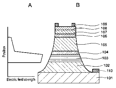
2o Fig. lA shows electric field strength in an APD of a first exemplary
embodiment of the present invention;
Fig. 1B shows a cross sectional view of the APD of the first exemplary
embodiment of the present invention;
Fig. 2 shows characteristics of materials that compose a superlattice
25 multiplication layer in the first exemplary embodiment of the present
invention;
Fig. 3 shows a band diagram of the superlattice multiplication layer in the
first exemplary embodiment of the present invention;
Fig. 4A shows electric field strength in the APD;
CA 02341110 2003-07-09
~a
Fig. 4B shows a cross sectional view of an AYD of a second exemplary
embodiment of the present invention;
Fig, SA shows an electric field strength in an A:I'D of the prior art; and
Fig. SB shows ~i cross sectiuna'I u~i~w of' the AIaD of the prior art,.
s
DESCRIPTLON OF THE PREFERRED EMBODIMENTS
FIRST EXEMPLARY EIVIBODItVIENT
With reference to accompanying cira.wings, a first ~;~emplary embodiment
of the present invewtion will be describeca.
Fig. 1B shows a cross sectional view of an AI'D of this exemplary
embodiment, and Fig. 1 A shows an electric field strength distribution when a
reverse bias voltage is applied to this APD.
In Fig. 1 B, the APD of present e:~etnplary ernl>odiment comprises:
t 5 (a) an n+-InP substrate 101;
(b) an n+-InP buffer layer 1 ~~q
(c) a distortion-compensated superlattice multiplication layer 103
comprising non-doped InXAI a_~As r InyCia,_yAs~,Pr.~;
CA 02341110 2001-03-16
6
(d) a p-type InP layer (sheet-doping layer) 104 having an impurity
concentration of 8 x 101' cm-3 and a thickness of 160 A;
(e) a p -type Ino,4~Gafl.53As light-absorbing layer 105 having an impurity
concentration of 2 x 1015 cm-3 and a thickness of 1 pm;
(f) a p+-Ino,4~Gao.53As layer :106 having an impurity concentration of 2 x
101'
cm-3 and a thickness of S00 A;
(g) a p+-InP window layer 107 having an impurity concentration of 1 x 101$
cm-3 and a thickness of 1000 ~~;
(h) a p+-Ino.4,GaoS3As contact layer 108 having an impurity concentration of
:LO 1 x 101$ cm 3 and a thickness of 1000 A;
(i) an AuZnNi electrode 109; and
(j) an AuGeNi electrode 110.
The APD in this invention is characterized by having the distortion-
compensated superlattice multiplication layer 103, where x, y, and z
respectively
:l5 satisfy the following conditions:
Osx<O.S2;
0.8<ysl; and
0 s z < 0.6.
a'.0 A method of manufacturing the APD of the present exemplary embodiment
is described below.
Individual layers composed of compound semiconductor material and
comprising the APD are fabricated by epitaxially growing each layer using a
gas-
source molecular beam epitaxy (MBE) method, and laminating them
5 consecutively on a pre-etched n+-InP substrate 101. The AuZnNi electrode 109
and the AuGeNi electrode 110 are fabricated by metal vacuum deposition and
photo-lithographic process.
Fig. 1A shows an electric, field strength distribution within an element
having
the structure described above, when a positive electric potential, that is the
reverse
30 bias voltage, is applied to its n-side. Under a condition where the reverse
bias
n
CA 02341110 2001-03-16
7
voltage is applied, light incident to the n+-InP substrate 101 is absorbed in
the
Ino.a~Gao.s3~ light-absorbing layer 105, and pairs of electrons and holes are
generated. The generated electrons move toward the superlattice multiplication
layer 103 responsive to the bias voltage applied between the AuZnNi electrode
109 and the AuGeNi electrode 110. Since the electric field strength is
concentrated in the layer 103, as shown in Fig. lA, the electrons injected
into the
layer 103 are accelerated, and thereby electronic multiplication occurs while
repeating impact ionization.
The layer 103 represents the distortion-compensated superlattice layer
composed of InXAII_XAs and InyGa,_y,AsZP~-Z having a band-gap energy of 1.45
eV
or greater. InyGal_yAsZP~-Z has a lattice constant, of which lattice-mismatch
with
respect to InP is opposite in direction to that of InXAII_XAs, and
discontinuity in a
valence band with InXAII-XAs is nearly zero.
Fig. 2 shows relations between lattice constant and band-gap energy of
various materials that compose the layer 103 in the APD of this exemplary
embodiment. Fig. 3 is a band diagram of the layer 103 in the APD of this
exemplary embodiment.
If the x is made smaller than 0.52 in InXAII_XAs, x = 0.44, for instance, the
a
lattice constant becomes 5.83 A, and the band gap becomes 1.75 eV, as shown in
:?0 Fig. 2. In the case of In~.Ga,_yAsZPI-Z, on the other hand, the lattice
constant
becomes 5.91 A, and the band gap becomes 1.1 eV, if y = 0.95 and z = 0.3. This
makes the layer 103 having a large discontinuity in the conduction band as
compared to any superlattice layer fabricated by the conventional method,
since a
difference in discontinuity of the conduction band becomes 0.65 eV while
~?5 maintaining zero discontinuity in the valence band, as shown in Fig. 3.
Although the superlattic:e layer of the prior art has an ionization rate of
electrons large enough against an ionization rate of holes, the distortion-
compensated superlattice multiplication layer introduced by the present
invention
has an ionization rate of electrons far in excess of the conventional one. In
ai0 addition, since a band gap of a well layer and a band gap of a barrier
layer become
CA 02341110 2001-03-16
g
larger than thase of the conventional superlattice, an effective band gap as
the
superlattice is increased, and therefore a dark current due to the tunnel
current
decreases.
In the APD of the present invention, the electric field strength applied to
the
superlattice multiplication layer is increased as compared with the
conventional
one, because reverse bias voltage can be increased as the dark current
decreases.
It is obvious when the electric field strength distribution of the APD of this
invention shown in Fig. 1A is compared with Fig. SA representing an electric
field
strength distribution of the API) of the prior art.
According to the APD of the present invention, discontinuity in a valence
band is made nearly zero by introducing InGaAsP layer as a well layer, while
strain is introduced to the superlattice multiplication layer to increase DEc.
Accordingly, a large multiplication factor can be obtained while the dark
current is kept suppressed. On the other hand, it is significance to obtain
the
large multiplication factor while keeping the dark current suppressed, in a
sense
that it realizes a reduction of a superlattice period of the superlattice
multiplication
layer, because it is equivalent to a large ionization rate of electrons. As a
result, a
layer thickness of the superlattice layer can be decreased to shorten a moving
time
of electrons, and thereby the high frequency response can be obtained.
:ZO With the structure as described above, pure electronic multiplication is
realized without increasing the multiplication noise in the layer 103, and
hence
performance of the superlattice APD is enhanced.
In this exemplary embodiment, although InyGa1_yAsZPI-Z, is used as a material
of the well layer in the superlattice multiplication layer, this material may
be
:~5 substituted by InGaAlAs to obtain similar characteristics by controlling
the
composition of In, Ga Al and As.
SECOND EXEMPLARY EMBODIMENT
Referring now to the accompanying drawings, a second exemplary
30 embodiment of the present invention will be described.
CA 02341110 2001-03-16
9
An APD of this exemplary embodiment is characterized by having a
reflective rnulti-layer structure in order to improve a utilization efficiency
of
incident light in the first exemplary embodiment. Fig. 4B shows a cross
sectional
view of the APD of this exemplary embodiment, and Fig. 4A shows an electric
field strength distribution when a reverse bias voltage is applied to this
APD.
In Fig. 4, the APD of this exemplary embodiment comprises:
(a) an n+-:fnP substrate 401;
(b) an n+-InP buffer layer 402;
(c) a distartion-compensated superlattice multiplication layer 403 comprising
nondoped InXAlI-XAs / InyGal-,~,AszPl-Z;
(d) a p-type InP layer (sheet-doping layer) 404 having an impurity
concentration of 8 x 10" cm-3 and a thickness of 160 A;
(e) a p -type Ino.4~Gao.s3As light-absorbing layer 405 having an impurity
concentration of 3 x 10'5 cm-=' and a thickness of 0.4 Vim;
(f) a p+-type Ino.s~Alo.as~ / Ino.sGao.2~o.6Po.a mufti-layered light-
reflecting
layer 406 having an impurity concentration of 1 x 101 cm-3v
(g) an AuZnNi electrode 407; and
(h) an AuGeNi electrode 408.
In the foregoing structure, values x, y, and z of the distortion-compensated
:?0 superlattice multiplication layer 403 respectively satisfy the same
conditions as
those of the first exemplary embodiment.
A method of fabricating the element of this exemplary embodiment is same
as what has been described in the first exemplary embodiment.
Of all light incident to the n+-InP substrate 401, a part not absorbed in the
~?5 light-absorbing layer 405 is reflected by the mufti-layered light-
reflecting layer
406, and then absorbed in the light-absorbing layer 405 as it again passes
therethrough. The mufti-layered light-reflecting layer 406 of this embodiment,
because it uses a mufti-layered structure, can reflect the light efficiently,
as it gains
a reflectivity of 99% or higher, whereas a reflection surface of a metal
electrode
BO used in the prior art can not obtain sufficient reflection of light since
it has a
CA 02341110 2001-03-16
reflectivity of only about SO %. As a result, the present element produces a
standing wave between a light entrance plane and the mufti-layered light-
reflecting
layer 406, so as to increase an absorption efficiency in the light-absorbing
layer
405, and hence a quantum efficiency at the same time. For this reason, the
5 quantum efficiency of the light-absorbing layer 405 does not decrease, even
though its layer thickness is one quarter or less of 2 p.m, which is a
reciprocal
number of the absorption coefficient of 1.55 p,m wave length light. On the
other
hand, a response of the APD improves, since the layer thickness of the light
absorbing layer 405 is reduced, which shortens a traveling distance of
carriers
10 generated by injection of the light.
Although what has been described above is an example, in which the light-
absorbing layer 405 has a layer thickness of 0.5 p,m, it has been verified
that a
light-reflecting film of 60 ~o or greater in reflectivity can be obtained with
a light-
absorbing layer 405 having a layer thickness of 0.8 pm or less.
In other words, the layer thickness of the light-absorbing layer 405 can be
reduced to 80 % or less in this exemplary embodiment, though the conventional
structure had required the light-absorbing layer to have a layer thickness of
one
half of a reciprocal number (2' hum) of an absorption coefficient for 1.55 p,m
wave
length light.
:ZO The APD of this exemplary embodiment is basically identical in other
structural and operational features to those of the first exemplary
embodiment,
except that it is provided with the reflective mufti-layered structure. In
addition,
the above function can be provided independently with that of the first
exemplary
embodiment.
:~5 A method of fabricating a mufti-layered light-reflecting layer of this
exemplary embodiment will be described hereinafter.
A method of fabricating the individual layers composed of compound
semiconductor materials comprising the APD has been described previously. A
mufti-layered light-reflecting layer can be formed consecutively by the gas-
source
a30 MBE after the above APD element is formed. Alternatively, a
photolithographic
CA 02341110 2001-03-16
11
method may be used to form a window, after forming an AuZnNi electrode 109,
and the mufti-layered light-reflecting layer may be formed on it. A material
of
the mufti-layered light-reflecaing layer needs not be limited to the compound
semiconductor, and it can be formed by laminating dielectric material or the
like
by any other known thin-film forming methods such as the sputtering, CVD and
the like, when forming it after formation of the AuZnNi electrode 109.
As a result, this exemplary embodiment is not only capable of increasing the
response of APD without decreasing the quantum efficiency in the light-
absorbing
layer 405, but is also able to maintain the effectiveness of the distortion-
compensated superlattice multiplication layer described in the first exemplary
embodiment. Since both of these features can coexist together, as noted above,
the APD having even faster response and higher sensitivity is obtained.
In the avalanche photodiode employing the superlattice structure as an
avalanche multiplication layer, an introduction of the distortion-compensated
superlattice structure for the superlattice layer makes it possible to reduce
a layer
thickness of the superlattice multiplication layer without decreasing the
multiplication factor and increasing the dark current, as stated above. As a
result,
an operating voltage can be reduced, in addition to increasing the response.
In
addition, even i:urther improvement of the high-speed response and high
sensitivity
is obtained by concurrently adopting the reflective mufti-layer film
structure.