Note: Descriptions are shown in the official language in which they were submitted.
CA 02341815 2004-11-22
Two-Dimensional Photonic Crystal, and
Multiplexer/Demultiplexer Using the Same
TECHNICAL FIELD
This invention relates to a photonic crystal for use
as a ultrasmall optical circuit device, and more
particularly, to a two-dimensional photonic crystal having
a two-dimensional periodic distribution of refractive
index. It further relates to a waveguide having a light or
electromagnetic radiation outlet/inlet port created by
introducing a line defect and a point defect in such
photonic crystal, and a wavelength demultiplexer.
BACKGROUND ART
With the recent advance of wavelength multiplexing
communication systems, wavelength demultiplexers,
multiplexers and filters become more important.
The optical branching/inserting device for wavelength
multiplexing communication systems, also known as optical
add/drop multiplexing device, has a function of taking a
signal of a certain channel out of multiplexed signals or
add the same to an empty channel. General constructions
include array waveguide diffraction grating and fiber
grating types. The array waveguide diffraction grating is
a kind of diffraction grating having an array of a
plurality of optical waveguides of different length in
which the difference in length between waveguides creates a
wavelength-dependent slope of wavefront so that upon input
of wavelength-multiplexed light, the light is demultiplexed
in terms of wavelength into different waveguides to produce
outputs (see Journal of IEICE, pp. 746-749, 1999, for
example). In the fiber grating type, only signals of a
specific wavelength are taken out of the drop port or
introduced from the add port by Bragg reflection at the
1
CA 02341815 2001-03-23
fiber grating.
In the prior art wavelength
multiplexers/demultiplexers of the array waveguide
diffraction grating type, however, the radius of curvature
must be kept significantly large in order to reduce a bend
loss, resulting in a very large device size.
Many proposals were then made based on the concept of
forming an ultrasmall optical multiplexer/demultiplexer
using photonic crystal. These proposals are described in,
for example, Applied Physics Letters, vol. 75, pp. 3739-
3741, 1999 (Reference 1) and Physical Review Letters, vol.
80, pp. 960-963, 1998 (Reference 2).
The photonic crystal is a crystal having a periodic
distribution of refractive index therein, which enables to
establish novel optical characteristics using an artificial
periodic structure.
One of the important features of the photonic crystal
is the presence of a photonic bandgap. In photonic crystal
having a three-dimensional periodicity (referred to as a 3D
photonic crystal, hereinafter), a full bandgap that
prohibits propagation of light in all directions can be
formed. This enables local confinement of light, control
of spontaneous emission light, and formation of a waveguide
by the introduction of a line defect, indicating a
possibility to realize an ultrasmall optical circuit.
Reference 1 suggests that an ultrasmall light
demultiplexer can be formed by branching a waveguide formed
by introducing a line defect into a 3D photonic crystal,
but does not illustrate any specific structure.
Active studies have been made on a photonic crystal
having a two-dimensional periodic structure (referred to as
a 2D photonic crystal, hereinafter), because its
fabrication is relatively easy. Reference 2 describes the
analytic results of a demultiplexer using a branched
waveguide.
A refractive index periodicity structure of 2D
-2-
CA 02341815 2001-03-23
photonic crystal is formed by arranging cylindrical holes
in a high refractive index material in a square or
triangular lattice pattern. Alternatively, it is formed by
arranging cylinders of a high refractive index material in
a low refractive index material in a square lattice
pattern. Photonic bandgaps are formed from these
periodicity structures whereby the propagation of in-plane
light is controlled. By introducing a line defect into
this periodic structure, a waveguide can be created. See,
for example, Physical Review Letters, vol. 77, pp. 3787-
3790, 1996, and Reference 2.
Reference 2 relates to the array of cylinders of a
high refractive index material in a square lattice pattern.
It is noted that although the propagation of light in the
in-plane direction can be controlled by a bandgap as
previously described, the propagation of light in upward
and downward directions cannot be controlled by the
periodic structure. Analysis is thus made on a straight
waveguide and a 90° bend branch configuration and branch
configuration on the assumption that the height is
infinite.
However, since it is impossible for an actual device
to have an infinite height, light must be confined within a
finite height.
On the other hand, where cylindrical holes are formed
in a high refractive index material, a waveguide can be
created by forming the high refractive index material as a
slab, and providing low refractive index layers above and
below the slab so as to confine light by total reflection.
However, no research has been made on multiplexers
and demultiplexers of such a structure. Also, no research
has been made on the 90° bend branch configuration and
branch configuration of guiding light propagating in the
in-plane direction to the orthogonal direction or guiding
light from the orthogonal direction to the in-plane
direction.
-3-
CA 02341815 2001-03-23
Optical multiplexers and demultiplexers using a
super-prism based on self-organized 3D crystal have also
been studied. See, for example, Applied Physics Letters,
vol. 74, pp. 1212-1214, 1999 and 0 plus E, December 1999,
pp. 1560-1565. They are not combined with waveguides, and
only the function of an independent device is investigated.
If a photonic crystal waveguide is able to deliver a
light output with wavelength selectivity in a certain
wavelength region or receive a light input with wavelength
selectivity, it becomes possible to realize an optical
circuit having a light demultiplexing/multiplexing function
of much smaller size than conventional devices. Also, if
light or electromagnetic radiation in a 2D photonic crystal
waveguide can be guided to the orthogonal direction, a
steric light or electromagnetic radiation circuit can be
obtained.
SUMMARY OF THE INVENTION
An object of the invention is to provide a
construction capable of guiding or receiving light or
electromagnetic radiation propagating through a 2D photonic
crystal waveguide in a direction orthogonal to the plane
thereof, the construction being effective for forming a
light or electromagnetic radiation waveguide or a light or
electromagnetic radiation multiplexer/demultiplexer.
The above and other objects are attained by the
invention which is defined below.
(1) A two-dimensional photonic crystal waveguide
comprising
a two-dimensional photonic crystal structure based on
a slab formed of a material having a higher refractive
index than air, in which a material having a lower
refractive index than the slab material is periodically
arrayed to provide a refractive index distribution,
a photonic crystal waveguide created by forming a
line defect in the periodic array of photonic crystal, the
line defect functioning as a waveguide, and
-4-
CA 02341815 2001-03-23
at least one point defect disposed adjacent the
photonic crystal waveguide to act as a disorder in the
periodic array of photonic crystal,
wherein the point defect functions as a light or
electromagnetic radiation outlet/inlet port for trapping
light or electromagnetic radiation of a selected wavelength
among light or electromagnetic radiation propagating
through the waveguide and radiating it, or trapping light
or electromagnetic radiation of a selected wavelength from
without the waveguide and introducing it into the
waveguide.
(2) The two-dimensional photonic crystal waveguide of
(1) wherein the light or electromagnetic radiation
outlet/inlet port is to radiate or introduce the light or
electromagnetic radiation propagating in a direction
orthogonal to the slab surface.
(3) The two-dimensional photonic crystal waveguide of
(1) or (2) wherein the wavelength of light or
electromagnetic radiation radiated or introduced by the
point defect differs depending on the shape of the point
defect .
(4) The two-dimensional photonic crystal waveguide of
any one of (1) to (3) wherein the array of the lower
refractive index material is formed by filling cylindrical
holes in the slab with the lower refractive index material.
(5) The two-dimensional photonic crystal waveguide of
any one of (1) to (4) wherein the array of the lower
refractive index material is a triangular lattice array.
(6) The two-dimensional photonic crystal waveguide of
any one of (1) to (5) wherein the point defect is
configured so as to be asymmetric on opposite sides with
respect to the slab surface.
(7) The two-dimensional photonic crystal waveguide of
any one of (1) to (6) wherein the slab material has a
refractive index of at least 2Ø
(8) The two-dimensional photonic crystal waveguide of
-5-
CA 02341815 2001-03-23
(7) wherein the slab material is an inorganic material
containing at least one element selected from the group
consisting of In, Ga, A1, Sb, As, Ge, Si, P, N, and O or an
organic material.
(9) The two-dimensional photonic crystal waveguide of
any one of (1) to (8) wherein the lower refractive index
material is air.
(10) A photonic crystal wavelength demultiplexer
comprising the two-dimensional photonic crystal waveguide
of any one of (1) to (9).
(11) The photonic crystal wavelength demultiplexer of
(10) wherein there are included a plurality of point
defects and wavelength of light or electromagnetic
radiation radiated or trapped by each point defect differs.
(12) The photonic crystal wavelength demultiplexer of
(10) or (11), further comprising an optical fiber disposed
in proximity to the point defect.
(13) The photonic crystal wavelength demultiplexer of
(10) or (11), further comprising a semiconductor device
having a photoelectric conversion function disposed in
proximity to the point defect.
In the 2D photonic crystal waveguide of the invention
comprising a 2D photonic crystal structure based on a slab
formed of a material having a higher refractive index than
air, in which a material having a lower refractive index
than the slab material is periodically arrayed to provide a
refractive index distribution, a photonic crystal waveguide
is created by forming a line defect, which functions as a
waveguide, in the periodic array of photonic crystal, and
at least one point defect is disposed adjacent the photonic
crystal waveguide to act as a disorder in the periodic
array of photonic crystal. The point defect functions as a
light or electromagnetic radiation outlet/inlet port for
trapping light or electromagnetic radiation of a selected
wavelength among light or electromagnetic radiation
propagating through the waveguide and radiating it, or
-6-
CA 02341815 2004-11-22
trapping light or electromagnetic radiation of a selected
wavelength from the exterior and introducing it into the
waveguide.
The waveguide and the point defect according to the
invention can transport, receive .and deliver not only
light, but also electromagnetic radiation having a
character approximate to light.
Where a point defect is formed in proximity to the
waveguide formed by the line defect, introduction and
removal of light or electromagnetic radiation into and out
of the point defect becomes possible so that a light or
electromagnetic radiation inlet/outlet port is available.
The point defect becomes a disordered site in the 2D
photonic crystal structure based on a slab formed of a
material having a higher refractive index than air, in
which a material having a lower refractive index than the
slab material is periodically arrayed to.provide a
refractive ir~dex dis;~ribution.
Accordingly, in one aspect, the invention provides a
two-dimensional photonic crystal comprising a two-
dimensional photonic crystal structure based on a slab
formed of a slab material having a higher refractive index
than air, in which an array material having a lower
refractive index than the slab material is periodically
arrayed into the slab to provide a refractive index
distribution, a photonic crystal waveguide created by
forming a line defect in the periodic array of the photonic
crystal, the line defect functioning as a waveguide, and at
least one point defect disposed adjacent the line defect to
act as a disorder in the periodic array of the photonic
crystal, wherein the at least one point defect functions as
a light or electromagnetic radiation outlet/inlet port for
trapping light or electromagnetic radiation of a selected
wavelength among light or electromagnetic radiation
CA 02341815 2004-11-22
propagating through the waveguide and radiating the trapped
light or electromagnetic radiation along a direction that
intersects the slab, or trapping light or electromagnetic
radiation of a selected wavelength received along the
direction that intersects the slab from outside the
waveguide and introducing the trapped light or
electromagnetic radiation into the waveguide.
In another aspect, the invention provides a photonic
crystal multiplexer/demultiplexer comprising the two-
dimensional photonic crystal waveguide as previously
described herein.
BRIEF DESCRIPTION OF THE DRAWINGS
FIG. 1 is a schematic perspective view showing a 2D
photonic crystal slab waveguide having one point defect
according to one embodiment of the invention.
FIG. 2 is a schematic perspective view showing a 2D
photonic crystal slab waveguide having two point defects
according to another embodiment of the invention.
FIG. 3 is a schematic plan view showing the
triangular lattice pattern of the 2D photonic crystal slab
waveguide of FIG. 1.
FIG. 4 is a schematic plan view showing the square
lattice pattern of the 2D photonic crystal slab waveguide
FIG. 5 is a fragmentary cross-sectional view of
another form of point defect.
FIG. 6 is a fragmentary cross-sectional view of a
further form of point defect .
FIG. 7 is a schematic perspective view of a surface
7a
CA 02341815 2001-03-23
output type wavelength demultiplexer according to the
invention.
FIG. 8 is a schematic perspective view of another
surface output type wavelength demultiplexer according to
the invention.
FIGS. 9 to 14 are cross-sectional views showing
successive steps of a process of fabricating a 2D photonic
crystal InGaAsP slab waveguide.
FIGS. 15 to 20 are cross-sectional views showing
successive steps of another process of fabricating a 2D
photonic crystal InGaAsP slab waveguide.
FIG. 21 is a perspective view showing dimensions
associated with a 2D photonic crystal.
FIG. 22 is a graph showing the frequency and
intensity of light or electromagnetic radiation radiated in
the orthogonal direction from the point defect disposed
adjacent to the 2D photonic crystal slab waveguide of FIG.
1.
FIG. 23 is a graph showing the frequency and
intensity of light or electromagnetic radiation radiated in
the orthogonal direction from the two point defects
disposed adjacent to the 2D photonic crystal slab waveguide
of FIG. 2.
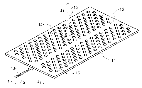
Referring to FIG. 1, there is illustrated a
waveguide/wavelength demultiplexer according to a first
embodiment of the invention in which a point defect is
disposed adjacent to a two-dimensional photonic crystal
slab waveguide for delivering light or electromagnetic
radiation of a selected wavelength in an orthogonal
direction. Throughout the specification, directions
parallel and orthogonal to a major surface of the two-
dimensional photonic crystal slab are referred to as in-
plane and orthogonal directions, respectively.
First, the photonic crystal and the waveguide are
described. The photonic crystal used herein is a 2D
photonic crystal having a bandgap in an in-plane direction
_g_
CA 02341815 2001-03-23
due to a 2D periodic distribution of refractive index, and
is structured such that cylindrical holes 16 are arrayed in
a slab material 11 in a triangular lattice pattern as shown
in FIG. 1.
Incident light or electromagnetic radiation 13 (~1,
~2, ... Vii, ...) within the crystal, is prevented by the
bandgap from propagating in the in-plane direction, and
confined in the orthogonal direction due to total
reflection by upper and lower low refractive index
materials.
As shown in FIG. 1, a line defect 12 is incorporated
in the photonic crystal by linearly removing some of the
cylindrical holes 16 arrayed in the triangular lattice
pattern. In the line defect 12, a guided mode exists to
form a waveguide.
The material of which the photonic crystal slab
structure is formed is desirably a material having a high
refractive index because of the need to confine light or
electromagnetic radiation in upward and downward
directions. Although an InGaAsP slab is used in the
illustrated embodiment, there may be used GaAs, a material
containing one or more elements selected from among In, Ga,
A1, Sb, As, Ge, Si, P, N, and O, an inorganic material such
as Si, especially an inorganic semiconductor material, or
an organic material.
The material used as the slab should desirably have a
higher refractive index as mentioned above, specifically
higher than air, preferably at least 2.0, and more
preferably at least 3Ø
In the illustrated embodiment, the cylindrical holes
16 are arrayed in a pattern of triangular lattices 16a as
shown in FIG. 3, although it is possible to use a photonic
crystal in which the cylindrical holes 16 are arrayed in a
pattern of square lattices 16b so that a photonic bandgap
is present and a defect 12 is linearly incorporated as
shown in FIG. 4. It is noted that FIGS. 3 and 4 each are a
-9-
CA 02341815 2001-03-23
plan view of a portion of the photonic crystal-constructing
slab.
Next, the light or electromagnetic radiation
outlet/inlet port is described. As previously described,
light or electromagnetic radiation can propagate through a
defect waveguide in the 2D photonic crystal. In a linear
waveguide, the wavelength range in which light or
electromagnetic radiation can be transported at a low loss
is relatively wide. Then light or electromagnetic
radiation in a wavelength region including the wavelengths
of several channels can be transported through the
waveguide. By contrast, once a point defect 14 is disposed
in proximity to the waveguide as shown in FIG. 1, light or
electromagnetic radiation of a selected wavelength is
trapped within the defect. While resonating within the
defect, the light or electromagnetic radiation 15 is
radiated in upward and downward directions having a low Q
factor due to the slab shape.
By designing the point defect so as to trap only the
wavelength of a particular channel in the wavelength
region, the point defect functions not only as the light or
electromagnetic radiation outlet/inlet port, but also as a
demultiplexer, multiplexer or filter for taking out light
or electromagnetic radiation of the selected wavelength
(~i). With this configuration, the in-plane guided light
or electromagnetic radiation can be guided in the
orthogonal direction, enabling to form a branching or
redirecting path within a minute region. Inversely, light
or electromagnetic radiation of a selected wavelength
incoming in the orthogonal direction can be guided to the
in-plane waveguide.
By appropriately setting the spacing between the
waveguide and the point defect, it becomes possible to
control the proportion of light or electromagnetic
radiation of a selected wavelength to be trapped and
radiated. It is then possible to form with ease a light or
-10-
CA 02341815 2004-11-22
electromagnetic radiation circuit for taking out or
branching a predetermined proportion of light or
electromagnetic radiation.
In the embodiment of FIG. 1, light or electromagnetic
radiation is radiated in upward and downward directions
because the defect lacks vertical asymmetry. Vertical
asymmetry can be incorporated in the defect so that light
or electromagnetic radiation is radiated in either one of
upward and downward directions. The method of
incorporating asymmetry is, for example, by tailoring the
shape of the point defect 14 from cylinder to cone as shown
in FIG. 5, or by changing the diameter of the point defect
14 between upper and lower levels of the slab 11 as shown
in FIG: 6. It is noted that FIGS. 5 and 6 each are a
cross-sectional view of a point defect-surrounding portion.
Referring to FIG. 2, there is illustrated a second
embodiment of the invention wherein two point defects 21
and 22 are disposed adjacent to the linear waveguide.
Since the wavelength of light or electromagnetic radiation
24, 25 to be trapped or radiated is controlled by the size
of each defect, two wavelengths (~,i, ~.j) in the region of
incident light or electromagnetic radiation 23 (A1, 1~2, , , , ,
~;i, 7~.j, ...) can be delivered through the respective point
defects. The light or electromagnetic radiation other than
the trapped and radiated ones is guided through the linear
waveguide. Although a two-channel wavelength demultiplexer
is illustrated in this embodiment, a multi-channel
wavelength demultiplexer can be formed by increasing the
number of defects.
FIG. 7 illustrates the concept of a
multiplexer/demultiplexer according to a third embodiment
of the present invention. Light or electromagnetic
radiation 31 of a certain wavelength region propagates
through the photonic crystal waveguide, is trapped by point
defects 32 to 34 and delivered in the orthogonal direction.
The light or electromagnetic radiation is introduced
11
CA 02341815 2001-03-23
into optical fibers 35 to 37 disposed above the point
defects and used as signals. The optical fibers are
preferably located above the point defects with a
sufficient spacing not to cause the photonic crystal
structure to be disordered.
Alternatively, the photonic crystal structure may be
integrated with semiconductor devices having a
photoelectric conversion function, for example, photodiode
arrays 45 to 47 as shown in FIG. 8. With this
construction, light or electromagnetic radiation delivered
from the point defects 42 to 44 in the orthogonal direction
can be directly converted into electrical signals within
very small areas.
Now it is described how to fabricate a photonic
crystal waveguide/wavelength demultiplexer according to one
embodiment of the invention.
First of all, as shown in FIG. 9, on an InP substrate
51, for example, an InP layer 52 serving as a buffer layer
and a layer of a high refractive index material, typically
an InGaAsP layer 53 are formed by crystal growth. Crystal
growth is preferably carried out by the MOCVD method and at
590 to 650°C.
Next, to form a triangular lattice pattern of
circular holes and point defects, a photoresist 54 for
electron beam patterning is coated as shown in FIG. 10,
which is exposed and developed into a resist pattern as
shown in FIG. 11. Image exposure with electron beams is
employed herein since the lattice constant of the photonic
crystal is as small as about 0.5 ~m at most even on the
assumption that the light or electromagnetic radiation to
be transported has a wavelength in the infrared region.
Next, as shown in FIG. 12, cylindrical holes and
defects are formed in the InGaAsP slab by reactive ion
etching (RIE) using the resist as a mask. The RIE uses a
gas mixture of HZ and CH4, for example.
The resist is then removed as shown in FIG. 13. In
-12-
CA 02341815 2001-03-23
order to provide air layers having a low refractive index
above and below the slab, the InGaAsP slab is processed
into a membrane as shown in FIG. 14. This is done by wet
etching so as to effect selective etching of the InP layer.
Although InGaAsP is used as the high refractive index
material in the above example, silicon (Si) is also useful
because it has a high refractive index and can be processed
by micro-machining. The fabrication method using Si as the
slab material is described below.
First, there is furnished a silicon-on-insulator
(SOI) substrate as shown in FIG. 15. The SOI substrate
includes a Si substrate 61 serving as a base and a single
crystal Si layer 63 stacked thereon with a SiOz layer 62
interposed therebetween. Instead of the SOI substrate, a
structure having a Si02 layer and a Si layer grown on a Si
substrate is also employable. Next, a photoresist 64 for
electron beam patterning is coated as shown in FIG. 16,
which is exposed and developed into a resist pattern as
shown in FIG. 17.
Next, as shown in FIG. 18, cylindrical holes and
defects are formed in the Si layer 63 by reactive ion
etching (RIE) using the resist 64 as a mask. The RIE uses
SF6 gas. Then the resist is removed as shown in FIG. 19.
The oxide film layer below the photonic crystal is etched
with an aqueous HF solution, leaving a membrane as shown in
FIG. 20.
EXAMPLE
Illustrative examples of the invention are described
below together with their characteristics.
First described is a photonic crystal. The photonic
crystal slab was formed of InGaAsP. For example, as shown
in FIG. 21, the photonic crystal has a lattice constant
"a," the holes have a radius r of 0.29a, and the slab has a
thickness t of 0.6a.
On the slab provided with a line defect and a point
defect, analysis was conducted by the finite-difference
-13-
CA 02341815 2001-03-23
time-domain (FDTD) method, with the results shown below.
It is understood that the FDTD method is a method of
directly solving the time-dependent rotational equation
among the Maxwell's equations, which is briefly explained
below.
In an isotropic medium, the Maxwell's equations is
described as follows.
oXE=-~aa
oXH=+EaE
at
Herein, ~, is a permeability, E is a dielectric
constant.
From these equations, the following six difference
equations are obtained.
-14-
CA 02341815 2001-03-23
-i N
W
.-~
I
N
+ .~IN
wN ~ ~ N
I a I
W
-~
~
N
a~ .-~
I
N
-I-
N ~.
yS
.-.
I
N
~IN +
U
I N I
d ~y d
r.
I
N
x
'_"IN
w
~
_i
~?, ~N
I I I 1
.~IN ~IN
." ~
d ,-~ I d .'
N
~
I
N
'-' ~~ '-
I I
N N
.-~~N+ ~'IN
r,IN
.-~ + ~ ~
~ I
N N
-f- ''~ .~ ~ N
~ ~ +
_ _
N .~
~ N
I
.~+NI .-+t~l
Z ~
k
~ II II
-15-
CA 02341815 2001-03-23
m ~-
~~m
i
~
I
~''INi
+
I
.
+ w
...
+N
H t
?.
+
W ~ .~IN
I
'~ .-r
I I
N rl
+
.~
N
W~. +
n
~IN I
i
+ .,
I
c n
,~ '~
W I
N
+
;
i
_ Z
N
+
.--~ x
~
N
+_ ~IN,
+
a .,
,~
W
i i ,-,
I
N
+
~i
.-IN
+ f
N
i i
+
,+ - a -
I
N
+
.~ w
I
CV
-, + +
~
N
+
..-.
I n
N
-i~N + SIN ,_I
N
+ ~ + +
_ IN
SIN Z
N ~Y,
N
W II
-16-
CA 02341815 2001-03-23
Ln
.-. ,-~
I I
N N
y
-, ,-i
I I
N N
y
~IN
f
N .~
~
N
as
.--~ .-
I I
N N
az
.~IN .-,IN
I
I
H
.-.
I .-.
N I
+ N
N
f
.~ ,
I
N
I
.~IN
.-.
I
N
I
U
... ~-IN
I
N
f
~i f_
N
I
,~IN
,~IN
+
~IN
+ .-~
I
N
,..IN
~
~
nl
G +
N I Z
N 1
I
L
..-I
I
N
.~IN +
d .f-
\
..~
.~IN .-.IN
r.. ,-. + +
I I
N N
f W?, .f ~iN
W~ I W J
I
CA 02341815 2001-03-23
Using the above six equations, the way of propagation
of light or electromagnetic radiation through the photonic
crystal slab can be analyzed. By observing an electric
field above the defect and conducting Fourier
transformation, its frequency spectrum is obtainable.
First described is a linear waveguide with a
cylindrical hole corresponding to one period removed. As
long as the normalized frequency f is in the range of 0.27
to 0.28 (c/a), light or electromagnetic radiation can
propagate through a waveguide without a loss. The lattice
constant is determined so that the wavelength of light or
electromagnetic radiation to be propagated may meet this
condition. In this example, the wavelength of light or
electromagnetic radiation to be propagated is set to be
1.55 Vim, f = 0.275 (c/a) corresponding to the center of the
range of 0.27 to 0.28 (c/a) is 1.55 Vim, then "a" is
computed to be 0.42625 ~m from 0.275x1.55 Vim.
FIG. 22 shows the frequency and intensity of light or
electromagnetic radiation radiated in the orthogonal
direction from the point defect disposed adjacent to the
waveguide. It is understood that the point defect is
provided by changing the radius of one cylindrical hole to
0.56a. It is seen from the diagram that light or
electromagnetic radiation at the normalized frequency f =
0.273 (c/a) is radiated in upward and downward directions.
The Q value is approximately 500.
FIG. 23 shows the frequency and intensity of light or
electromagnetic radiation radiated from each point defect
in the embodiment of FIG. 2 wherein point defects of
different size are disposed adjacent to the waveguide. In
this example, the point defects are cylindrical holes
having a radius of 0.56a and 0.58a. It is seen that light
or electromagnetic radiation at the frequency f = 0.2729
(c/a) and f = 0.2769 (c/a) is radiated. The Q value of
the defects is approximately 500 in either case.
It is confirmed from these results that a waveguide
-18-
CA 02341815 2004-11-22
created.by introducing a line defect and a point defect in
the 2D photonic crystal has a function of transmitting
light or electromagnetic radiation into and out of the
point defect and a function as a wavelength
demultiplexer/multiplexer of the plane output type.
A wavelength demultiplexer fabricated by providing a
point defect in proximity to a 2D photonic crystal
waveguide according to the invention is able to input and
output light or electromagnetic radiation in the orthogonal
direction despite the 2D photonic crystal structure. Since
light or electromagnetic radiation of a selected wavelength
can be input or output from the point defect in a
demultiplexed manner, there can be realized an ultrasmall
wavelength demultiplexer. This also enables relatively
easy realization of a steric ultrasmall light or
electromagnetic circuit.
Although some preferred embodiments have been
described, many modifications and variations may be made
thereto in light of the above teachings. It is therefore
to be understood that the invention may be practiced
otherwise than as specifically described without departing
from the scope of the appended claims.
-19-