Note: Descriptions are shown in the official language in which they were submitted.
CA 02342413 2001-04-23
62957-375D
-1-
A METHOD OF ISOLATING AN ELECTRICAL FAULT
This is a divisional application of Canadian Patent
application serial No. 2,250,751 entitled Combined Laser/FLIR
Optics system filed April 1St 1997.
BACKGROUND
The present invention relates to a combined forward-
looking infrared/laser sensor. More particularly, the present
invention relates to a targeting and imaging system that
combines a mid-wave forward-looking infrared (FLIR) subsystem
and a laser subsystem, including a laser range receiver (LRR)
and a laser spot tracker (LST).
FLIR systems employ an array or infrared (IR)
detectors for generating an image based on the IR emissions
from a particular area of interest (AOI). In military
applications, for example, the AOI may contain targets such as
tanks, trucks, and/or other military vehicles or military
hardware. These targets emit heat; therefore, they are
typically warmer than their surrounding environment.
Consequently, they can be distinguished in an IR image
generated by a FLIR system.
The use of lasers in conjunction with FLIR systems is
generally well known in the art. For example, lasers can be
used to designate specific targets which are visible in a FLIR
image. In one prior FLIR/laser system, laser energy is swept
across a target that is visible in the FLIR image and used for
the purpose of generating a 3-D image of the target. The 3-D
image can, in turn, be used for target recognition and/or
target classification (U. S. Patent No. 5,345,304). In another
CA 02342413 2001-04-23
62957-375D
-la-
prior FLIR/laser system, a laser is used for determining the
range of a target from the FLIR/laser system's host platform
(U. S. Patent No. 4,771,437). In yet another prior FLIR/laser
system, a laser is used to determine the relative position and
velocity of targets (U. S. Patent No. 4,5'74,191). In addition,
lasers have been used for the purpose of directing laser guided
munitions to a desired target visible in a FLIR image.
In each of the aforementioned prior FLIR/laser
systems, the ability of the FLIR/laser system to accurately
_ CA 02342413 2001-04-23
-2-
recognize, detect, locate and/or track targets is dependent
upon the ability of the system to maintain an accurate
alignment between the FLIR and laser. Any fixed
misalignment between the FLIR line-of-sight (LOS) and the
laser LOS will result in laser overspill. As illustrated in
FIG. 1, laser overspill is defined as the unintended amount
of laser energy 110 that misses the target 105 and reflects
off the background. Laser overspill is likely to result in
range measurement error, as illustrated by Re=.=. in FIG. 2.
False range information, in turn, will result in less
accurate target recognition, detection, location, and
velocity information, as well as less accurate weapon
guidance data.
Boresighting is a common term of art which refers to
the process of aligning the LOS of a given system. Prior
designs, such as the Low Altitude Night Terrain-following
Infrared Navigation (LANTIRN) system, employ boresighting
processes to minimize fixed alignment errors between the
FLIR LOS and the laser LOS. Boresighting processes
typically involve optical and/or mechanical realignment of,
for example, the FLIR LOS and the laser LOS. Moreover,
boresighting processes may be manual or they may be
automatic. As stated, boresighting processes are generally
well known in the art.
Unfortunately, the alignment error between, for
example, a FLIR LOS and a laser LOS is not necessarily a
fixed error. In military applications, FLIR/laser based
systems are typically installed on moving platforms, such as
tactical aircraft (e. g., an F-15 or an F-16). These
platforms subject the FLIR/laser based system to large
mechanical forces and vibrations. These forces and
vibrations directly act upon the optical components which
govern the FLIR LOS and the laser LOS. Moreover, FLIR LOS
and laser LOS displacements about the pitch axis appear to
have the most detrimental affect on system performance
CA 02342413 2001-04-23
-3-
(i.e., the ability to accurately recognize, detect, locate
and/or track targets).
As illustrated in FIG. 3, prior designs such as LANTIRN
employ a separate FLIR optics pitch bearing 205 and laser
optics pitch bearing 210, as well as a separate FLIR
aperture 215 and laser aperture 220. Consequently, the
aforementioned mechanical forces and vibrations acting upon
the FLIR/laser based system will cause the FLIR LOS and the
laser LOS to nutate about the pitch axis independent of each
other, resulting in LOS fitter and a dynamic (i.e.,
continuously changing) FLIR LOS-to-laser LOS alignment error
in addition to any exiting fixed alignment error. Although
the boresighting processes mentioned previously can be used
to correct fixed alignment errors, they are generally
ineffective with respect to correcting dynamic alignment
errors.
Yet another problem associated with prior systems such
as LANTIRN, which may significantly contribute to LOS
alignment errors, is the fact that FLIR images rotate about
the roll axis as a function of gimbal pitch angle. To
compensate for this anomaly, prior designs such as LANTIRN
counter-rotate the entire FLIR detector assembly. However,
FLIR detector assemblies are relatively large, and rotating
a large mass to counter rapidly changing gimbal pitch angles
has many disadvantages. First and foremost, it is very
difficult to counter-rotate a large mass with sufficient
response time to compensate for high speed pitch rotations.
The inability to compensate for high speed pitch rotations
can result in additional FLIR LOS-to-laser LOS alignment
errors. Second, the wires which connect to the FLIR
detector array elements must pass through a rotating
interface. Rotating the interface and the wires passing
through the interface significantly impacts system
reliability.
CA 02342413 2001-04-23
-4-
SUI~1ARY
The present invention is a high resolution, gimbaled
mid-wave FLIR/laser based system which comprises an electro-
optic subsystem that is designed to minimize FLIR LOS-to-
laser LOS alignment errors, including fixed alignment errors
and dynamic alignment errors, so as to provide more accurate
target recognition, detection, location and/or tracking
information. If used in conjunction with a military weapon
delivery system, these performance enhancements translate
into greater survivability for the host platform which can
now release its weapons at longer (i.e., safer) standoff
ranges in hostile environments.
In addition, the present invention comprises a number
of other subsystems and subsystem capabilities which support
and further enhance the effectiveness of the electro-optics
subsystem. For example, the present invention comprises a
single processing subsystem which provides a number of
important and novel image processing and image preprocessing
functions including: a "dead' detector cell replacement
function, a scene-based pattern removal function, a 2-D
sharpen filter, a dynamic range control function, and a 2X
image enhancement function which employs a unique subpixel
dithering process.
The present invention also comprises a novel fault
isolation subsystem. The fault isolation subsystem is
capable of distinguishing fault conditions which arise in
the amplifier portions of the various servo systems from
fault conditions which arise in the servo motor portion of
the servo systems. Thus maintenance personnel need only
remove and replace the defective portion of a servo system
without having to remove and replace the entire servo
system.
Finally, the present invention comprises a novel
electromagnetic interference (EMI) grid. This grid more
thoroughly prevents undesired energy from entering the
system and interfering with electrical signals. The grid
CA 02342413 2001-04-23
-5-
also prevents undesired energy generated by the system to
radiate, thereby interfering with the operation of other
systems in close proximity.
It is an object of the present invention to provide a
high resolution, FLIR/laser based targeting and imaging
system.
It is another object of the present invention to
provide a high resolution FLIR/laser based system that
minimizes alignment errors between the FLIR LOS and the
laser LOS.
It is yet another object of the present invention to
minimize alignment errors, caused by FLIR LOS and laser LOS
fitter by providing a single pitch bearing and a common
aperture for both the FLIR optics and the laser optics.
It is still another object of the present invention to
minimize alignment errors, caused by the rotation of the
FLIR image about the roll axis when the pitch/yaw gimbal is
rotated about the pitch axis, by counter-rotating a deroll
prism optic rather than the FLIR detector assembly.
It is another object of the present invention to filter
undesirable electromagnetic energy from the IR energy
entering the system aperture.
It is still another abject of the present invention to
provide a number of~signal processing functions which
further enhance the quality of the FLIR image.
Finally, it is an object of the present invention to
provide a fault detection process that accurately isolates
fault conditions and limits the removal and replacement of
hardware that is otherwise functioning properly.
The aforementioned and other objects of the present
invention are achieved by a targeting and imaging system
that comprises a forward-looking infrared (FLIR) optical
subsystem which receives infrared (IR) energy from an area
of interest (AOI), and which generates an IR image of the
AOI. The system also includes a laser optical subsystem for
generating laser energy which illuminates at least one
CA 02342413 2001-04-23
-6-
object in the AOI, and which receives laser energy reflected
by the at least one object. Furthermore, the laser optical
subsystem and the FLIR optical subsystem share a common
pitch bearing.
The aforementioned and other objects of the present
invention are also achieved by a targeting and imaging
system that comprises a forward-looking infrared (FLIR)
optical system for receiving infrared (IR) energy from an
area of interest (AOI), and a FLIR optical imager for
generating an IR image with the IR energy received from the
AOI. The FLIR optical imager is arranged to receive the IR
energy from the FLIR optical system. The system also
includes a laser transmitter, a laser receiver, and laser
optics for directing laser energy from the laser transmitter
to a desired target located in the AOI, and for directing
laser energy returning from the desired target in the AOI to
the laser receiver. Furthermore, the FLIR optical system
and the laser optics share a common pitch bearing, such that
all optical elements individually subject to pitch rotations
are commonly shared by the FLIR optical system and the laser
optics.
The aforementioned and other objects of the present
invention are also achieved by a targeting and imaging
system that comprises forward-looking infrared (FLIR) optics
for steering an infrared (IR) line-of-sight (LOS) towards a
desired area of interest (AOI), for receiving IR energy from
the AOI, for focusing the IR energy, and for generating an
optical image of the AOI. The system also includes a laser
transmitter, a laser range receiver (LRR), a laser spot
tracker (LST), and laser optics for steering a laser LOS,
such that the transmitted laser energy illuminates at least
a portion of the AOI, for receiving laser energy, and for
directing the received laser energy into the LRR and the
LST. In addition, the FLIR optics means and the laser
optics means share a single pitch bearing, and the IR energy
and the laser energy pass through a common aperture.
CA 02342413 2003-10-24
62957-375D
7
The aforementioned and other objects of the
present invention are also achieved by a targeting and
imaging system that includes LOS correction means for
adjusting an IR LOS and a laser LOS, and for minimizing LOS
alignment errors between the IR LOS and the laser LOS.
The aforementioned and other objects of the
present invention are also achieved by a targeting and
imaging system that includes fault isolation means for
isolating an electrical fault in a servo system comprising a
servo motor and an amplifier.
According to one aspect of the present invention,
there is provided a method of isolating an electrical fault
in a servo system comprising a servo motor, said method
comprising the steps of: (a) generating a first current
activation signal; (b) activating a first current control
means for conducting current in a first direction through a
winding in the servo motor in response to the first current
activation signal independent of servo motor shaft position;
(c) generating a second current activation signal; (d)
activating a second current control means for conducting
current in a second direction through the winding in the
servo motor in response to the second current activation
signal independent of servo motor shaft position; and (e)
determining whether a fault exists as a function of an
amount of current flowing into and out of the first and the
second current control means.
According to another aspect of the present
invention, there is provided a method of isolating an
electrical fault in a servo system comprising a servo motor
and an amplifier, said method comprises the steps of: (a)
generating a first current command; (b) activating a current
control means for conducting current in a first direction
CA 02342413 2003-10-24
62957-375D
7a
through a motor winding in response to the first current
command independent of servo motor shaft position; (c)
determining whether an amount of current flowing into the
first current control means is greater than a predefined
threshold; (d) determining whether the amount of current
flowing out of the first current control means is zero; (e)
generating a second current command; (f) activating a second
current control means for conducting current in a second
direction through the motor winding in response to the
second current command independent of servo motor shaft
position; (g) determining whether an amount of current
flowing into the second current control means is greater
than the predefined threshold; (h) determining whether the
amount of current flowing out of the second current control
means is zero; (i) determining whether an electrical fault
has occurred in the amplifier or whether an electrical fault
has occurred in the motor winding as a function of the
amount of current flowing into and out of the first and the
second current control means.
According to still another aspect of the present
invention, there is provided a method of isolating an
electrical fault in a servo system comprising a servo motor
and an amplifier, said method comprising the steps of: (a)
generating an activation signal for a pair of drive
transistors which controls current flow in a first direction
through a winding in a multi-phase motor, said pair of drive
transistors comprising an upper drive transistor and a lower
drive transistor; (b) determining whether an amount of
current flowing through the upper drive transistor is
greater than a predefined threshold; (c) determining whether
an amount of current flowing through the lower drive
transistor is zero; (d) generating an activation signal for
a second pair of drive transistors which controls current
CA 02342413 2003-10-24
62957-375D
7b
flow in a second direction through the winding in the multi-
phase motor, said second pair of drive transistors
comprising a second upper drive transistor and a second
lower drive transistor; (e) determining whether an amount of
current flowing through the second upper drive transistor is
greater than a predefined threshold; (f) determining whether
an amount of current flowing through the second lower drive
transistor is zero; and (g) determining the electrical fault
condition as a function of the amount of current flowing
ZO through the upper drive transistor and lower drive
transistor for each drive transistor pair.
According to yet another aspect of the present
invention, there is provided an apparatus for isolating an
electrical fault in a servo system comprising a servo motor,
said apparatus comprising: first control means for
generating a first current activation signal; means for
driving current in a first direction through a winding in
the servo motor, responsive to said first current activation
signal; second control means for generating a second current
activation signal; means for driving current in a second
direction through the winding in the servo motor, responsive
to said means for generating a second current activation
signal; means for determining whether a fault exists as a
function of an amount of current flowing into and out of
said means for driving the first current and said means for
driving the second current.
According to a further aspect of the present
invention, there is provided an apparatus for isolating an
electrical fault in a servo system comprising a servo motor
and an amplifier, said apparatus comprising: means for
generating a first current command; means for conducting a
first current in a first direction through a motor winding,
wherein said means for conducting a first current is
CA 02342413 2003-10-24
62957-375D
7c
responsive to the first current command; means for
determining whether an amount of current flowing into said
means for conducting the first current is greater than a
predefined threshold; means for determining whether the
amount of current flowing out of said means for conducting
the first current is zero; means for generating a second
current command; means for conducting a second current in a
second direction through the motor winding, wherein said
means for conducting the second current is responsive to the
second current command; means for determining whether an
amount of current flowing into said means for conducting the
second current is greater than the predefined threshold;
means for determining whether the amount of current flowing
out of said means for conducting the second current is zero;
means for determining whether an electrical fault has
occurred in the amplifier or whether an electrical fault has
occurred in the motor winding as a function of the amount of
current flowing into and out of said means for conducting
the first current and said means for conducting the second
current.
According to still a further aspect of the present
invention, there is provided an apparatus for isolating an
electrical fault in a servo system comprising a servo motor
and an amplifier, said apparatus comprising: control logic
means for generating an activation signal for a pair of
drive transistors which control current flow in a positive
direction through a motor winding, said pair of drive
transistors comprising an upper drive transistor and a lower
drive transistor; means for determining whether an amount of
current flowing into the upper drive transistor is greater
than a predefined threshold; means for determining whether
an amount of current flowing into the lower drive transistor
is zero; control logic means for generating an activation
CA 02342413 2003-10-24
62957-375D
7d
signal for a second pair of drive transistors which control
current flow in a negative direction through the motor
winding, said second pair of drive transistors comprising a
second upper drive transistor and a second lower drive
transistor; means for determining whether an amount of
current flowing into the second upper drive transistor is
greater than a predefined threshold; means for determining
whether an amount of current flowing into the second lower
drive transistor is zero; and means for determining the
electrical fault condition as a function of the amount of
current flowing into the upper drive transistor and lower
drive transistor for each drive transistor pair.
According to another aspect of the present
invention, there is provided an apparatus for isolating an
electrical fault in a servo system comprising a servo motor
and a linear amplifier, said apparatus comprising: supply
current sensing means for determining an amount of supply
current applied to a first linear amplifier and a second
linear amplifier, wherein said first and said second linear
amplifiers are connected to opposing ends of a motor
winding; control means for generating a first voltage
command such that the first linear amplifier generates more
voltage than the second linear amplifier; current sensing
means for determining an amount of current flowing out of
the second linear amplifier; control means for generating a
second voltage command such that the second linear amplifier
generates more voltage than the first amplifier; current
sensing means for determining an amount of current flowing
out of the first linear amplifier; and logic means for
determining the electrical fault, without a test load and a
test load relay, as a function of the amount of current
flowing out of the first linear amplifier, the amount of
CA 02342413 2003-10-24
62957-375D
7e
current flowing out the second linear amplifier, and an
amount of source current.
The aforementioned and other objects of the
present invention are also achieved by a targeting and
imaging system that includes a boresight subsystem.
The aforementioned and other objects of the
present invention are also achieved by a targeting and
imaging system that includes a signal processing subsystem.
The aforementioned and other objects of the
present invention are also achieved by a targeting and
imaging system that is contained within a housing that
includes a window through which IR and laser energy passes.
BRIEF DESCRIPTION OF THE DRAWINGS
The objects and advantages of the invention will
be understood by reading the following detailed description
in conjunction with the following drawings:
FIG. 1 illustrates the concept of laser overspill;
FIG. 2 illustrates the concept of range
measurement error due to laser overspill;
FIG. 3 illustrates the optical design of a
FLIR/laser system in accordance with the prior art;
FIG. 4 Shows the opto-electrical subsystem of a
preferred embodiment of the present invention;
FIG. 5A depicts the optical configuration of the
FLIR relay/FOV assembly in the NFOV mode;
FIG. 5B depicts the optical configuration of the
FLIR relay/FOV assembly in the WFOV mode;
CA 02342413 2001-04-23
-8-
FIG. 6 illustrates the polarization of laser energy in
the laser compensator unit;
FIG. 7 is a block diagram of the LOS/servo subsystem;
FIG. 8 shows the optical configuration of the common
pitch/yaw afocal and gimbal mirror in the pitch/yaw gimbal
assembly;
FIG. 9 depicts the fast steering mirror assembly;
FIG. 10 shows the boresight module;
FIG. 11 shows the boresight reticle pattern;
FIG. 12 is a block diagram of the boresight process;
FIG. 13 shows a portion of the boresight reticle
pattern used for aligning the laser spot;
FIGS. 14A through 14F show the grid pattern used for
aligning the laser spot;
FIG. 15 shows an alternative embodiment of the present
invention which employs a combined LST/LRR;
FIG. 16 illustrates the combined LST/LRR;
FIG. 17 shows the segmented window;
FIG. 18 illustrates a typical energy artifact that
interferes with FLIR image when an EMI grid according to the
prior art is used;
FIG. 19 shows a preferred embodiment of an EMI grid in
accordance with the present invention;
FIG. 20 is a diagram of a dual-phase motor, PWM
amplifier servo system;
FIG. 21 is a flowchart depicting the dual-phase motor,
PWM amplifier fault isolation process;
FIG. 22 is a diagram of a three-phase motor, PWM
amplifier servo system;
FIGS. 23A and 23B are flowcharts depicting the three-
phase motor, PWM amplifier fault isolation process;
FIG. 24 is a diagram of a single-phase motor, linear
amplifier servo system;
FIG. 25 is a flowchart depicting the single-phase
motor, linear amplifier fault isolation process;
CA 02342413 2001-04-23
_g_
FIG. 26 is a block diagram illustrating the signal
processing functions in accordance with a preferred
embodiment of the present invention;
FIG. 27 shows the 2D sharpen filter;
FIG. 28 illustrates the process of remapping the
dynamic range of pixel image data to emphasize darker
intensities over lighter intensities;
FIG. 29 illustrates a non-uniform, dynamic range
remapping scheme;
FIG. 30 illustrates a method for creating an even video
field and an odd video field in accordance with the prior
art;
FIG. 31 illustrates a method for creating an even video
field and an odd video field in accordance with the prior
art;
FIG. 32 shows a 240 X 240 pixel window within the
larger digital image;
FIG. 33 illustrates a method for creating an even video
field and an odd video field in accordance with a preferred
embodiment of the present invention; and
FIG. 34 is a flowchart showing a method of focusing a
FLIR image.
DETAILED DESCRIPTION
The present invention relates to a targeting and
imaging system that includes an opto-electric subsystem, an
EMI grid, a fault isolation subsystem, and a signal
processing subsystem. The opto-electric subsystem includes
a high resolution, gimbaled, mid-wave (3-5 micron) or long-
wave (8-12 micron subsystem) FLIR; a laser range receiver
(LRR) for ranging and target designation; and a laser spot
tracker (LOS) for positive target identification. The FLIR
subsystem also provides two optical fields-of-view (FOV),
including a 1.2° FOV and a 3.8° FOV with a 2X enhanced mode,
and a 4X and an 8X electronic zoom mode. Other key features
of the present invention include commonality of optical
CA 02342413 2001-04-23
-10-
elements to minimize dynamic alignment errors between the
FLIR LOS and the laser LOS, an isolated optical bed to
minimize differential bending and maximize boresight
retention, and an internal boresight subsystem to,minimize
fixed alignment errors between the FLIR LOS and the laser
LOS.
The terms "optic" and "optical" are typically
associated with sight or vision. However, hereinbelow, the
terms "optic" and "optical" are more broadly associated with
electro-magnetic radiation in general, and/or devices that
are sensitive to such electro-magnetic radiation, even
though the electro-magnetic radiation (i.e., IR energy and
laser energy? may not be visible to the eye.
In addition, the terms FLIR or IR image, optical image
and digital image appear below. The term IR image refers to
the IR energy pattern generated by the FLIR optics. The
term optical image refers to an array of analog, electronic
signals which together provide an electronic representation
of the IR image. The analog, electronic signals are
generated by an array of IR detector elements which respond
to the IR energy pattern of the IR image. The term digital
image refers to an array of digital values, also known as
pixel values. Together, the array of pixel values provide a
digital representation of the optical image, wherein each
pixel value is, associated with a corresponding analog signal
value in the optical image. One of ordinary skill in the
art will readily understand that the optical image and the
digital image are not visible images; instead, each is but
an array of analog and digital values respectively.
However, one skilled in the art will also readily understand
that a visible image can be produced from the optical and
digital images with the appropriate display hardware.
OPTO-ELECTRICAL SUBSYSTEM
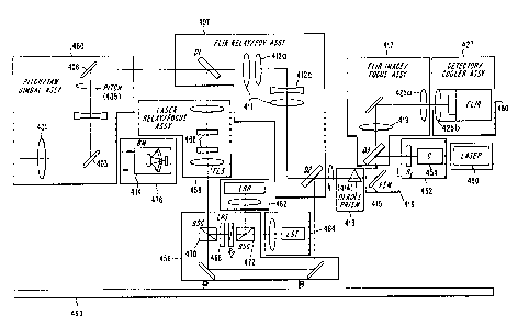
In a preferred embodiment of the present invention, as
illustrated in FIG. 4, IR energy enters a segmented target
CA 02342413 2001-04-23
-11-
acquisition window (not shown), and is collected by a common
pitch/yaw gimbal afocal 401. The common pitch/yaw gimbal
afocal 401, or common aperture, is referred to as "common"
because the same aperture is utilized to transmit and/or
receive IR energy as well as laser energy. The common
aperture 401 is actually a set of lenses comprising one
positive lens 401a and two negative lenses 401b and 401c, as
illustrated in FIG. 5A. This set of lenses equalizes the
index of refraction for both the IR energy and the laser
energy, thereby making it feasible to utilize a single
aperture for both the laser energy and IR energy. Having a
single aperture for both the laser energy and the IR energy
significantly reduces both fixed and dynamic alignment
errors between the FLIR LOS and the laser LOS.
The common aperture 401 reduces the diameter of the IR
energy beam as it enters the system and directs it toward a
turning mirror 403. The turning mirror 403 then directs the
IR energy beam down the pitch-axis centerline 405. A
turning mirror 406 then redirects the laser energy and the
IR energy parallel to the system longitudinal axis where it
encounters a Dichroic Dl located within the FLIR relay/FOV
assembly 407. Dichroic D1 separates the incoming energy
based on spectral content. Dichroic D1 accomplishes this by
transmitting energy'having wavelengths that are greater than
-2.7 microns (e. g., IR energy) and reflecting energy having
wavelengths that are shorter than -.2.0 microns (e. g., laser
energy) .
The FLIR Relay/FOV assembly 407 contains a number of
fixed lenses 411a and 411b, and a number of movable lenses
412a and 412b. These lenses act upon the IR energy so as to
decrease or increase the IR beam diameter depending upon
whether the FLIR relay/FOV assembly 407 is in the narrow FOV
(NFOV) mode or the wide FOV (WFOV) mode, respectively, as
will be explained in greater detail below. The IR energy
then passes through a dichroic D2 which transmits the IR
energy in the same manner as dichroic D1.
CA 02342413 2001-04-23
-12-
The IR energy next encounters a deroll assembly 413.
The deroll assembly 413 includes a deroll prism 414 and a
servo motor (not shown) for rotating the deroll prism 414.
The deroll prism 414 internally reflects the IR beam an odd
number of times, for example, three times, and causes the IR
energy to exit the deroll prism 414 in the same direction
that it entered the deroll prism 414. When the deroll prism
414 is rotated by the servo motor, about an axis defined by
the IR optical beam, it has the effect of counter-rotating
the FLIR image at a 2:1 ratio (e. g., +22.5 degrees of deroll
prism 414 rotation results in -45 degrees of IR image
rotation) to counter the rotation of the FLIR image caused
by changes in pitch angle, as explained above. This is
referred to as the doubling-effect. The deroll prism 414
will be described in greater detail below.
A fast steering mirror (FSM) 415, contained within a
FSM assembly 416, then reflects the IR energy beam through a
dichroic D3 located in the FLIR imager/focus assembly 417.
The FSM 415 is used for fine LOS stabilization and removal
of motion induced image blur associated with gimbal scanning
and ground rush optical flow. The FSM 415 will also be
described in greater detail below.
The FLIR imager/focus assembly 417 includes an imager
afocal 419 which translates along linear bearings to
compensate for variations in focus over variations in
temperature and altitude. Thus, the imager afocal 419 is
capable of adjusting the focus of the IR energy over a range
of temperatures and altitudes.
The FLIR imager/focus assembly 417 is connected to the
FLIR detector/cooler assembly 427. To facilitate FLIR
detection and imaging, the lens set comprising lenses 425a
and 425b collimates the IR energy as it passes through the
FLIR imager/focus assembly, FLIR detector/cooler assembly
interface. By collimating the IR energy, the IR image is
far less sensitive to small alignment errors between the
CA 02342413 2001-04-23
-13-
FLIR imager/focus assembly 417 and the FLIR detector/cooler
assembly 427.
As previously mentioned, the FLIR relay/FOV assembly
407 provides both a NFOV and a WFOV for the area of
interest. In the NFOV mode, the FLIR relay/FOV assembly 407
employs a first set of lenses 501 and a second set of lenses
502, as illustrated in FIG. 5A. Note, the first lens set
501 and the second lens set 502 appear as single lenses 411a
and 411b in FIG. 4. Both the first lens set 501 and the
second lens set 502 represent achromatic doublets (i.e., a
positive and a negative lens pair), and they are both fixed
with respect to the IR optical path. Individually, the
first lens set 501 focuses the IR energy; the second lens
set 502 recollimates the IR energy. Together, the first
lens set 501 and the second lens set 502 provide a maximum
afocal magnification and hence, a minimum FOV. Note there
are no moving optical elements in the FLIR Relay/FOV
assembly 407 when in the NFOV mode. Optical elements that
move are more likely to cause alignment errors, and in the
NFOV, boresight retention and integrity are at their most
critical.
In the WFOV mode, the FLIR relay/FOV assembly 407
employs the first lens set 501 and the second lens set 502,
described above, as~well as a single lens 412a and a third
lens set 504, as illustrated in FIG. 5B. Again, it should
be noted that the third lens set 504 appears as a single
lens 412b in FIG. 4. Unlike the first lens set 501 and the
second lens set 502, the single lens 412a and the third lens
set 504 are not fixed with respect to the FLIR optical path.
Instead, they are rotated into the FLIR optical path when
the FLIR relay/FOV assembly 407 transitions to the WFOV mode
and out of the FLIR optical path when the FLIR relay/FOV
assembly 407 transitions back to the NFOV mode. The single
lens 412a and the third lens set 504 are rotated into and
out of the FLIR optical path by a WFOV switch (not shown).
The single lens 412a and the third lens set 504, along with
CA 02342413 2001-04-23
-14-
the fixed lenses described above, produce a minimum afocal
magnification resulting in a large FOV.
Both the fixed lenses and the rotating lenses are
located about an intermediate focal plane along the IR
optical path such that a real entrance pupil and a real exit
pupil are generated in both the NFOV mode and the WFOV mode.
This, in turn, permits the IR energy to pass through the
same common aperture 401 in the pitch/yaw gimbal assembly
460 whether the system is operating in the NFOV mode or the
WFOV mode without effecting the less than 2.0 micron
wavelength functions.
FIG. 4 also shows the optical path for the laser
energy. During the transmission of laser energy, collimated
laser energy exits the laser transmitter 450 and enters the
compensator assembly 452. The compensator assembly contains
a compensator unit 454 and a pair of Risley prisms R1. The
compensator unit 454 adjusts the phase relationship between
orthogonal polarization states of the incident laser beam,
the purpose of which is to ensure that a sufficient amount
of laser energy is transmitted through the beam splitting
cube 470 as the deroll prism 414 is rotated as explained
above. Collimated laser energy then passes from the
compensator unit 454 through the Risley prisms R1, which are
used to steer the laser LOS. The compensator assembly 452
will be described in greater detail below.
The laser energy exits the compensator assembly 452 and
is reflected by Dichroic D3 towards the FSM 415. As
explained above, the FSM 415 minimizes fitter of both the
laser LOS and the FLIR LOS, further helping to ensure that
the laser energy is accurately directed to the desired
target.
The laser energy then passes into the deroll prism 414,
where it is internally reflected as was the IR energy as
explained above. After exiting the deroll prism 414, the
laser energy is reflected by dichroic D2 through the
combined optics assembly (COA) 456 and the laser relay/focus
CA 02342413 2001-04-23
-15-
assembly 458. Eventually, the laser energy encounters
dichroic D1, which reflects the laser energy into the
pitch/yaw gimbal assembly 460, which in turn directs the
laser energy along a common pitch axis, through the common
aperture 401, and in the direction of the desired target.
Laser energy returning from the desired target enters
the sensor through the segmented window Cnot shown) before
passing through the common aperture 401. It then follows
the same optical path as the IR energy (i.e., along a common
pitch axis) until reaching D1, which reflects the laser
energy through the laser Relay/focus assembly 458 and into
the COA 456. The COA 456 then redirects the return laser
energy into either the laser range receiver (LRR) 462 or the
laser spot tracker (LST) 464 depending on the state of the
LST/LRR switch (LRS) 466.
The laser subsystem components including the laser
transmitter 450, the compensator assembly 452, the COA 456,
the LRR 462, the LST 464, and the laser relay/focus assembly
458 will now be described in greater detail.
In a preferred embodiment, the laser transmitter 450 is
a diode-pumped solid state ND:YAG laser. Diode pumped
transmitters are preferable over flashlamp pumped lasers
with the same optical output power because diode pumped
transmitters are more reliable, require less power, and have
longer life spans. The laser transmitter 450 uses an
optical parametric oscillator to generate a 1.57 micron
training wavelength in addition to a 1.064 micron tactical
wavelength. It is possible to obtain components so that the
output of the laser transmitter 450 has a beam quality
(i.e., brightness) of better than 9 mm-mrad measured at the
laser output port and is also capable of transmitting
greater than 90 mJ at 1.064 microns and 26 mJ at 1.57
microns. Moreover, the laser transmitter output is driven
by a Pulse Inter-Period Modulation (PIM) code or at a pulse
repetition frequency (PRF) of up to 20 Hz, with a pulse
width of 20 nanoseconds.
CA 02342413 2001-04-23
-16-
The LRR 462 consists of a low noise InGaAs receiver
responsive to both the 1.064 micron tactical wavelength and
the 1.57 micron training wavelength. The LRR 462 is
remotely located from the laser and uses a low level
backscatter of the outgoing laser pulse as a trigger for its
timing circuitry. The LRR 462 is remotely located from the
laser transmitter 450 and polarization isolated by the COA
456 to prevent the outgoing laser energy from specullarly
reflecting into the LRR 462. The energy level of the
outgoing laser pulse is many orders of magnitude higher than
the energy level of the return laser pulse. And, if the
energy of the outgoing laser pulse, or even a very small
percentage of the outgoing laser energy, reflects into the
LRR 462, the LRR will become saturated and incapable of
detecting the return pulses in time. The LRR 462 is capable
of ranging from about 0.25 nautical miles to greater than
about 20 nautical miles at an accuracy of +/- 3 meters.
In a preferred embodiment of the present invention, the
LST 464 uses a quad cell silicon detector to acquire laser
spot tracks.
The laser relay/focus assembly 458 provides two
functions. First, it optically relays the transmitted and
received laser energy between dichroic D1 and the COA 456.
Second, it maintains laser energy focus over temperature and
altitude by translating a set of focus lenses FL3. The
laser relay/focus assembly 458 translates the focus lens set
FL3 along linear bearings using a motor driven lead screw
and by monitoring position feedback with a potentiometer.
Laser energy is actually focused inside a vacuum cell (not
shown) that~is built~into the laser relay/focus assembly
housing. The laser energy passes into and out of the vacuum
cell through a set of vacuum cell windows 468.
The compensator assembly 452, as stated above, contains
a pair of Risley prisms R1 and a compensator unit 454, and
it performs three primary functions. First, the compensator
assembly 452 is capable of shifting the laser LOS to adjust
CA 02342413 2001-04-23
-17-
the laser-to-FLIR boresight. Second, the compensator
assembly 452 is capable of adjusting the polarization of the
laser energy in order to compensate for perturbations
introduced by the deroll prism 414. Third, the compensator
assembly is capable of adjusting the polarization of the
laser energy so as to alternate the intensity of the laser
energy during the internal boresighting procedure as will be
explained in greater detail below. Tasks are accomplished
by the compensator unit 454.
As illustrated in FIG. 6, the compensator unit 454
contains two optical waveplates, a a/4 waveplate 605 and a
~/2 waveplate 610, which are individually rotated as a
function of deroll angle (i.e., the angle of the deroll
prism 414), under the control of a microprocessor-based
circuit (not shown) which monitors deroll angle. Both the
~/4 waveplate 605 and the ~/2 waveplate 610 are individually
mounted in an identical ball-bearing-supported, gear-driven
housing, and each has its own drive mechanism composed of a
servo motor and a position feedback resolver.
FIG. 6 illustrates that an outgoing laser beam 615 is
linearly polarized when it leaves the laser transmitter 450.
However, to ensure that the laser beam is linearly polarized
when it exits the deroll prism 414, the ~/4 waveplate 605
can be rotated to vary the ellipticity of the laser beam
polarization, and the ~/2 waveplate 610 can be rotated to,
in turn, rotate the orientation of the ellipse. By ensuring
that the laser beam is linearly polarized when it exits the
deroll prism 414, the laser beam will be linearly polarized
when it passes through the polarizing beam splitter cube
470, thus ensuring that the energy level of the transmitted
laser beam will be sufficient to illuminate the desired
target. It is important to note, that the order in which
the laser beam encounters the ~/4 waveplate 605 and the ~/2
waveplate 610 is important.
The COA 456 is an electromechanical/optomechanical
assembly that redirects the return laser energy beam into
CA 02342413 2001-04-23
-18-
the LRR 462 or the LST 464. The COA 456 also helps to
maintain a proper laser-to-LRR boresight and a proper laser-
to-LST boresight.
When the laser energy returns to the system from the
desired target, it is randomly polarized. In the COA 456,
the randomly polarized laser energy is redirected into a a/2
waveplate 466 by a polarizing beamsplitter 470. In the
preferred embodiment, the ~/2 waveplate 466 rotates the
polarization of the laser energy such that the laser energy
is adjusted for the LRR detector, the LST detector, or
divided between the same. Thus, the ~/2 waveplate 466
serves as an LRR/LST switch.
After the ~/2 waveplate 466 polarizes the laser energy,
a pair of Risley prisms R2, the same as the pair of Risley
prisms R1, is employed to shift the laser LOS within the COA
456, thereby adjusting the laser-to-LRR or the laser-to-LST
boresight. Both the Risley pair R1 and the ~/2 waveplate
466 have their own drive mechanisms comprising a servo motor
and a position feedback resolver.
After passing through the pair of Risley prisms R2, the
laser energy encounters a polarizing beamsplitter 472. The
polarizing beamsplitter 472 redirects the laser energy into
the LRR 462, the LST 464, or both depending upon the
rotation state of the ~/2 waveplate 466 (i.e., the LRR/LST
switch).
In order to stabilize, correct and control the laser
LOS and the FLIR LOS, the present invention employs a
LOS/servo subsystem. The LOS/servo subsystem helps to
minimize dynamic fitter for both the FLIR LOS and laser LOS.
FIG. 7 is a diagram of the LOS/servo subsystem, which
includes a six-axis gimbal assembly 705, a number of single,
dual and three phase servo motors 710, power amplifiers 715,
various rate and position sensors 720, a digital interface
725, and a digital processor 730.
The six-axis gimbal assembly 705 includes the pitch/yaw
gimbal assembly 460, a roll gimbal (not shown), the deroll
CA 02342413 2001-04-23
-~. .-
-19-
assembly 413, and the FSM 415. The pitch/yaw gimbal
assembly 460, the deroll assembly 413, and the FSM 415 are
all mounted on a passively isolated optical bed 490 that is
supported by the roll gimbal. The isolated optical bed 490
attenuates high-frequency vibrations and minimizes
structural bending (i.e., low to mid frequency vibrations),
all of which might significantly contribute to LOS and
dynamic alignment errors.
The pitch/yaw gimbal assembly 460, in turn, comprises
an inner gimbal (i.e., a yaw gimbal) that includes a set of
lenses 401a, 401b and 401c, as illustrated in FIG. 5A and 8,
and a gimbaled mirror 403. Note, the lens set comprising
lenses 401a, 401b and 401c is shown as a single lens 401 in
FIG. 4. Lenses 401a, 401b and 401c are the optical elements
which make up the common pitch/yaw afocal (i.e., the common
aperture mentioned above). The inner gimbal provides
limited rotational movement about the yaw axis
(approximately 5 degrees). The pitch/yaw gimbal assembly
460 also has an outer gimbal (i.e., a pitch gimbal), which
contains a fourth lens 815. The outer gimbal provides a
full 360° of rotation about the pitch axis 405. In
addition, there is only one pitch axis interface between the
pitch/yaw gimbal assembly 460 and the host platform, and
therefore, a common~set of pitch bearings for the laser
optics and for the FLIR optics. The pitch/yaw gimbal
assembly 460 utilizes two separate servo motors (not shown).
The roll gimbal and the deroll assembly 413 provide LOS
pointing and image roll stabilization respectively. More
specifically, the deroll assembly 413 provides fine roll
stabilization and horizontal stabilization for the FLIR
image as the system rotates about the roll axis and/or the
gimbal assembly rotates about the pitch axis. Image deroll
is actually accomplished by a deroll prism 414, mounted in a
cylindrical housing that rotates on low-friction, preloaded,
duplex bearings. The rotating assembly is driven by a
direct-drive, pancake torque motor and position is sensed
CA 02342413 2001-04-23
-20-
through a pancake resolver, mounted coaxially with the
motor.
The FSM assembly 416 is comprised of position probe
electronics 930 and the electromechanical assembly 900. The
FSM electromechanical assembly 900 is an electromechanical
device which rotates a FSM 415 about the pitch axis 910 and
the yaw axis 915 as illustrated in FIG. 9 (see also, U.S.
Patent No. 5,550,669). In a preferred embodiment, the FSM
900 provides fine stabilization for the FLIR LOS and the
laser LOS. This is accomplished by measuring the pitch and
yaw gimbal motion with the IMU 720 and by applying a
position correction command to the FSM position servo motors
917. The FSM servo motor position commands are, in turn,
controlled by a FSM servo electronics assembly 920. FSM
position feedback is provided by a set of position probes
925 and a position probe electronics assembly 930.
The LOS control sensors 720 provide digital information
to the LOS control software residing in the LOS control
processor 730. The LOS control processor generates LOS
control signals to control both the FLIR LOS and the laser
LOS. The LOS control sensors 720 include an angular roll
rate sensor which provides digital roll rate information;
resolvers which provide gimbal angle position; position
probes which provide position information for the FSM 415;
and an inertial measurement unit (IMU) assembly (not shown).
The IMU assembly is comprised of a three-axis fiber-optic
gyro (FOG) and a three-axis accelerometer. The IMU provides
incremental angle information, as a function of inertial
angular rate, and incremental velocity information, as a
function of inertial linear acceleration.
While the LOS servo subsystem helps to minimize dynamic
alignment errors, the present invention contains an internal
boresight module (BM) 474, to minimize fixed alignment
errors between the various internal lines of sight, as
illustrated in FIG. 4. The BM 474 is optically connected to
the pitch/yaw gimbal assembly 460 and, along with a
CA 02342413 2001-04-23
-21-
boresight control algorithm, is used for aligning the
internal lines of sight with respect to each other. The
internal lines of sight include the FLIR NFOV LOS, the FLIR
WFOV LOS, the laser transmitter LOS, the LRR LOS, and the
LST LOS.
FIG. 10 shows the BM 474 in greater detail. The BM
474, which is contained inside a housing 476, includes an
aperture window 1005 through which IR and laser energy pass.
The BM 474 also contains a Cassegrain optical system,
including a primary and a set of secondary mirrors 1006 and
1007 respectively, for directing the IR and laser energy
into and out of the BM 474. In addition, the BM 474
includes a reticle 1010; a laser filter 1025, which prevents
laser energy from passing through certain openings in the
reticle 1010; an IR/visible light source 1015; a laser
detector 1020; and a laser source 1030.
During the FLIR LOS alignment procedure, described in
greater detail below, the IR/visible light source 1015 emits
both IR energy and visible light energy, which pass through
a diffuser 1016, a dichroic 1017, and an optical lens 1018.
The energy then reflects off of a second dichroic 1019,
through the reticle 1010, wherein it is directed out of the
BM 474 by the primary and secondary mirrors 1006 and 1007.
During the laser LOS alignment procedure, described in
greater detail below, laser energy from the laser
transmitter 450 is directed into the BM 474 by the primary
and secondary mirrors 1006 and 1007. The laser energy then
passes through the reticle 1010 and into the laser detector
1020 via the dichroic 1019 and an optical lens 1024.
During the LRR and the LST boresight procedure, the
laser source 1030 emits laser energy, which passes through
an optical lens 1031. The laser energy then reflects off of
the dichroic 1017, passes through the optical lens 1018,
reflects off of the second dichroic 1019, passes through the
reticle 1010 and out of the BM 474. In a preferred
CA 02342413 2001-04-23
-22-
embodiment, the laser source 1030 is a laser emitting diode
(LED) .
The reticle 1010 contains a reticle pattern 1100, as
illustrated in FIG. 11. The reticle pattern 1100, includes
a number of unusually shaped openings, through which either
laser or IR energy pass during the various LOS alignment
processes. As shown in FIG. 11, the various openings are
symmetrically arranged around a 1064 microradian circular
region. At the very center of this circular region is a 60
microradian hole, which is coincident with the center of the
reticle pattern 1100.
The first set of openings in the reticle pattern 1100
include five octagonal shaped openings 1105a-e. These
openings allow IR energy to pass through the reticle 1010
during the FLIR LOS alignment procedure. As will be
explained below, the first four openings 1105a-d are used
for symmetrically aligning the FLIR LOS with respect to the
center of the FLIR focal plane array. The fifth opening
1105e is used for rotationally aligning the FLIR LOS with
respect to the FLIR focal plane array.
The reticle pattern 1100 also has a number of
checkerboard-like openings 1110. The checkerboard-like
openings are used in conjunction with special signal
processing software'. This software, in turn, controls the
procedure for focusing the FLIR image prior to the FLIR
alignment process. The larger checkerboard-like openings
are specifically used for focusing the WFOV FLIR image,
while the smaller checkerboard-like openings are used for
focusing the NFOV FLIR image. The signal processing
software which utilizes the checkerboard-like openings will
be described in more detail below.
Finally, the reticle pattern 1100 contains four wedge
shaped openings 1115. Unlike the octagonal shaped openings
described above, the wedge shaped openings 1115 allow laser
energy from the laser transmitter 450 to pass through the
reticle 1010 during the laser LOS alignment procedure.
CA 02342413 2001-04-23
-23-
The method for boresighting the FLIR LOS, the laser
transmitter LOS, then LRR LOS and the LST LOS will now be
described in greater detail hereinbelow with reference to
FIG. 12. To begin, a boresight command is generated in
accordance with block 1205. The pitch gimbal then rotates
165° as shown in block 1210. By rotating the pitch gimbal
165 degrees, the BM 474 becomes an integral part of the FLIR
optical path and the laser optical path. Next, the signal
processing routines that control the servo motors which, in
turn, move the various IR and laser optics during the
boresight procedure are activated in accordance with block
1215. The NFOV FLIR image and the WFOV FLIR image are then
brought to focus on the focal plane array 480 in the FLIR
detector/cooler assembly 427, in accordance with blocks 1220
and 1225 respectively. The FLIR LOS alignment procedure
begins once the NFOV and the WFOV FLIR images are focused,
in accordance with block 1230. The FLIR LOS is aligned with
the center of the focal plane array 480 using the IR/visible
light source 1015, the reticle pattern 1100 and, more
specifically, the octagonal shaped openings 1105a-a in the
reticle pattern 1100 as described above. The FLIR LOS
alignment procedure is specifically accomplished by first
illuminating the IR/visible light source 1015. The IR and
visible light energy~pass through the five octagonal shaped
openings 1105a-a in the reticle pattern 1100. The energy
passing through each of the five octagonal shaped openings
1105a-a will cause five corresponding regions on the focal
plane array 480 to become illuminated. With the roll servo
locked, the signal processing routines mentioned above
command the pitch and yaw servos to, in turn, rotate the
pitch and yaw gimbals until the first four illuminated
regions on the focal plane array 480, corresponding to the
first four octagonal shaped openings 1105a-d, are
symmetrically located about the center of the focal plane
array 480. Then, with the pitch and yaw servos holding
their positions, the signal processing routines and the
CA 02342413 2001-04-23
-24-
deroll servo use the fifth illuminated region on the focal
plane array 480, corresponding to the fifth octagonal shaped
opening 1105e, to perform a roll alignment of the reticle
pattern 1100 with respect to the focal plane array 480, thus
completing the alignment of the FLIR LOS to the BSM.
Once the FLIR LOS is aligned, the laser LOS is aligned
as illustrated by block 1235. To align the laser LOS, the
laser transmitter 450 begins generating a continuous stream
of pulses at a nominal rate of 20 Hz. As explained above,
the laser filter 1025 only allows the laser energy from the
laser transmitter 450 to pass through certain openings in
the reticle pattern 1100, specifically, the 60° wedge shaped
openings 1115 and the 60 microradian hole at the center of
the reticle pattern 1100. When the laser transmitter 450
begins transmitting, the laser spot may not coincide with
one of the four wedge shaped openings 1115, as illustrated
by position 1305 in FIG. 13. In order to align the laser
spot with one of the four wedge shaped openings 1115, the
boresight algorithm commands the pair of Risley prisms R1 to
move the laser spot into different positions within a search
pattern 1310. Eventually, the laser spot will coincide with
one of the wedge shaped openings 1115, as illustrated by
position 1315. This will result in a detection by the laser
detector 1020. Next, the boresight algorithm commands the
Risley pair R1 to move the laser spot to the nearest radial
edge of the corresponding wedge shaped opening, as
illustrated by position 1320. Based upon the angle of the
radial edge, the boresight algorithm.can determine the
direction in which the laser spot must move in order to
reach the 60 microradian hole at the center of the reticle
pattern 1100. In FIG. 13, the direction of movement of the
laser spot is illustrated by the laser spot positions 1320,
1325 and 1330 in sequence.
When the laser spot reaches the inner edge of the
corresponding wedge shaped opening, it will be approximately
500 microradians from the center of the reticle pattern
CA 02342413 2001-04-23
-25-
1100. The boresight algorithm then commands the Risley pair
R1 to move the laser spot to a number of grid positions in
accordance with one of a number of possible rectangular grid
patterns, as illustrated in FIGS. 14A through 14F, wherein
each rectangular grid pattern encompasses a portion of the
1064 microradian circular region at the center of the
reticle pattern 1100, including the 60 microradian hole at
the very center. The particular grid pattern used will
depend upon the angle of the radial edge which was used as a
guide to move the laser spot toward the center of the
reticle pattern 1100. In the example above, the laser spot
traveled toward the center of the reticle along the lower
edge of the wedge shaped opening 1350, such that when the
laser spot reached the inner edge of the wedge-shaped
opening 1350, it was located at a position 1405 as
illustrated in FIG. 14A. Consequently, the rectangular grid
pattern illustrated in FIG. 14A will be used as a guide to
fine-tune the alignment of the laser spot with respect to
the center of the reticle pattern 1100.
Before the Risley pair R1 moves the laser spot to each
of the grid pattern positions associated with, for example,
the grid pattern shown in FIG. 14A, the boresight algorithm
commands the polarization compensator 454 to attenuate the
amount of laser energy being transmitted into the BSM. The
laser energy is attenuated to prevent the focused laser
energy from damaging the reticle and to adjust the energy
level so it lies in a range which is detectable by the laser
detector 1020. After attenuating the laser energy, the
Risley pair.Rl then moves the laser spot to each grid
pattern position. The position corresponding to the maximum
laser energy detection, as detected by the laser detector
1020, will be identified as the best laser LOS boresight
alignment position.
The image illuminated on the focal plane array 480 is
then rotated 180 degrees, in accordance with block 1237.
This is accomplished by rotating the deroll prism 90
CA 02342413 2001-04-23
-26-
degrees. The FLIR LOS alignment procedure, according to
blocks 1230, and the laser LOS alignment procedure,
according to block 1235, are then repeated. By repeating
these procedures, the boresight algorithm calibrates out any
alignment errors between the FLIR LOS and the laser LOS due
to the fact the IR energy and the laser energy travel along
partially different optical paths.
Since the IR energy passes through the octagonal
openings 1105, which are, in turn, symmetrically positioned
around the 60 microradian hole at the center of the reticle
pattern 1100, the alignment of the laser LOS to the 60
microradian hole results in a precise alignment between the
FLIR LOS and the laser LOS. The laser LOS to FLIR LOS
boresight algorithm described above is accurate to within 42
microradians with a laser beam divergence of 120
microradians or less.
Finally, the LRR 462 and the LST 464 are aligned in
accordance with blocks 1240 and 1245 respectively. To align
the LRR 462 and the LST 464, the laser transmitter 450 is
turned off and the laser diode 1030 is turned on. The laser
energy emitted by the laser diode 1030 is transmitted
through the 60 microradian hole located at the center of the
reticle pattern 1100. The energy from the laser diode 1030
then passes along the laser optical path, and into the COA
456. The COA 456 then directs the laser energy into the LRR
462. The LRR LOS is aligned by rotating the pair of Risley
prisms 466. The COA 456 then directs the laser energy into
the LST 464 and the LST LOS is similarly aligned.
In an alternative embodiment, as illustrated in FIG.
15, the elect-ro-optical subsystem employs a combined LST/LRR
assembly 1505. When the LST and the LRR are part of one
combined unit, there is no longer any need to alternately
direct laser return energy into the LRR and the LST.
Therefore, in the alternative embodiment the COA 456 is
greatly simplified. More specifically, LRR/LST switch 466,
BSC 472, and two mirrors are removed thereby reducing the
__. CA 02342413 2001-04-23
-27-
complexity of the COA 456. In addition, by combining the
LRR and the LST, there is no longer a need to separately
boresight the LRR and the LST. Also, by combining the LRR
and the LST, and by eliminating the LRR/LST switch 466, the
BSC 472, and the two aforementioned mirrors, there is
additional space available for a television camera 1510,
which can be used for presenting a near IR image of the AOI.
FIG. 16 shows the configuration of the combined LRR/LST
assembly 1505. The LST is preferably a quad-cell,
photosensitive device, wherein each cell outputs an
electrical signal 1605a through 1605d each being
proportional to the amount of laser energy illuminating the
corresponding cell. Quad-cell LSTs are generally well known
by those of ordinary skill in the art. The LRR 1610 is a
pin diode positioned directly in the center of the quad-cell
device, at the intersection of two high-impedance buffer
regions 1615a and 1615b, which electrically isolate the
quad-cells from each other. The LST quad cell with the
integrated LRR pin diode are housed within a hybrid. Pre-
and post-amplification circuitry for both the LST and LRR
sensors are co-located within this hybrid.
SEGMENTED WINDOW & EMI GRID
In a preferred embodiment, the opto-electric subsystem
described above is housed inside a pod assembly, the forward
portion of which (i.e., the shroud? is illustrated in FIG.
17. The pod assembly is connected to the host platform.
For example, the pod assembly may be suspended from a pylon
on the wing of a tactical aircraft such as an F-15, F-16, or
an F-18. While the shroud assembly physically protects the
opto-electronic equipment described above, laser energy and
IR energy pass into and out of the shroud assembly through a
segmented window 1705.
The window has four segments or panels, 1705a through
1705d. The segments are designed to optimize the aero-
optical performance of the system. For example, these
CA 02342413 2001-04-23
-28-
segments or panels reduce or prevent energy from reflecting
back into the opto-electronic sensor described above. Also,
the panels optimize the modular transfer function (MTF)
versus gimbal angle at the mission critical pitch angles of
0° and 20° at 20,000 AGL. Furthermore, the window panels
also support sensor scanning from +35° to -155° in pitch.
360° in roll and t 5° yaw. In addition, the segmented
window is employed in lieu of a shroud follower, which
requires more hardware and exhibits a larger radar cross-
IO section (RCS) and aerodynamic drag coefficients.
The four window panels consist of a substrate material
and three required coatings: an electromagnetic interference
coating, a durable anti-reflection (DAR) coating, and an
interior anti-reflection (IAR) coating. A number of
different materials could be used for the substrate. For
example; "Cleartran" (multi-spectral ZnS) is commonly used
for this purpose. While exhibiting good multispectral
characteristics, it is not very durable. In contrast,
sapphire is very durable and it exhibits good transmissivity
characteristics in the midwave range (i.e., ~3-4.5 microns).
Therefore, in a preferred embodiment, sapphire is used for
the substrate material.
Each of the aforementioned panels also contain an EMI
grid. In general, the EMI grid reduces the exposure of the
sensor and the sensor electronics to large EM fields which
may be present in an operational environment. For example,
the EMI grid may be used to minimize or eliminate EM energy
effects on the system electronics (e. g., the IMU, FLIR
analog electronics, FSM probes), which are susceptible to
this type of radiation, emanating from sources (i.e., radar)
located on the host platform (e. g., F-16, F-18). The grid
may also minimize EM energy from the electronics located
within the pod assembly which could adversely effect
electronics located on the host platform.
In general, EMI grids are well known to those of skill
in the art. However, prior EMI grids employ square or polar
CA 02342413 2001-04-23
i
-29-
(concentric) patterns. These prior EMI grid patterns
generate unacceptable artifacts on the FLIR image. For
example, a square grid pattern concentrates energy along
four lines radiating from the off-axis light source and
often produces an energy artifact 1800 as illustrated in
FIG. 18. This energy appears on the FLIR image as
illustrated and is unacceptable.
In a preferred embodiment, an EMI grid pattern
comprising an array of circles is employed as illustrated in
FIG. 19. This EMI grid pattern conducts or diffracts stray
light energy radially, rather than along specific axes, thus
reducing or eliminating unwanted light energy artifacts on
the FLIR image. In the arrangement of FIG. 19, each circle
preferably has a line width of 5 micrometers and a diameter
of 320 micrometers. The repetition offset (i.e., the
distance between the center of two adjacent circles) is 315
micrometers where there is a 100 percent overlap of the
circular lines at the circle tangent points.
The specific EMI grid dimensions described above
represent but one exemplary embodiment of the EMI grid.
Those of ordinary skill in the art will appreciate that
other dimensions may be employed without exceeding the
intended scope of the EMI grid pattern described above.
The EMI grid of the present invention is attached to
the segmented window panels in much the same way as in the
prior art. First, three metal layers are applied to the
window: an inner adhesion layer, a middle conduction layer,
and an outer protection layer. Different metals may be used
for each layer; however, chrome is typically used for the
inner layer, gold for the middle layer, and titanium for the
outer layer. A "mask" is placed over the window material,
and then exposed to ultraviolet light. The ultraviolet
light removes the metal layers from those areas not
protected by the mask. When the mask is removed, the EMI
grid is affixed to the window.
_ CA 02342413 2001-04-23
-30-
FAULT ISOLATION
The electro-optics subsystem comprises a number of
servo systems. Each servo system contains one or more
amplifiers and a single, dual or three phase servo motor.
These servo systems provide the power and the mechanical
force necessary to rotate and/or translate various lenses,
prisms, mirrors, and waveplates in the electro-optics
subsystem. The servo systems include a dual-phase,
brushless DC motor and pulse width modulated (PWM) amplifier
servo systems (i.e., the pitch servo system and the deroll
servo system). Also included is a three-phase, brushless DC
motor, PWM amplifier servo system (i.e., the roll servo
system). Further included are several single-phase motor,
linear amplifier servo systems (i.e., the various laser and
FLIR focusing assembly servo systems, the thermal reference
servo system, the FSM servo system, the risley prism servo
systems, the yaw servo system, and the control, inlet, and
exit airflow servo systems).
In order to detect the existence of fault conditions in
any one of the above-identified servo systems, the present
invention provides a fault isolation capability that can
determine whether the fault conditions have occurred in the
amplifier portion of a given servo system or in the motor
portion of the given servo system. By isolating a fault to
the amplifier portion or the motor portion of the given
servo system, the need to remove and/or replace the entire
servo system is avoided. Instead, only the amplifier or
motor portion containing the fault condition need be removed
and/or replaced. Prior art has required test loads and a
means for switching the loads in and out of circuit. This
technique does not require test loads.
FIG. 20 is a diagram of a dual-phase, brushless DC
motor, PWM amplifier servo system circuit 2000. Under
ordinary conditions, the circuit 2000 controls the
commutation of the current through the windings of the dual
phase motor M, which in turn control the rotation of the
_ CA 02342413 2001-04-23
-31-
motor shaft. More particularly, the dual-phase, brushless
DC motor, PWM amplifier servo system circuit 2000 comprises
two PWM amplifiers A and B. Each of these amplifiers A and
B has two upper drive transistors T1 and T2, and two lower
drive transistors T3 and T4. To commutate the current
through the motor windings thus causing the shaft of the
dual-phase motor M to rotate, one skilled in the art will
readily understand that it is necessary to pair the upper
drive transistors in each amplifier with the lower drive
transistor located on the other side of the same amplifier.
For example, in amplifier A, transistor T1 will be paired
with transistor T4, and transistor T2 will be paired with
transistor T3. Similarly, in amplifier B, transistor T1
will be paired with transistor T4 and transistor T2 will be
paired with transistor T3. Then, by alternately activating
each pair of drive transistors (a technique known as
complimentary switching), first in amplifier A and then in
amplifier B, the dual-phase motor, PWM amplifier servo
system circuit 2000 can maintain a constant torque on the
shaf t of motor M .
The dual-phase motor, PWM amplifier servo system
circuit 2000 also includes a control circuit 2005. The
control circuit 2005 specifically controls the timing of the
complementary switching process (i.e., when each drive
transistor pair is activated) to control load current using
a standard feedback configuration. In the present
invention, the control circuit 2005 is implemented with a
field programmable gate array (FPGA); however, one skilled
in the art will readily understand that the control circuit
2005 can be implemented using other forms of logic without
departing from the spirit of the invention.
In addition, each amplifier A and B, in the dual-phase
motor, PWM amplifier servo system circuit 2000, contains two
upper current sensing resistors R1 and R2. The upper
current sensing resistors R1 and R2 monitor the amount of
current flowing through the upper drive transistors T1 and
CA 02342413 2001-04-23
-32-
T2 respectively. Furthermore, each amplifier A and B
contains a lower current sensing resistor Ro. The lower
current sensing resistor Ro is utilized for monitoring the
current flowing through the lower drive transistors T3 and
T4. It is important to note that in the present invention,
amplifiers A and B contain insulated gate bipolar
transistors (IGBTs). IGBTs are utilized, in part, because
their utilization simplifies the design of the control
circuit 2005, given a 270 volt source Vcc, as one skilled in
the art will readily understand. However, one skilled in
the art will also recognize that solid state switches such
as MOSFETs and bipolar transistors could be employed.
In general, the dual-phase, PWM amplifier servo system
fault isolation process works as follows. Complimentary
switching of transistor pairs is disabled. The control
circuitry 2005 activates a pair of drive transistors, for
example T1 and T4 in amplifier A. The control circuitry
2005 will then deactivate this drive transistor pair and, in
turn, activate and deactivate each of the other drive
transistor pairs: T2 and T3 in amplifier A, T1 and T4 in
amplifier B, and T2 and T3 in amplifier B. Under normal
operating conditions (i.e., when there is no fault condition
present), the activation of each drive transistor pair will
cause a specific amount of current to flow through the
corresponding upper current sensing resistor R1 or R2,
through the corresponding upper drive transistor T1 or T2,
through the corresponding servo motor winding, through the
corresponding lower drive transistor T3 or T4, and
eventually through the lower current sensing resistor Ro.
If, in fact, there are no fault conditions present, a known
voltage drop will always develop across the upper current
sensing resistor R1 or R2 and across the lower current
sensing resistor Ro. However, if a fault condition does
exist, the amount of current flowing through the upper
current sensing resistor R1 or R2, and/or across the lower
current sensing resistor Ro will be significantly affected.
CA 02342413 2001-04-23 _
-33-
By monitoring the amount of current flowing through these
resistors as each of the above-identified drive transistor
pairs is activated, the following single point fault
conditions can be isolated, as will be described in greater
detail below: motor winding short circuit, motor winding
open circuit, amplifier short circuit, motor winding short-
to-ground, amplifier open circuit.
FIG. 21 is a flowchart which depicts the steps of the
dual-phase motor, PWM amplifier fault isolation process, in
accordance with a preferred embodiment of the present
invention. In accordance with FIG. 21, the control circuit
2005 initiates the process by disabling the complementary
switching as illustrated by block 2101. Once the
complementary switching has been disabled, the control
circuit 2005 is free to activate and deactivate the drive
transistor pairs for the purpose of fault isolation.
After the complementary switching has been disabled,
the control circuit 2005 generates a positive current
command +I, as illustrated by block 2105. The positive
current command activates the transistor pair comprising
drive transistors Tl and T4. The control circuit 2005 then
determines whether the magnitude of the current flowing
through the upper current sensing resistor R1 is normal or
whether it exceeds a normal amount, i.e., whether it exceeds
a predetermined threshold value, as illustrated by decision
block 2110. If the magnitude of the current flowing through
the upper current sensing resistor R1 is excessive, in
accordance with the "YES" path out of decision block 2110,
the control circuit 2005 determines whether the magnitude of
the current flowing through the lower current sensing
resistor RO is equal to zero, as illustrated by decision
block 2112. If the current flowing through the lower
current sensing resistor RO is equal to zero, in accordance
with the "YES" path out of decision block 2112, the control
circuit 2005 will generate an amplifier SHUTDOWN command, as
illustrated in block 2113. Since the control circuit 2005
CA 02342413 2001-04-23
-34-
determined the amount of current to be zero, the fault
condition is identified as a motor winding short-to-ground,
as illustrated by block 2114. If the control circuit 2005
determines that the current flowing through the lower
current sensing resistor is not equal to zero, in accordance
with the "NO" path out of decision block 2112, control logic
2005 will nevertheless generate an amplifier SHUTDOWN
command, as illustrated by block 2115. However, it is still
undetermined whether the fault condition causing the
excessive amount of current through the upper current
sensing resistor R1 is due to a short circuit in the motor
winding or a short circuit in the amplifier. Therefore, the
control circuit then generates a negative current command-I,
as illustrated by block 2120, which activates the transistor
pair comprising drive transistors T2 and T3. The control
circuit 2005 now determines whether the magnitude of the
current flowing through the upper current sensing resistor
R2 is excessive, i.e., whether it exceeds the predetermined
threshold, as illustrated by decision block 2125. If the
amount of current flowing through the upper current sensing
resistor R2 does exceed the threshold value, in accordance
with the "YES" path out of decision block 2125, the control
circuit 2005 will, once again, generate an amplifier
SHUTDOWN command, a~s illustrated by block 2130. Since an
excessive amount of current is drawn through both upper
current resistors R1 and R2, the fault condition is
identified as a servo motor winding short circuit, as
illustrated by step 2135. If, however, the magnitude of the
current flowing through the upper current sensing resistor
R2 does not exceed the predetermined threshold value, in
accordance with the "NO" path out of decision block 2125,
i.e., if only one of the upper current sensing resistors
draws an excessive amount of current, the fault condition is
identified as an amplifier short circuit, as illustrated by
step 2140.
CA 02342413 2001-04-23
-35-
If, after generating the positive current command +I,
according to block 2105, the control circuit 2005 determines
that the magnitude of the current flowing through the upper
current sensing resistor R1 did not exceed the predetermined
threshold, in accordance with the "NO" path out of decision
block 2110, the control circuit 2005 then determines whether
the magnitude of the current flowing through the lower
current sensing resistor Ro is equal to zero, as illustrated
by decision block 2145. If the magnitude of the current
flowing through the lower current sensing resistor does
equal zero, the control circuit 2005 then generates a
negative current command -I, as illustrated by block 2150,
and determines whether the magnitude of the current flowing
through the upper current sensing resistor R2 exceeds the
predetermined threshold value, as illustrated by decision
block 2155. If the magnitude of the current flowing through
the upper current sensing resistor R2 exceeds the
predetermined threshold value, in accordance with the "YES"
path out of decision block 2155, the control circuit 2005
will generate an amplifier SHUTDOWN command, as illustrated
by block 2160. Since an excessive amount of current was
detected through only one of the upper current sensing
resistors, i.e., R2, the fault condition is identified as an
amplifier short circuit, as illustrated by step 2165.
If, however, the magnitude of the current flowing
through the upper current sensing resistor R2 does not
exceed the predetermined threshold value, in accordance with
the "NO" path out of decision block 2155, the control
circuit 2005 will determine whether the magnitude of the
current flowing through the lower current sensing resistor
is equal to zero, as illustrated by decision block 2170. If
the current flowing through the lower current sensing
resistor Ro does equal zero, i.e., both R1 and R2 drawing
normal amounts of current and Ro drawing no current when T1
and T4 are activated and when T2 and T3 are activated, the
fault condition will be identified as a motor winding open
_ CA 02342413 2001-04-23
-36-
circuit, as illustrated by step 2175. If the current
flowing through the lower current sensing resistor Ro does
not equal zero, in accordance with the "NO" path out of
decision block 2170, i.e., both Rl and R2 are drawing normal
amounts of current and Ro drawing no current only when T1
and T4 are activated, the fault condition is identified as
an amplifier open circuit, as illustrated by step 2180.
If, however, the magnitude of the current flowing
through the lower current sensing resistor Ro does not equal
zero, in accordance with the "NO" path out of decision block
2145, the control circuit 2005 will generate a negative
current command -I, as illustrated by block 2185, which
activates the transistor pair comprising drive transistors
T2 and T3. The control circuit 2005 then determines whether
the magnitude of the current flowing through the upper
current sensing resistor R2 exceeds the predetermined
threshold, as illustrated by decision block 2190. If the
magnitude of the current flowing through the upper current
sensing resistor R2 exceeds the threshold, in accordance
with the "YES" path out of decision block 2190, i.e., an
excessive amount of current is flowing through only one of
the upper current sensing resistors, the control circuit
2005 generates an amplifier SHUTDOWN command, as illustrated
by block 2160, and the fault condition is identified as an
amplifier short circuit, as illustrated by step 2165.
If, however, the magnitude of the current flowing
through the upper current sensing resistor R2 does not
exceed the predetermined threshold, in accordance with the
"NO" path out of decision block 2190, the control circuit
2005 determines whether the magnitude of the current flowing
through the lower current sensing resistor Ro is equal to
zero, as illustrated by decision block 2195. If the
magnitude of the current flowing through the lower current
sensing resistor Ro is equal to zero, in accordance with the
"YES" path out of decision block 2195, i.e., Rl and R2 are
drawing a normal amount of current and the amount of current
- CA 02342413 2001-04-23
-37-
through Ro is zero only when T2 and T3 are active, the fault
condition is identified as an amplifier open circuit, as
illustrated by step 2180. If the magnitude of the current
flowing through the lower current sensing resistor Ro does
not equal zero, in accordance with the "NO" path out of
decision block 2195, i.e., R1 and R2 are drawing a normal
amount of current and Ro is not zero when either drive
transistor pair is active, the control circuit 2005 will
indicate that no single point fault condition is identified,
as illustrated by step 2199.
As the fault isolation process described above pertains
to but one phase of the dual-phase motor, PWM amplifier
servo system, the aforementioned fault isolation process can
be repeated for the second phase (i.e., to isolate faults
between the second phase of the motor and the second
amplifier). In fact, the aforementioned process can be
repeated as many times as there are phases, in the case
where three or more phase servo system is being employed.
Table I summarizes the dual-phase, PWM amplifier fault
isolation process, in accordance with a preferred embodiment
of the present invention.
+V -V FAULT CONDITIONS
SHUTDOWN AMPLIFIER SHORT
2 SHUTDOWN AMPLIFIER SHORT
5
SHUTDOWN SHUTDOWN MOTOR WINDING SHORT
NO CURRENT AT AMPLIFIER OPEN CIRCUIT
Ro
NO CURRENT AT AMPLIFIER O~EN CIRCUIT
Ro
NO CURRENT AT NO CURRENT AT MOTOR OPEN CIRCUIT
Ro Ro
TABLE I
FIG. 22 is a diagram of a three-phase motor, PWM
amplifier servo system circuit 2200. The three-phase motor,
PWM amplifier servo system circuit 2200 employs a PWM
amplifier which has a phase driver A, comprising an upper
CA 02342413 2001-04-23
-38-
drive transistor T1 and a lower drive transistor T4; a phase
driver B, comprising an upper drive transistor T2 and a
lower drive transistor T5; and a phase driver C, comprising
an upper drive transistor T3 and a lower drive transistor
T6. It is important to note that the drive transistors are
IGBTs. Once again, however, one skilled in the art will
recognize that other solid state switches such as MOSFETs
and bipolar transistors could be employed. The three-phase
motor, PWM amplifier servo system circuit 2200 also employs
control logic 2205 which controls the activation of the
following drive transistor pairs: T1 and T5, T1 and T6, T2
and T6, T2 and T4, T3 and T4, and T3 and T5. As one skilled
in the art will readily understand, the activation of the
above-identified drive transistor pairs controls the current
through each of the three windings MA, Me and M~ of three-
phase motor M. By appropriately activating each of the
above-identified drive transistor pairs, control logic 2205
can maintain a constant torque on the shaft of the three-
phase motor M.
Control logic 2205 is controlled by software in a
preferred embodiment of the present invention. Accordingly,
control logic 2205 receives, from the software, a sequence
of commutation codes, also referred to as Hall or phase
encoder feedback codes by those of skill in the art. Each
Hall code causes the control logic 2205 to activate the
appropriate drive transistor control lines 1, . . . 6. For
example, the Hall code responsible for activating the
transistor pair comprising drive transistors T1 and T5 will
force control logic 2205 to activate transistor control
lines 1 and 5 regardless of the actual position of the
motor's shaft.
Like the dual-phase motor, PWM amplifier servo fault
isolation process described above, the three-phase motor,
PWM amplifier servo fault isolation process, in accordance
with the present invention, utilizes the existing servo
system circuit 2200 hardware for fault isolation purposes.
CA 02342413 2001-04-23
-39-
Accordingly, the three-phase motor, PWM amplifier servo
system circuit 2200 also includes three upper current
sensing resistors RA, RH and R~ and a lower current sensing
resistor Roy.. In general, fault isolation is accomplished
by applying a known amount of source voltage V~ to the
servo system circuit and then isolating single point fault
conditions by analyzing the amount of current flowing
through the upper current sensing resistors RA, RH, R~ and/or
the lower current sensing resistor Roy. The three-phase
motor, PWM amplifier servo system fault isolation process
can isolate the following single point fault conditions:
motor winding open, motor winding shorted line-to-line,
motor winding shorted line-to-ground, amplifier drive
transistor open, amplifier drive transistor shorted;
amplifier output bond wire open.
FIGS. 23A and 23B are flowcharts which illustrate the
detailed steps of the three-phase motor, PWM amplifier fault
isolation process, in accordance with a preferred embodiment
of the present invention. In accordance with FIG. 23A, the
control logic 2205 begins by overriding the Hall codes which
are otherwise used to control the commutation of the current
through the motor windings, and by generating a Hall code
corresponding to a desired drive transistor pair (e.g., the
upper drive transistor T1 and the lower drive transistor
T5), as illustrated by block 2305. The Hall code will, in
turn, cause the control logic 2205 to activate the
appropriate transistor control lines corresponding to the
desired drive transistor pair (e. g., transistor control
lines 1 and 5), as illustrated by block 2310.
Next, control logic 2205 must determine whether the
magnitude of the current flowing through the corresponding
upper current sensing resistor (e.g., the current IA, IH or
I~ through upper current sensing resistors RA, RH or R~
respectively) exceeds a predetermined threshold T, as
illustrated in decision block 2315, wherein threshold T
represents what would otherwise be an excessive amount of
CA 02342413 2001-04-23
-40-
current. If the upper current sensing resistor is drawing
an excessive amount of current, in accordance with the "YES"
path out of decision block 2315, the control logic 2205 will
generate a SHUTDOWN command, as illustrated by block 2317,
and set the appropriate status flags as illustrated by block
2320, thus indicating that the activation of the present
drive transistor pair (e.g., T1 and T5) resulted in a
overcurrent condition.
If, however, the activation of the present drive
transistor pair did not result in a SHUTDOWN, in accordance
with the "NO" path out of decision block 2315, the control
logic 2205 determines whether the activation of the drive
transistor pair resulted in a NO CURRENT condition (i.e.,
zero current flowing through the output resistor Roy), as
illustrated by decision block 2325. If the activation of
the drive transistor pair results in a NO CURRENT condition,
in accordance with the "YES" path out decision block 2325,
the control logic 2205 will set the appropriate status
flags, as illustrated by block 2330.
The next step is to determine whether all six of the
aforementioned drive transistor pairs have been activated,
as illustrated by decision block 2335. If all six drive
transistor pairs have not been activated, in accordance with
the "NO" path out of decision block 2335, the control logic
2205 will generate a different Hall code so as to activate
the next desired drive transistor pair. Once all six drive
transistor pairs have been activated, in accordance with the
"YES" path out of decision block 2335, the status flags
contain all of the information necessary to isolate the
fault conditions as described below.
After all six drive transistor pairs have been
activated, the status flags may indicate that an amplifier
SHUTDOWN occurred when two of the drive transistor pairs
were activated, and that the two affected drive transistor
pairs included the same upper or the same lower drive
transistor, as illustrated by decision block 2340. For
CA 02342413 2001-04-23
-41-
example, the first transistor pair may have been the
transistor pair comprising drive transistors T1 and T5,
while the second transistor pair may have been the
transistor pair comprising drive transistors Tl and T6,
wherein both drive transistor pairs include upper drive
transistor T1 from phase driver A. If the status flags
indicate that this condition has occurred, in accordance
with the "YES" path out of decision block 2340, the fault
condition will be identified as an amplifier short circuit,
as illustrated in block 2345. More specifically, the fault
isolation process will identify the drive transistor causing
the fault condition, for example, drive transistor T1 in the
example above.
If, however, the status flags do not indicate that this
condition has occurred, in accordance with the "NO" path out
of decision block 2340, the status flags may instead
indicate that SHUTDOWN occurred when two drive transistor
pairs were activated, and that the same two phase drivers
were involved in both instances, as illustrated by decision
block 2350. For example, the status flags may indicate that
SHUTDOWN occurred during the activation of the transistor
pair comprising drive transistors T1 and T5 and that
SHUTDOWN occurred during the activation of the transistor
pair comprising drive transistors T2 and T4. In this
example, only phase drivers A and B are affected. If the
status flags indicate that this condition has occurred, in
accordance with the "YES" path out of decision block 2350,
the fault will be identified as a motor winding short
circuit, as illustrated by block 2355. More particularly,
the fault isolation process will identify the motor winding
causing the fault condition, such as motor winding MA-MB in
the example above.
If the status flags do not indicate that the condition
identified in decision block 2350 exists, as illustrated by
the "NO" path out of decision block 2350, the status flags
may indicate that SHUTDOWN occurred when four drive
CA 02342413 2001-04-23
-42-
transistor pairs were activated, and wherein all four
affected drive transistor pairs involve a common phase
driver, as illustrated in decision block 2360. For example,
the status flags may indicate that SHUTDOWN occurred during
the activation of the transistor pairs comprising drive
transistors T1 and T5, T1 and T6, T2 and T4, T3 and T4. In
this example, upper drive transistor T1 or lower drive
transistor T4, both involving phase driver A, are involved.
If the status flags indicate that this condition has
occurred, in accordance with the "YES" path out of decision
block 2360, the fault condition will be identified as a
motor winding-to-ground short circuit, as illustrated by
block 2365. More specifically, the fault isolation process
will identify~the phase driver causing the fault condition,
such as phase driver A in the example above.
If the status flags do not indicate that the condition
identified in decision block 2360 exists, in accordance with
the "NO" path out of decision block 2360, the status flags
may indicate that a NO CURRENT condition occurred during the
activation of two drive transistor pairs, and wherein the
two affected drive transistor pairs involve the same upper
or the same lower drive transistor, as illustrated by
decision block 2370. For example, the status flags may
indicate that a NO CURRENT condition occurred during the
activation of the transistor pair comprising drive
transistors T1 and T5 and during the activation of the
transistor pair comprising drive transistors T1 and T6. In
this example, both of the affected drive transistor pairs
involve upper drive transistor T1. If the status flags
indicate that this condition has occurred, in accordance
with the "YES" path out of decision block 2370, the fault
condition will be identified as an amplifier open circuit,
as illustrated by block 2375. More specifically, the fault
isolation process can identify the drive transistor causing
the fault condition, such as drive transistor T1 in the
example above.
CA 02342413 2001-04-23
-43-
If the status flags do not indicate that the condition
identified in decision block 2370 exists, in accordance with
the "NO" path out of decision block 2370, the status flags
may indicate that a NO CURRENT condition occurred during the
activation of four drive transistor pairs, and wherein all
four drive transistor pairs involve a common phase driver.
For example, the status flags may indicate that a NO CURRENT
condition occurred during the activation of drive transistor
pairs T1 and T5, T1 and T6, T2 and T4, T3 and T4. In this
example, phase driver A is common to all four drive
transistor pairs. If the status flags indicate that this
condition has occurred, in accordance with the "YES" path
out of decision block 2380, the fault condition will be
identified as a motor winding open circuit, as illustrated
by block 2385. More specifically, the fault isolation
process can identify the motor winding that is causing the
fault condition, such as motor winding MA in the example
above.
If the status flags do not indicate that the condition
identified in decision block 2380 exists, in accordance with
the "NO" path out of decision block 2380, the fault
isolation process will indicate that no single point fault
condition has been isolated, as illustrated by block 2390.
Table II summarizes the three-phase motor, PWM
amplifier fault isolation process, in accordance with a
preferred embodiment of the present invention, wherein "SD"
signifies a SHUTDOWN, and "NC" signifies a NO CURRENT
condition. It is important to note that the three-phase
motor, PWM amplifier servo system circuit 2200 is connected
in a "WYE" configuration. However, one skilled in the art
will readily understand that a similar fault isolation
process can be implemented for a "DELTA" connected, three-
phase motor, PWM amplifier servo control circuit, and same
is considered to be within the spirit of the present
invention.
CA 02342413 2001-04-23
-44-
A->B A-iC B-.C B-~A C-~A C-.B FAULT CONDITION
SD SD T4 (AMP A) SHORTED
SD SD T1 (AMP A) SHORTED
SD SD TS (AMP B) SHORTED
SD SD T2 (AMP B) SHORTED
SD SD T6 (AMP C) SHORTED
SD SD T3 (AMP C) SHORTED
SD SD MOTOR WINDING MA-MB SHORTED
SD SD MOTOR WINDING MH-M~ SHORTED
SD SD MOTOR WINDING M~-MA SHORTED
SD SD SD SD MOTOR M"-TO-GROUND SHORTED
SD SD SD SD MOTOR M9-TO-GROUND SHORTED
SD SD SD SD MOTOR IH~-TO-GROUND SHORTED
1 NC NC T1 (AMP A) OPEN CIRCUIT
5
NC NC T2 (AMP B) OPEN CIRCUIT
NC NC T3 (AMP C) OPEN CIRCUIT
NC NC T4 (AMP A) OPEN CIRCUIT
NC NC TS (AMP H) OPEN CIRCUIT
2 NC NC T6 (AMP C) OPEN CIRCUIT
O
NC NC NC NC WYE MOTOR WINDING M" OPEN
NC NC NC NC WYE MOTOR WINDING Ms OPEN
NC NC NC NC WYE MOTOR WINDING M~ OPEN
25 TABLE II
FIG. 24 is a diagram of a single-phase motor, linear
amplifier servo system circuit 2400. Under ordinary
operating conditions, the single-phase motor, linear
30 amplifier servo system circuit 2400 controls the commutation
of the current through the single-phase winding, which in
turn controls the rotation of the shaft for the signal-phase
motor MS .
In a preferred embodiment of the present invention, the
35 single-phase motor, linear amplifier servo system circuit
2400 employs a single supply, linear transconductance bridge
CA 02342413 2001-04-23
-45-
amplifier configuration, including a monolithic; dual power
operational amplifier. More specifically, the configuration
includes a power supply VL, wherein VL is equal to +28 volts
in a preferred embodiment. The power supply VL causes a
bidirectional load current I~ to flow through the winding
of the single-phase motor MS, wherein the load current I~
is linearly proportional to the amount of voltage applied at
the input of operational amplifier A and operational
amplifier B.
The signal-phase motor, linear amplifier servo system
circuit 2400 works as follows. When the output voltage of
amplifier A and the supply voltage are equal (e.g., equal to
+28 volts) and the output voltage of amplifier B is equal to
0 volts, the load current ILO,; is at its maximum positive
value. When the output voltage of amplifier B and the
supply voltage are equal and the output voltage of amplifier
A is equal to 0 volts, the load current ILO, is at its
maximum negative value. It logically follows, that the load
current I~ is zero when the output voltage of amplifier A
and amplifier B are equal (e.g., when the output of
amplifier A and the output of amplifier B are both equal to
VL/2 volts). Moreover, the voltage across the single-phase
motor MS can vary between 0 volts and +VL volts, and,
consequently, the lead current I~"~ will vary linearly with
respect to this voltage. One skilled in the art will
readily understand that the single-phase motor, linear
amplifier servo system circuit 2400, therefore, can linearly
vary the amount of torque applied to the shaft of the servo
motor MS by varying the magnitude of the voltage command
(i.e., the amount of voltage applied at the input of
operational amplifier A and operational amplifier B).
Each of the linear amplifiers A and B, in FIG. 24,
comprises an upper drive transistor (not shown) and a lower
drive transistor (not shown), which are highly similar to
the upper and lower drive transistors shown in FIG. 20.
Accordingly, the upper drive transistor in linear amplifier
- CA 02342413 2001-04-23
-46-
A is primarily responsible for generating a positive load
current I~ through single-phase motor MS, while the lower
drive transistor in linear amplifier B sinks the positive
load current I~,~. Similarly, the upper drive transistor in
linear amplifier B is primarily responsible for generating
the negative load current I~,~ for the single-phase motor MS,
while the lower drive transistor in amplifier A sinks the
negative load current I~~.
Unlike the PwM amplifier servo assembly control
circuits 2000 and 2200, the single-phase motor, linear
amplifier servo system circuit 2400 includes an analog
supply current sensing amplifier 2410 which generates a
voltage VS that is proportional to the amount of supply
current IS (i.e., the amount of current supplied to the
operational amplifiers A and B); an analog return current
sensing amplifier 2415 that generates a voltage VR that is
proportional to the amount of return current ~IR (i.e., +IR
or -IR); and a shunt resistor connected in parallel with the
winding of the single-phase servo motor MS, wherein the
shunt resistor has a relatively large impedance value.
These additional components make it possible to detect and
isolate the following single point fault conditions: motor
winding open circuit, motor winding shorted line-to-line,
motor winding~shorted line-to-ground, amplifier drive
transistor open circuit, amplifier short circuit and
amplifier output bond wire open circuit.
FIG. 25 is a flowchart which illustrates the detailed
steps of the single-phase motor, linear amplifier servo
fault isolation process. In accordance with FIG. 25, the
control circuitry 2405 initiates the procedure by generating
a predetermined amount of positive voltage, as illustrated
by block 2510. This voltage is applied to adder 2420 and
adder 2425. In a preferred embodiment, the amount of
voltage generated is less than VL/2 volts (i.e., the
reference voltage level for adders 2420 and 2425), so that
the input voltage for amplifier A is less than +VL volts and
CA 02342413 2001-04-23
-47-
the input voltage for amplifier B is significantly less than
+VL volts. Under ordinary operating conditions, this will
produce a positive load current I~"~, as illustrated in FIG.
24, through the single-phase motor winding. Next, the
return current +IR is measured, as illustrated by block
2515.
The control circuitry 2405 then generates a
predetermined amount of negative voltage, as illustrated by
block 2520. The negative voltage is similarly applied to
adder 2420 and adder 2425. Amplifier B now receives an
input voltage just under +VL volts and amplifier A receives
an input voltage that is significantly less than +VL volts.
Under ordinary operating conditions, this will produce a
negative load current I~"~ through the single-phase motor
winding. The return current -IR is now measured, as
illustrated in block 2525.
The control circuitry 2405 then determines whether the
magnitude of the return current +IR and the magnitude of the
return current -IR are both less than a predetermined (i.e.,
expected) amount of return current IMP, as illustrated by
decision block 2530, wherein the expected amount of return
current I~ is equal to the amount of return current one
would expect when there are no fault conditions present. If
the magnitude of +IR and -IR are both less than the
magnitude of the expected amount of return current IMP, in
accordance with the "YES" path out of decision block 2530,
the fault condition will be identified as a motor winding
open circuit, as illustrated by block 2535. The magnitude
of return current +IR and the magnitude of return current -
IR are less than Imp because the motor winding open circuit
condition will force the current that ordinarily flows
through the motor winding to instead flow through the shunt
resistor 2430 which has a large resistance (i.e., 1400 ohms
in a preferred embodiment) compared with the resistive load
of the motor MS. Consequently, the shunt current IS~
causes a large voltage drop across the shunt resistor 2430.
-- CA 02342413 2001-04-23
-48-
The large voltage drop across the shunt resistor 2430
reduces the voltage drop that would have otherwise occurred
across the input of the analog current sensing amplifier
2415. This, in turn, reduces the magnitude of the return
current +I~ and similarly -IR, such that the magnitude of
the return current +2R and the magnitude of return current -
IR are both less than the magnitude of the expected amount
of return current IMP.
If, however, the magnitude of the return current +IR
and the magnitude of the return current -IR are not less
than the magnitude of the expected return current IMP, in
accordance with the "NO" path out of decision block 2530,
the control circuitry 2405 will determine whether the
magnitude of the return current +IR and the magnitude of the
return current -IR are both equal to IMP, while also
determining whether there is no motor shaft motion or
whether there is erratic motor shaft motion, as illustrated
in decision block 2540. If these conditions are true, in
accordance with the "YES" path out of decision block 2540,
the fault condition will be identified as a motor winding
line-to-line short circuit, as illustrated in block 2545.
If, however, the magnitude of the return current +IR
and the magnitude of return current -IR are not equal to
IMP, there is motor~shaft rotation, and/or there is no
erratic shaft rotation, in accordance with the "NO" path out
of decision block 2540, the control circuitry 2405 will
determine whether the magnitude of return current +IR and
the magnitude of return current -IR are both equal to zero,
while also determining whether the magnitude of the supply
current IS is not equal to the amount of return current
(i.e., whether IS is not zero), as illustrated by decision
block 2550. If these conditions are true, in accordance
with the "YES" path out of decision block 2550, the fault
condition will be identified as a motor winding line-to-
ground short circuit, as illustrated by block 2555.
CA 02342413 2001-04-23
-49-
If, however, the magnitude of the return current +IR
and the magnitude of -IR are not equal to zero and/or the
magnitude of the supply current IS is equal to zero, in
accordance with the "NO" path out of decision block 2550,
the control circuitry 2405 will determine whether the
magnitude of return current +IR is equal to the magnitude of
IMP while the magnitude of the return current -IR is equal
to zero, or whether the magnitude of the return current -IR
is equal to the magnitude of IMP while the magnitude of
return current +IR is zero, as illustrated by block 2560.
If either of these conditions is true, in accordance with
the "YES" path out of decision block 2560, the fault
condition will be identified as an amplifier drive
transistor open circuit, as illustrated by block 2565.
If, however, the magnitude of the return current +IR is
not equal to the magnitude of I~ while the magnitude of -IR
is equal to zero, or if the magnitude of the return current
-IR is not equal to the magnitude of IMP while the magnitude
of +IR is equal to zero, the control circuitry 2405 will
determine whether the magnitude of return current +IR is
equal to the amount of expected return current IMP while the
magnitude of the return current -IR is greater than a
predetermined, maximum amount of return current I,,"~, or
whether the magnitude of the return current -IR is equal to
IMP while the magnitude of the return current +IR is greater
than the predetermined maximum amount of return current Ice,
as illustrated by block 2570. If either of these conditions
is true, in accordance with the "YES" path out decision
block 2570, the fault condition will be identified as an
amplifier drive transistor short circuit, as illustrated by
block 2575. In addition, the control circuitry 2405 will
issue a protective amplifier SHUTDOWN command.
If, however, the magnitude of the return current +IR is
not equal to Imp and/or the magnitude of the return current
-IR is greater than I,"~, or if the magnitude of the return
current -IR is not equal to Imp and/or the magnitude of the
- CA 02342413 2001-04-23
-50-
return current +IR is greater than I,"~, in accordance with
the "NO" path out of decision block 2570, the control
circuitry 2405 will determine whether the magnitude of
return current +IR and the magnitude of return current -IR
are both equal to zero, and whether the supply current IS is
also zero, as illustrated by decision block 2580. If these
conditions are true, in accordance with the "YES" path out
of decision block 2580, the fault condition will be
identified as an amplifier output bond wire open circuit, as
illustrated by block 2585.
Finally, if the return current +IR and -IR are not zero
and/or the supply current IS is not equal to zero, in
accordance with the "NO" path out of decision block 2580, no
single point fault conditions will be identified, as
illustrated by block 2590. It is important to note, that a
similar procedure which varies the order in which steps 2530
through 2585 are executed would be considered within the
spirit of the present invention.
Table III summarizes the fault isolation function of
the single-phase motor, linear amplifier servo fault
isolation capabilities.
+IR -IR IS FAULT CONDITIONS
< Imp < IMP -- MOTOR winding open
- Imp - Iap -- MOTOR winding shorted line-to-line
- 0 - 0 ~ 0 MOTOR winding shorted line-to-ground
- Imp - 0 -- AMPLIFIER drive transistor open
- 0 - IMP --
- IMP > I,,,~-- AMPLIFIER drive transistor shorted
> I~ - Iexp - _
- 0 - 0 - 0 AMPLIFIER output bond wire open
TABLE III
- CA 02342413 2001-04-23
-51-
In a preferred embodiment of the present invention, the
three above-identified servo system circuits, i.e., the
dual-phase motor, PWM amplifier servo system circuit 2000,
the three-phase motor, PWM amplifier servo system circuit
2200, and the single-phase motor, linear amplifier servo
system circuit 2400, are described as transconductance
devices. Transconductance devices are current controlled
devices, wherein the load current (i.e., the current that
flows through the motor windings) is used as a negative
feedback signal to control the input voltage command. One
skilled in the art will readily understand that the three
servo system circuits could be implemented as voltage
controlled devices rather than current controlled devices,
however, to do so would not affect the corresponding fault
isolation processes described above.
SIGNAL PROCESSING
The present invention provides a number of signal
processing techniques which are designed to enhance the
quality of the FLIR image as well as the image display-to-
eye interface. By enhancing the quality of the FLIR image
and the appearance of that image, the present invention can
more accurately image an AOI and intended targets within
that AOI, and do so' at safer stand-off ranges. As
illustrated in FIG. 26, the signal processing techniques
include a number of image processing functions such as a 2D
contrast filter 2605; a bi-linear interpolation process
(BLI) 2610; a dynamic range control filter 2615; a subpixel
dithering process 2620; and a FLIR focusing technique 2625,
which is used during the FLIR-to-laser boresight process
described above. In addition, the signal processing
techniques include a number of image preprocessing functions
such as a notch filter function 2630; an analog-to-digital
conversion function 2635; a pixel or detector element value
gain and level correction function 2640; a dead cell
CA 02342413 2001-04-23
-52-
replacement function 2645; and an analog-to-digital
converter (ADC) offset pattern removal function 2650.
Beginning with the image preprocessing functions, the
notch filter 2605 is an optical filter made of glass which
has an anti-reflective coating. The notch filter 2605 is
designed to remove noise signals from the IR signals before
the IR signals come to focus on the FPA 2607. Specifically,
the notch filter 2605 is designed to remove noise signals in
the mid-wave range (i.e., 4.2 to 5.55 micrometers) which are
caused by atmospheric radiation. This range of frequencies
is often referred to as the atmospheric absorption band or
the C02 absorption band by those of skill in the art. If
not for the notch filter 2605, these atmospheric noise
signals would corrupt the IR signals and degrade the IR
image.
The notch filter 2605 is located in the FLIR
detector/cooler assembly 427. Notch filters are generally
well known in the art, and they are typically manufactured
along with the FPA cold filter.
Once the IR image comes to focus on the FPA 2607, the
analog value of each detector element (i.e., the optical
image) is digitized; henceforth, each detector element value
is referred to as a pixel or pixel value. The digitization
of each detector element is accomplished by one of four
analog-to-digital converters (ADCs) 2635; however, one
skilled in the art will appreciate that fewer than four, or
more than four ADCs could be employed. In a preferred
embodiment of the present invention, each detector element
is converted into a 12 bit pixel value.
For each frame of image data, the 12 bit pixel values
are subject to a number of image preprocessing techniques.
The first image preprocessing technique is the gain and
offset correction process 2640. The purpose of the gain and
offset correction process 2640 is to remove specific noise
components from the optical image by calibrating each pixel.
The noise components to be removed by calibrating each pixel
CA 02342413 2001-04-23 _
i
-53-
are caused by variations in the gain and offset from one
detector element to the next. These gain and offset
variations are then passed to the corresponding pixel values
during the digitization process described above.
Calibration is accomplished by applying a hot reference and
a cold reference to each detector element and by adjusting
the gain coefficient and the offset coefficient for each
pixel, if necessary, such that each pixel reflects the same
value in response to the hot reference and in response to
the cold reference. The process of calibrating each pixel
value in response to a hot reference and a cold reference is
generally well known in the art.
The next image preprocessing technique is the "dead"
cell replacement process 2645. The purpose of this process
is to maintain a list of "dead" cells (i.e., detector
elements that do not properly respond), and to replace the
pixel value corresponding to each "dead" cell with a best
approximation value. The best approximation value is
derived by averaging the values of the pixels which border
the pixel corresponding to a "dead" cell.. Only neighboring
pixels that correspond to properly functioning detector
elements are used for the purpose of deriving a best
approximation value.
The signal processing subsystem determines which
detector elements are "dead" by applying any number of well
known criteria. For example, the thermal response of each
detector element may be compared to an expected response.
If the actual response is far greater or far less than
expected, the corresponding detector element is probably not
functioning properly. Another criterion that is often used
to establish whether a detector element is not properly
functioning is whether the digital response of the detector
element is steady or whether it appears to flicker. A
flickering or jittery response probably indicates that the
corresponding detector element is not properly functioning.
Yet another criterion is to compare the actual response of a
--_ CA 02342413 2001-04-23
Y.
-54-
given detector element to the mean value taken from the
response of all of the detector elements. A response that
is substantially different from the mean response probably
indicates that the corresponding detector element is not
functioning properly. Also, if the dynamic range of a given
detector element is limited, this probably indicates that
the detector element is not functioning properly. One
skilled in the art will understand that this list of
criteria is not exclusive, and that other criteria may
similarly be used to identify "dead" detector elements. In
general, the procedure for replacing "dead" cells is well
known in the art.
The next signal preprocessing technique is the ADC
offset pattern removal function 2650. The FPA 2607 has four
output lines, as illustrated in FIG. 26. Each of these
output lines is connected to a separate ADC 2635. As
explained above, the ADCs convert the analog voltage levels
associated with the detector elements into 12 bit pixel
values. Moreover, each of the four ADCs is specifically
responsible for converting the voltage levels for every
fourth column of the FPA 3607. For example, the first ADC
may convert the analog voltages associated with the detector
elements in columns 1, 5, 9,..., 477; the second ADC may
convert the analog voltages associated with the detector
elements in columns 2, 6, 10,..., 478; the third ADC may
convert the analog voltages associated with the detector
elements in columns 3, 7, 11,..., 479; and the fourth ADC
may convert the analog voltages associated with the detector
elements in columns 4, 8, 12,..., 480. Furthermore, the
ADCs are highly sensitive, and they tend to drift over time
especially with respect to changes is ambient temperature.
However, if any of the ADCs drift, they are likely to do so
independent of the other three ADCs. If one ADC drifts
relative to the other three, an undesired offset or bias may
appear in every fourth column of the digital image. This
offset or bias is referred to as an ADC offset pattern.
CA 02342413 2001-04-23
-55-
The purpose of the ADC offset pattern removal function
2650 is to eliminate this offset or bias from the digital
image by adjusting the affected pixel values. In a
preferred embodiment of the present invention, this process
of adjusting the affected pixel values is accomplished as
follows. For each frame of image data, four histograms
2660, 2665, 2670 and 2675 are generated. The content of
each histogram is based upon the pixel values produced by a
corresponding one of the four ADCs. Therefore, each
histogram reflects 120 columns of pixel values, wherein each
column contains 480 pixel values. For each frame of image
data, signal processing software 2680 alternately computes
an average pixel value Hl, HZ, H3 or H4 for one of the
histograms, wherein only the pixel values between the 20th
percentile pixel value and the 80th percentile pixel value
are used to compute the average pixel value. For each frame
of image data, the signal processing software also computes
a total pixel value average H~ based on all four individual
histogram averages Hl, Hz, H3 and H4. The difference between
H~ and each of the individual histogram averages H~-Hl,
H~-HZ, H~-H3 and H~-H4 is then added to or subtracted
from, as the case may be, the existing, corresponding pixel
offset coefficients.
As previously mentioned, a number of image processing
functions are employed by the present invention to improve
the quality and the display-to-eye interface of the digital
image. The first of these image processing functions is the
2D sharpen filter 2605. The 2D sharpen filter 2605 is used
for edge enhancement (i.e., for enhancing the high frequency
image data). In general, edge enhancement is accomplished
by performing a low pass filtering operation on the 12 bit
per pixel input image, thereby generating a low pass image.
By subtracting the low pass image from the input image, a
high pass image is generated. Then, the relative gain of
the low and high pass images are adjusted before integrating
the two images to form an enhanced image.
-- CA 02342413 2001-04-23
-56-
FIG. 27 shows a preferred embodiment of the 2D sharpen
filter 2700 which operates as follows. The 2D sharpen
filter 2700 generates a low pass image by subjecting each of
the pixels in the 480 X 480 pixel input image to a low pass
filtering operation 2705. The low pass image contains the
low frequency image data and, therefore, appears somewhat
blurred. The low pass filtering operation is a 3 X 3
convolution process, wherein the value of each pixel in the
input image is replaced with an average pixel value. For
any given pixel in the input image, the average pixel value
for that pixel is computed by summing the value of the pixel
with the value of each neighboring pixel, and then dividing
the sum by the number of pixels used to derive the sum. For
all pixels not located on the outer edge of the input image,
each summing operation should involve 9 pixels; the one
pixel for which the averaging operation is being performed
plus 8 neighboring pixels. This averaging operation is
repeated for each and every pixel value in the input image.
The 2D sharpen filter 2700 also generates a high pass
image by subtracting each pixel value in the low pass image
from each pixel value in the input image. The subtraction
operation is represented by adder 2710. The high pass image
generated as a result of this subtraction operation contains
the high frequency Zmage data from the input image.
In addition, the 2D sharpen filter 2700 generates an
image contrast measure 2715. The contrast measure 2715 is
generated by first computing the difference between adjacent
pixels values along each row of the input image. The
contrast measure 2715 is then derived by summing all of the
difference values. For example, an all white or an all
black input image (i.e., an input image containing almost
exclusively low frequency components) will yield a very low
contrast measure. Note, there is always some noise content
(typically high frequency noise). However, an input image
that reflects a checkerboard pattern, wherein every other
pixel is alternately black and white (i.e., an input image
-_ CA 02342413 2001-04-23
-57-
containing a large high frequency content) will result in a
very large contrast measure.
The 2D sharpen filter 2700 then adjusts the gain level
GL of the low pass image 2720 relative to the gain level GH
of the high pass image 2725, or vice versa. Input images
with a low contrast measure typically exhibit a relatively
low signal-to-noise ratio (SNR). In order to enhance the
image details buried in the high frequency noise, the ratio
GL/Gx will be increased. This has the effect of raising the
gain level of the signal and lowering the gain level of the
noise. The adjusted gain levels GL and GH are then applied
to each pixel in the low pass image and the high pass image
respectively. Input images with a high contrast measure
typically exhibit a higher SNR. To further enhance the
image quality, the ratio GL/GH is decreased. This has the
effect of further enhancing the high frequency signals
already present in the input image. Again, the adjusted
gain levels GL and GH are then applied to each pixel in the
low pass image and each pixel in the high pass image
respectively. For input images that have a contrast measure
somewhere between the very low and very high contrast
measure extremes, the adjustment of the ratio GL/GH is based
upon a polynomial curve that establishes the relationship
between contrast measure and gain level. In a preferred
embodiment of the present invention, the polynomial curve
used for adjusting the ratio GL/GH is implemented through a
look-up table. However, one skilled in the art will readily
understand that the polynomial curve could easily be
implemented through an equation.
The 2D sharpen filter then produces an enhanced image
by adding each pixel in the now adjusted low pass image with
a corresponding pixel in the now adjusted high pass image.
The adding operation is represented by adder 2730.
A second image processing function employed by the
present invention is bi-linear interpolation. Bi-linear
interpolation is used for shifting the image horizontally
CA 02342413 2001-04-23
-58-
and vertically. It is also used for rotating the image and
for providing an electronic zoom. Bi-linear interpolation
is generally well known in the art.
A third image processing function employed by the
present invention is the dynamic range control function
2615. In prior art systems, such as LANTIRN, adaptive, non-
linear mapping is used to enhance IR images. Non-linear
mapping schemes use either a gaussian distribution centered
at mid-scale, or a flat distribution. However, it has been
shown that the most "eye-pleasing" intensity distribution
emphasizes black over white, where the human eye is more
sensitive to changes in grey levels. Therefore, the flat
distribution and the Gaussian distribution, centered at mid-
scale, do not generally produce the most "eye-pleasing"
image.
In contrast, the present invention manipulates the 12
bit per pixel image data, so that the center of the
histogram distribution is not centered at mid-scale, as
illustrated in Figure 28. Instead, the present invention
employs a Rayleigh distribution, the center of which is
shifted towards one end of the dynamic range of the
histogram so as to emphasize the darker intensities and de-
emphasize the lighter intensities (i.e., so as to reduce
saturation).
The present invention then re-maps the 12 bit per pixel
IR image (4096 quantized values) into an 8 bit per pixel
(256 quantized values) image to accommodate a standard, 8
bit per pixel, RS-170 video display device. To avoid a
substantial decrease in image resolution caused by the re-
mapping process, the present invention re-maps the 12 bit
image into an 8 bit image in a nonuniform manner, using
look-up tables. As illustrated in Figure 29, the present
invention maintains a 1:1 mapping scheme, and a high level
of image resolution, over certain regions of the 12 bit
image distribution, especially in those portions of the
dynamic range where there is a high concentration of image
-- CA 02342413 2001-04-23
-59-
data. At the same time, the present invention reduces the
image resolution level for other portions of the dynamic
range where the image data is less concentrated. This has
the effect of maximizing overall image resolution despite
the limitations imposed by an 8 bit per pixel display
device.
Yet a fourth image processing function is the subpixel
dithering function 2620. In the present invention, the FPA
2630 is a 512 X 512 staring array. However, only a 480 X
480 portion of the staring array is used to generate the IR
image because standard RS-170 display devices are capable of
scanning only 480 lines of image data. In any event, the
FPA 2630 has a windowing mode that permits an even smaller
portion of the array to be read out. For example, a 240 X
240 image can be read out in about 1/4 the amount of time
required to read out the 480 X 480 image. The present
invention, taking advantage of the FPA windowing capability
and the FSM 415, provides a 2X enhanced image mode. More
specifically, in creating the RS-170 video, the present
invention uses the FSM 415 to dither the LOS of the FPA by
1/2 the center-to-center detector spacing, both across and
down, so as to achieve an enhanced 480 X 480 image based
upon the 240 X 240 image.
Prior methods for interlacing image data to create RS-
170 video data typically result in a loss of resolution.
For example, one such technique, as illustrated in FIG. 30,
discards the even numbered detector rows to create an "odd"
video field, while the "odd" numbered detector rows are
discarded in creating the "even" video field. This
technique results in a loss of sensor sensitivity because
half of the image data is discarded. Another prior
technique involves averaging the rows, as illustrated in
FIG. 31, to create the "even" and "odd" video fields. This
technique results in a loss of vertical resolution.
In the present invention, the FPA 2630 uses the 240 X
240 image, illustrated in FIG. 32, and integrates the image
CA 02342413 2001-04-23
-60-
at a position la, 2a,...240a, as illustrated in FIG. 33. A
first step command is then added to the existing feedback
control commands for the FSM 415. The step command causes
the FSM 415 to dither the LOS of the FPA 2630 to the right
by 1/2 the center-to-center detector spacing. This results
in a new 240 X 240 image based on the pixel values at a
position 1b, 2b,...240b, as illustrated in FIG. 33. This
image is integrated and the pixel values at positions 1b,
2b,...240b are interleaved with the pixel values at
positions la, 2a,...240a from the initial 240 X 240 image,
thus yielding a first 240 (vertical) X 480 (horizontal)
image. This first 240 X 480 image represents the "odd"
video field.
A second step command causes the FSM 415 to dither the
LOS of the FPA 2630 to the left by 1/2 the center-to-center
detector spacing and then down by 1/2 the center-to-center
detector spacing, such that the LOS of the FPA is now at a
position lc, 2c,...240c, as illustrated in FIG. 33. After
integrating this image, yet another step command causes the
FSM 415 to, once again, dither the LOS of the FPA 2630 to
the right by 1/2 the center-to-center detector spacing, such
that the LOS of the FPA 2630 is at a position 1d,
2d,...240d, as illustrated in FIG. 33. This image is now
integrated and the pixel values at positions 1d, 2d,...240d
are interleaved with the pixel values at positions lc,
2c,...240c, thus yielding a second 240 (vertical) X 480
(horizontal) image. This second 240 X 480 image represents
the "even" video field. The "odd" and "even" video fields
are then interleaved, thus yielding an 480 X 480 enhanced
image of the original 240 X 240 image. One skilled in the
art will readily understand that the enhanced image is a 2X
enhanced image of the original 240 X 240 window.
Other image processing functions, such as the FLIR
focusing process, support such subsystems as the FLIR-to-
laser boresight described above. Referring back to FIG. 11,
the boresight reticle pattern 1100 contains a number of
CA 02342413 2001-04-23
-61-
checkerboard patterns. The three 2085 microradian patterns
are associated with the FLIR focusing process for the WFOV,
while the four smaller, 700 microradian patterns are
associated with the FLIR focusing process for the NFOV.
During the WFOV and the NFOV focusing procedures identified
in FIG. 12, the IR source 1015 in the BSM illuminates the
FPA 2630 with the corresponding checkerboard patterns. It
is important to note, that the width of the checks, as
illuminated on the FPA 2630, must be smaller than the width
of the detector elements (i.e., the checker-to-checker
distance must be smaller than the pixel-to-pixel distance)
so there is a random phase relationship between the
checkerboard pattern and the pixels, as one skilled in the
art will readily understand. A number of contrast
measurements are taken based on the values of those pixels
illuminated by the checkerboard patterns as the FLIR
focusing lenses are adjusted. The position of the FLIR
focusing lenses that yields the best results will correspond
with the peak contrast measurement. The FLIR focusing
process will now be described in greater detail hereinbelow.
FIG. 34 is a flowchart illustrating the detailed steps
of the FLIR focusing process. As mentioned the FLIR
focusing process (i.e., either the NFOV or the WFOV FLIR
focusing process) begins when the IR source 1015 illuminates
the FPA 2630 with the corresponding checkerboard patterns,
as illustrated in block 3405. The pixel values for those
pixels illuminated by the checkerboard patterns are then
recorded, as illustrated by block 3410. A contrast
measurement is then calculated, as illustrated by block
3415, using the aforementioned pixel values, by computing
the difference between the maximum recorded pixel value and
the minimum recorded pixel value. The FLIR focusing lenses
are incrementally modulated (i.e., translated), as
illustrated in block 3420. If additional contrast
measurements are required, in accordance with the "YES" path
out of decision block 3425, additional pixel values are
CA 02342413 2001-04-23
-62-
recorded and additional contrast measurements are computed.
If, however, additional contrast measurements are not
required, in accordance with the "NO" path out of decision
block 3425, the modulation data is plotted (i.e., the
contrast measurement versus FLIR focusing lens position), as
illustrated by block 3430, and the modulation data points
are connected by a best fit polynomial curve, as illustrated
by block 3435. The maximum modulation point is then
determined (i.e., the peak of the polynomial curve), as
illustrated in block 3440, wherein the maximum modulation
point represents the FLIR lens position that corresponds to
the best FLIR image focus.
This process not only provides a clearer, more visually
precise image, it also facilitates a more accurate boresight
process and, ultimately, a more accurate FLIR-to-laser LOS.
Furthermore, if there is no random phase relationship
between the checker patterns and the pixels, as discussed
above, the recorded pixel values will reflect a fixed alias
relative to the checkerboard pattern, and modulating the
FLIR focusing lenses will not affect the contrast level of
the recorded pixel values.
The present invention has been described with reference
to a preferred embodiment. However, it will be readily
apparent to those skilled in the art that it is possible to
embody the invention in specific forms other than the that
which has been described above, and that this may be done
without departing from the spirit of the invention. The
preferred embodiment described above is merely illustrative
and should not be considered restrictive in any way. The
scope of the invention is given by the appended claims,
rather than the preceding description,. and all variations
and equivalents which fall within the range of the claims
are intended to be embraced therein.