Note: Descriptions are shown in the official language in which they were submitted.
CA 02342525 2004-10-19
-1-
The present invention relates to a system that uses high-frequency
signals to modulate optical signals, and particularly to a reciprocating
optical
modulation system that can generate an optical signal having a frequency that
is
a number of times higher than that of the applied electrical signal.
Optical modulation by high-frequency signals is generally accomplished
by inputting an optical carrier wave and a high-frequency electrical signal to
an
optical modulator and performing intensity modulation or phase modulation or
other such modulation. In the case of this method, in order to obtain a
sideband having a frequency that is at least as high as that of the applied
high-frequency electrical signal, the high-frequency electrical signal is
multiplied
to form an even higher-frequency signal that is used for the optical
modulation.
However, even when the high-frequency electrical signal is thus multiplied,
the
maximum modulation frequency is determined by the upper limit of the
electrical signal. Thus, in terms of frequency, an electrical signal that is
multiplied or amplified or other such signal is limited by the maximum
characteristic of the electrical circuit. There is therefore a need to
overcome
this drawback.
There have been reports of attempts to produce a sideband with a
frequency higher than that of the applied high-frequency signal, using phase
modulation with a high modulation index. One reference ("Generation of
Ultrashort Optical Pulses Using Domain-Inverted External Phase Modulator,"
by T. Kobayashi, OYO BUTURI, vol. 67 No. 9 (1998), pp. 1056-1060) describes
applying a 16.26 GHz electrical signal to an optical modulator having a
waveguide formed of an electro-optical crystal of LiTa03 on which a stripline
resonator was disposed. With a modulation index set at 87 radial, the spectral
bandwidth was around 2.9 THz.
However, with the above type of phase-modulation configuration that
uses a high modulation index, in order to increase the amplitude of the
high-frequency electrical signal so as to obtain the high modulation index, a
stripline resonator is used as the modulator electrodes, making it difficult
to
change the modulation frequency. Although it is easy to think of a
configuration in which using a resonator as the modulator electrodes can be
avoided by amplifying the electrical signal, thereby making it possible to
readily
change the modulation frequency, it is well known that the amplifier would
place
an upper limit on the high-frequency electrical signal.
In view of the above, an object of the present invention is to provide a
reciprocating optical modulation system that can readily generate high-order
sidebands even with a high-frequency electrical signal having a smaller
amplitude than that of the prior art phase modulation configuration described
above that uses high modulation-index setting.
To attain the above object, the present invention provides a
reciprocating optical modulation system, the system comprising:
CA 02342525 2004-10-19
-2-
a reciprocating optical modulation system using reciprocating modulation
comprising a
folded and reciprocating optical path; means for, taking n as a predetermined
integer of
1 or more, modulating light of a predetermined frequency by an electric signal
of a
predetermined frequency to produce an nth order sideband group thereof; narrow
band-pass filter means that passes input light and reflects at least first
order sideband;
modulation means that modulates said nth order sideband group to produce an
(n+1)th
order sideband group; and band-limiting filter means that selects at least
part of said
(n+1)th order sideband group.
The reciprocating optical modulation system of the present invention also
includes
a light path that is shortened by being folded by a reflection means. The
system also
includes a plurality of modulation means, to which at least one of sideband
groups of a
different order is input, a configuration that can reduce the cost of the
system by
decreasing the number of modulators used.
The present invention also provides a reciprocating optical modulation system
comprising first reflection means that prior to modulation passes light of the
predetermined
frequency and reflects light of other frequencies; and second reflection means
that with
respect to the predetermined integer n of 1 or more, passes (n+1)th sidebands
and reflects
other light. One example of the system configuration comprises a laser light
source, the first
reflection means comprised of a narrow-bandpass filter, an optical modulator,
and the
second reflection means comprised of a band-limiting filter. This
reciprocating optical
modulation system can further includes a laser light source and an optical
modulator,
wherein the first reflection means is comprised of a narrow-bandpass filter,
and the second
reflection means is comprised of a band-limiting filter. The reciprocating
optical
modulation system can further includes a phase modulator, wherein the first
reflection
means is comprised of a narrow-bandpass filter, and the second reflection
means is
comprised of a band-limiting filter.
The invention also provides a reciprocating optical modulation system that
further
includes means for converting part of the optical output into electrical
signals, and means
for re-inputting the electrical signals to the modulation signal of the phase
modulator. In
another example, the system also includes means that uses a nonlinear element
for
combining a portion of the light input to the system with sideband output from
the system,
and means for extracting from the mixed signals electrical signals of a
predetermined
frequency band.
Further features of the invention, its nature and various advantages will be
more
apparent from the accompanying drawings and following detailed description of
the
invention, in which:
Figure 1 is a block diagram of the basic configuration of a reciprocating
optical modulation system of the present invention,
Figures 2(a) to 2(g) are drawings for explaining what happens up until light
of
frequency f0 is modulated and the third order sideband signal is output,
CA 02342525 2001-07-06
-3-
Figure 3 is a block diagram showing a variation in the basic system
configuration shown in Figure 1,
Figure 4 is a block diagram of a modulator system used to verify the
principle of the present invention,
Figure 5 is a block diagram of a first embodiment of the reciprocating
optical modulation system of the invention,
Figure 6 is a block diagram of a second embodiment of the reciprocating
optical modulation system of the invention, and
Figure 7 is a block diagram of a third embodiment of the reciprocating
optical modulation system of the invention.
The invention will now be described with reference to the accompanying
drawings. In Figure 1, the light that is input has a frequency fo. A
narrow-bandpass filter 1 passes this input light of frequency fo, but reflects
light
having a frequency that deviates even slightly from that frequency. The
narrow-bandpass filter 1 is therefore used as a reflection means. An intensity
modulator 2 can modulate left or right oriented light with a modulation
frequency fm. A band-limiting filter 3 reflects light of up to n order
sideband
frequency, for example up to third order, and passes other light. Therefore,
the
band-limiting filter 3, too, is used as a reflection means.
With the configuration described above, light of frequency fo that is
input after passing through the narrow-bandpass fitter 1 is modulated,
resulting
in the sideband of Figure 2(b). For simplicity, it is assumed that the
modulation
is linear and that only first-order sidebands are generated on each side. In
Figure 2, solid lines are used to denote sidebands generated by modulation,
while
dotted lines denote the wavelength position of the light prior to the
modulation.
The band-limiting filter 3 reflects the modulated light back through the
intensity
modulator 2. This subjects the sidebands to modulation, creating the spectrum
of Figure 2(c). The carrier wave portion of the light passes through the
narrow-bandpass filter 1, leaving just the sideband depicted in Figure 2(d),
which is reflected and further modulated, resulting in the spectrum of Figure
2(e). Thus, this modulation process produces f rst-order and third-order
sidebands. The third-order sideband, shown in Figure 2(g), passes through the
band-limiting filter 3, while the first-order sideband shown in Figure 2(f) is
reflected thereby. In this way, the third-order sideband is output from the
band-limiting filter 3.
The above description has been made with reference to the intensity
modulator 2. However, the same effect is also obtained with a phase modulator.
Modulators that can be used for the purposes of the present invention include
resonance type modulators and traveling wave type modulators. A traveling
wave modulator has electrodes at both ends, meaning that a modulation signal
can be input from either end, enabling the same modulation to be imparted to
the light whichever way the light is traveling.
CA 02342525 2001-07-06
-4-
Figure 3 is a block diagram showing a variation of the system
configuration shown in Figure 1. Specifically, a phase modulator 2b has been
added to the system of Figure 1. The optical output can be intensity-modulated
by supplying the phase modulator 2b with an additional modulation signal.
The phase modulator 26 can be made to perform amplitude modulation by a
change in the interference conditions effected by changing the phase of the
light
reflected in an optical resonator comprising the narrow-bandpass filter 1 and
the
band-limiting filter 3.
Figure 4 is a block diagram of a modulation system configuration used
to verify the principle of the present invention. Reflection by a fiber
grating
(FBG) 7 and a fiber grating (FBG) 8 causes the light input to be passed
through
the phase modulator 2b a plurality of times, generating a high-order sideband.
A laser light source 5 is a 10-milliwatt semiconductor laser that operates at
a
wavelength of 1550 nanometers. An isolator 6 is of a commercially available
type manufactured by Newport Company. The fiber gratings 7 and 8 are also
of a commercially available type, made by M Company, This type of the fiber
gratings is described, for example, in "Trends in the Development of Fiber
Grating Technology," by S. moue, C-3-67, 2000 General Meeting of The
Institute of Electronics, Information and Communication Engineers, pp. 246-
247.
The modulator 2 is a commercially available traveling wave type phase
modulator manufactured by Sumitomo Osaka Cement Co., Ltd,, that can handle
high-frequency electrical signal inputs having a frequency of up to 40 GHz.
With a modulation system thus configured, it was possible to obtain a -32 dBm
sideband with a carrier frequency separation of 210 GHz, from the input of a
30
GHz, 27.8 dBm modulation signal.
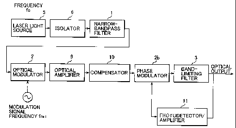
Figure 5 shows the arrangement of a first embodiment of the modulation
system of the present invention. This modulation system is provided with an
isolator 6 to suppress the effect of light returning back from the
narrow-bandpass filter 1, a dispersion compensator 10 for preventing the
efficiency of the reciprocating modulation from decreasing even at high-order
sideband frequencies, and an optical amplifier 9 for obtaining a high output.
The compensator 10 compensates for dispersion arising in the other components.
It is possible to dispense with the compensator 10 by equipping the other
system
components with this function.
The intensity of the optical output generally fluctuates. However, the
output can be kept stable by, for example, using a photodiode in a
photodetector/amplifier 11 to convert the optical output to an electrical
signal
that is fed back to the phase modulator 2b. This is because the fluctuations
in
the intensity of the optical output are caused by variations in the phase of
the
light arising from variations in the light path. Instead of the phase
modulator
2b, a modulator can be used that attenuates the carrier wave, leaving both
sidebands, such as the modulator described in "Optical Subcarrier Generation
CA 02342525 2001-07-06
-5-
Using Integrated LN Phase Modulator," by Shimozu, et al., C-3-20, 2000
General Meeting of The Institute of Electronics, Information and
Communication Engineers, p. 199. A semiconductor-based absorption
modulator, a Mach-Zehender interference type intensity modulator or an
electro-optic-effect phase modulator can be used for the modulator 2.
Modulation index can be readily improved by using resonance type
intensity and phase modulators that perform the modulation by using electrodes
that resonate at the modulation frequency. As can be readily understood, this
means that sufficient modulation can be obtained using just a small amount of
high-frequency power. The properties of a resonance type modulator are
described in "60 GHz Band Resonance Type LiNb03 Optical Modulator," by
Sasaki, et al., C-3-125, 2000 General Meeting of The Institute of Electronics,
Information and Communication Engineers, p. 279.
In the above-described modulator, as long as the optical amplifier 9 is
between the narrow-bandpass filter 1 and the band-limiting filter 3, the
precise
position has no particular significance. Similarly, there is no particular
significance attached to the order in which the modulator 2, optical amplifier
9,
compensator 10 and phase modulator 2b are arranged, because the same effect is
obtainable even if a different order is used.
As mentioned above, supplying another modulation signal to the phase
modulator 2b enables intensity-modulation of the optical output. As has also
been described above, while the intensity of the optical output generally
fluctuates, it can be kept stable by, for example, using a photodiode in the
photodetector/amplifier 11 to convert the optical output to an electrical
signal
that is used as feedback to the phase modulator.
Neat, an example of harmonic generation using the reciprocating optical
modulation system of the present invention will be described. Figure b is a
simplified representation of a second embodiment of the modulation system of
the invention. In Figure 6, light emitted by a laser light source 5 is
modulated
by a reciprocating optical modulator 4, which has optical filter properties,
producing double sidebands having frequencies equivalent to n times the
modulation frequency fm (where n is a predetermined positive integer 1, 3,
5...),
which are applied to a photodetector 12. The photodetector 12 is a nonlinear
element, and the result of this nonlinearity is an electrical signal having a
frequency that is n times the frequency differential of the two sidebands,
i.e. 2 x
fm.
Figure 7 shows a simplified representation of a third embodiment of the
modulation system of this invention. With respect to Figure 7, light from a
laser light source 5 is modulated by a reciprocating optical modulator 4,
which
has optical filter properties, producing a sideband having a frequency
equivalent
to n times the modulation frequency (where n is a predetermined positive
integer
1, 3, 5...). This sideband signal and light from the laser light source 5 are
CA 02342525 2001-07-06
-6-
applied to a photodetector 12. Owing to the nonlinear effect of the
photodetector 12, this gives rise to an electrical signal having a frequency
that is
the frequency differential between the sideband and the light from the laser
light
source 5. A filter 13 is used to select a signal of a predetermined frequency.
Again, it can readily be understood that there is no need to provide a light
path
to apply the light from the source 5 to the photodetector 12 in case there is
a
leakage of light from the source 5 that has passed through a modulator 4.
Below is described the effectiveness of the system of the present
invention having the configuration explained in the foregoing. The raodulation
system of the present invention comprises means that, taking n as a
predetermined integer of 1 or more, modulates light of a predetermined
frequency to produce a group of nth order sidebands thereof; means for
modulating the nth order sideband group to produce an (n+1)th order sideband
group; and means for selecting at least part of the (n+1)th order sideband
group.
By thus easing constraints with respect to electrical circuit performance,
this
makes it possible to obtain high-order sidebands in a planned way.
The system also includes a configuration in which reflection means are
used to fold the light path, making it possible to configure the system with a
short light path. The system also includes a configuration with a plurality of
modulation means, at least one of which receives the input of a group of
sidebands of different orders, which makes it possible to reduce the
manufacturing cost by decreasing the number of modulators used.
In another configuration, the modulation system includes first and
second reflection means, with the first reflection means transmitting
pre-modulation light of the predetermined frequency and reflecting light of
other
frequencies; and the second reflection means, with respect to the
predetermined
integer n of 1 or more, transmitting (n+1)th sidebands and reflecting other
light.
This enables a reciprocating optical modulation system to be readily
configured
using a filter that is transparent to a portion of the light to form an
optical
resonator.
The system can be configured with a laser light source, the first
reflection means comprising a narrow-bandpass filter, an optical modulator,
and
the second reflection mzans comprising a band-limiting filter, reducing the
cost.
Another arrangement in which the first reflection means comprises, a
narrow-bandpass filter, and the second reflection means comprises an optical
modulator, facilitates the modulation of optical signals.
The reciprocating optical modulation system also includes one having
means for converting part of the optical output into electrical signals, and
means
for re-applying the electrical signals to the modulation signal of the phase
modulator, which makes it possible to readily obtain a stable optical signal.
In
another arrangement that enables the system to multiply high-frequency
signals,
the system also includes means that uses a nonlinear element for combining a
CA 02342525 2001-07-06
portion of the tight input to the system with sideband signals output from the
system, and means for extracting electrical signals of a predetermined
frequency
band from the signals thus combined.