Note: Descriptions are shown in the official language in which they were submitted.
CA 02343261 2001-03-07
WO 00/14476 PCT/AU99/00733
1
MEASUREMENTS USING TUNNELLING CURRENT BETWEEN ELONGATE CONDUCTORS
Field of Invention
This invention relates to the accurate measurement and monitoring of fine
relative positions or displacements, eg. rotational or angular separations or
displacements, vibrations, linear separations or translations, alignments and
misalignments. Of particular, though not exclusive, interest is measurement of
angles.
Background Art
Known devices designed for ultra precise measurement of angles include
autocollimators, diffraction based systems and gears based systems.
Autocollimators use measurement of angular deviation to determine in turn, eg,
straightness, flatness, squareness and parallelism. Modern forms use laser
diode
light sources and beamsplitters, and incorporate a micrometer in the eyepiece
viewing system for accurate measurement of angular displacement. Typical best
accuracies are 0.2 arcseconds, for a measuring range of 160 arcseconds.
In a known goniometer-style instrument, a pair of radial gratings rotate in
unison at a uniform speed and are scanned by a pair of reading heads. One of
these is stationary while the other moves through the angle to be measured.
The
relative phase change between the two resultant signals is an indication of
the
rotation of the moveable reading head with respect to the fixed head. Accuracy
achieved is said to be 0.1 arcsecond.
These prior devices are relatively expensive and typically rather large
instruments. Often they form a key part of another scientific apparatus, such
as a
diffractemeter, where the precise measure of angle determines the resolution
and
quality of an instrument.
Accuracy of anguiar measurement is the subject of Zhang et al, "Improving
the Accuracy of Angle Measurement System with Optical Grating", Annals of the
_... ..~,......~....~.~_... _ ...._..~..,....,.,.,,.~m....
CA 02343261 2001-03-07
WO 00/14476 PCT/AU99/00733
2
CIRP Vol 43, No. 1 (1994). This paper proposes the use of index gratings with
sine function transmissivity, and other enhancements, and reports an accuracy
of
0.2 arcseconds with a prototype instrument.
It is an object of this invention to provide for fine measurement and
monitoring of relative positions or displacements, whether angular, linear or
otherwise, to a satisfactory accuracy that is preferably better than that
achieved
with known instruments and techniques.
Summary of the Invention
The invention proposes an approach quite different from that previously
used, and entails monitoring the quantum tunnelling current between two
proximate electrical conductors, preferably of nano dimensions. In a preferred
embodiment, two arrays of aligned conductors may be used, and these may
advantageously be carbon nanotubes.
The invention accordingly provides, in a first aspect, a method of measuring
and/or monitoring the relative position or displacement of two elements,
including:
associating the elements with respective elongate electrical conductors;
disposing the conductors preferably in approximate alignment, at a mutual
separation and applying an electrical potential difference such that there is
a detectable quantum tunnelling current between them; and
detecting and/or measuring said quantum tunnelling current.
Preferably, the relative positions of the conductors is adjusted to determine
that position at which maximum quantum tunnelling current is detected.
In a second aspect, the invention provides apparatus for use in measuring
and/or monitoring the relative position or displacement of two elements. The
apparatus includes a pair of elongate electrical conductors adapted to be
associated with the respective elements, and means for disposing the
conductors,
CA 02343261 2001-03-07
WO 00/14476 PCT/AU99/00733
3
preferably substantially aiigned in mutually parallel relationship, at a
mutual
separation such that a detectable quantum tunnelling current may be generated
between them on the application of an electrical potential difference between
the
conductors.
The apparatus may further include means to apply said potential difference,
and means to detect and/or measure the quantum tunnelling current between the
conductors.
Preferably, the apparatus further includes means to adjust the relative
positions of the conductors to determine that position at which maximum
quantum
tunnelling current is detected.
The position or displacement may be one or more of a rotational or angular
separation or displacement, a vibration, a linear separation or translation,
an
alignment and a misalignment.
Preferably, the electrical conductors are of width 1 micron or less eg, in one
or more embodiments, of width in the nano-order to sub-micron range. In the
latter
case, the conductors may be carbon nanotubes of arbitrary helicity or radius,
either single or multi-wails of carbon monofilaments, or nanowires.
Alternatively,
the conductors may be, eg, micron to sub-micron quasi one-dimensional
conductors. In some embodiments, the conductors may be of length 1 mm or less.
The conductors may be associated with the aforesaid elements by being
mounted in or on an insulating or semiconducting substrate, preferably flush
with a
surface of the substrate. The substrate may be, eg. a solid or a crystal face.
The
conductors may be placed along respective atomic steps on a vicinal surface.
Advantageously, the electrical conductors are arranged in respective
ordered grids or arrays of electrical conductor segments, preferably wired in
parallel e.g. through a single supply lead, which grids or arrays are
complementary
and overlaid to place the conductor segments in sufficient proximity to obtain
detectable quantum tunnelling currents.
CA 02343261 2001-03-07
WO 00/14476 PCT/AU99/00733
4
Brief Description of the Drawings
The invention will now be further described, by way of example only, with
respect to the accompanying drawings, in which:
Figure 1 is a fragmentary cross-section of a first embodiment of nano-
dimension device according to the invention, with the respective conductors
generally aligned and electrical connections diagrammatically depicted;
Figure 2 is a modification of the embodiment of Figure 1 in which the
conductors are substantially at right angles;
Figure 3 is a view similar to Figure 1 of an embodiment that utilises multiple
nanotube conductors;
Figure 4 is a view similar to Figure 2 of a modification of the embodiment of
Figure 3;
Figure 5 depicts a variation of the embodiment of Figure 3, formed in a
particular manner; and
Figure 6 is a view similar to Figures 1 and 3 of a further embodiment of the
invention that utilises an etched conductive overlay and a film applied by
Langmuir-Blodgett technology.
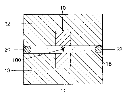
In the embodiment of Figure 1, respective nano-dimension elongate
electrically conductive wires 10, 11, of widths in the nano to sub-micron
dimension
range, are embedded flush in respective insulating medium substrates 12, 13.
In
this case, the wires are superposed in substantially aligned parallel
relationship, at
a separation or gap 18 in the range 2-50 Angstroms, such that when an
electrical
potential difference is applied by a potential source 26 across the
conductors,
there is a quantum tunnelling current 100 between them detectable in suitable
detection circuit 27.
w.. _.,_,~~.-,~.,.v._ ...__.,.~,..,__,.~...~........ . _._..._.~. _-__
CA 02343261 2001-03-07
WO 00/14476 PCT/AU99/00733
A suitable technique for making the embodiment is electron beam
nanolithography, in which aligned conducting wire can be delineated on a semi-
conducting substrate. This is described, eg. in Wilkinson et al, "Electron
Beam
Nanolithography", an article in the text "The Physics and Fabrication of
5 Microstructures and Microdevices" (eds. Kelly & Weisbuch, Spring-Verlag,
1986)
that describes and illustrates a set of parallel GaAs conducting wires on a
semi-
insulating substrate. In practical applications of the device, substrates or
plates 12,
13 are associated or coupled to respective elements whose displacement or
position is to be measured or monitored.
In general, tunnelling current 100 is proportional to the product of the local
densities of states on a pair of adjacent electrodes (ie. conductors), or in
other
terms, to the sum of the square of the tunnelling matrix elements between
states
on both electrodes. It is also a sensitive function of the tunnelling
potential and
the electrode curvature. Furthermore, quantum tunnelling current is critically
dependent on the spacing between the conductors because the quantum wave
function decays exponentially outside the conductor surface, and the detected
current will be a function of the relative angle between a pair of crossed
nanotubes. The invention takes advantage of the aforementioned exponential
and angular relationship in that the detected value of the tunnelling current
100 will
change sharply as the longitudinal opposed surface segments of the conductor
move apart with increasing rotational and/or translational misalignment or
vice
versa.
More particularly, suitable Schrodinger wave functions for the gap 18 are
found in Kiejna & Wojciechowski, "Metal Surface Electron Physics", Pergamon
(1996). It couid be demonstrated from wave function analysis that the quantum
tunnelling current is critically dependent on the spacing between the
conductors
because the quantum wave function decays exponentially outside the conductor
surface, and the detected current will also be a function of the relative
angle
between a pair of crossed nanoconductors.
The gap 18 between the aligned opposed conductor surface segments is
thought to be most appropriately in the range 2-50 Angstroms, more preferably
2-
CA 02343261 2001-03-07
WO 00/14476 PCT/AU99/00733
6
20 Angstroms. The conductor segments may conveniently be of any length that
can practicably be placed and aligned on the substrate and have leads
attached,
eg. in the range 1 p to 10-2m long.
Gap 18 may be a partial vacuum or may be filled with an appropriate
medium. Suitable arrangements for accurately maintaining the gap 18 include
the
use of buckyball (C60) nanobearings 20, 22, or the interpositioning of a
separation
film of an organic medium, preferably an organic lubricant eg. cyclohexane
(further
disclosed below). The latter is thought to be a particularly effective
approach to the
maintenance of accurately parallel fine separation.
The adjustment means may include piezoelectric positioners of known type
suitable for performing adjustments at nano dimension level.
The aforementioned effect is further enhanced if the conductors are
cylindrical, as for carbon nanotubes. In the case of the grids or arrays if
the
conductor segments are connected in parallel, there will be an amplifying
effect
and this will facilitate current measurement. However, if the lines have
independent connections, the grids forming the sandwich will be able to act as
two
dimensional arrays of point "capacitors" which can be switched on and off
independently, forming a "pixelised" array of tunnelling wells.
The tunnelling current 100 will exhibit minima at one or more positions
dependent on the aspect ratio (length to separation of conductor segments),
and a
maximum when the conductor segments of the two grids/arrays are perfectly
aligned.
Figure 3 illustrates an alternative embodiment in which the electrical
conductors comprise multiple parallel nanotubes 10a, 10b, 10c, 11 a, 11 b, 11
c
deposited on insulating medium substrates 12', 13'.
Procedures for producing a set of aligned nanotubes on a substrate are
described, for example, at Chauvet et al, Physical Review B52, 52 (1995); de
CA 02343261 2001-03-07
WO 00/14476 PCT/AU99/00733
7
Heer et al, Science 268, 845 (1995); and Kiang et al, Carbon 33, 903-914
(1995).
The properties of single wall nanotubes are described, for example, in
lijima, Nature 354, 56-58 (1991) and lijima et al, Nature 363, 603-605 (1993).
Carbon nanotubes of a variety of types are also described at Ostling et al,
Physical Review B. 55, 55 (1997).
A particular technique for producing a grid of parallel conductor segments
suitable for this invention is by epitaxial deposition of nanotubes or other
nano-
dimension conductors on the atomic steps of a vicinal surface produced by
slicing
a crystal at an angle to a primary plane. The separation of the conductor
segments may be regular or irregular, but is most preferably parallel. Figure
5
shows a modification of the embodiment of Figure 3 in which the nanotubes are
deposited in this way at the successive atomic steps 14, 15 on a stepped
vicinal
surface.
Figures 2 and 4 illustrate embodiments in which the respective arrays of
conductors of micron, submicron or nano-order dimensions when not nanotubes,
are arranged with the conductors 210 of one array in or on substrate 212,
extending substantially at right angles to the conductors 211 of the other
array, in
or on substrate 213. Instead of a right angle, the angular relationship may be
at
some other angle, eg. to form a diamond or rhomboidal type of two dimensional
lattice. In one application of such an arrangement preferabiy utilising a
large
number of conductor lines, the set of cross-over points 250 will form an
artificial
scattering lattice effective to scatter a beam of atoms directed parallel to
the
sandwich structure into the space 218 between the conductor arrays. If each
line
is independently electrically connected, ie they are not electrically in
parallel, there
will be a pixellised array which is an analog of a two-dimensional "pinball
game"
for atoms, with predefined scattering centres.
In a variation of the scattering lattice, it may further include an array of
magnetic elements forming the lattice and creating 1-dimensiona( domains at or
between the cross-over points.
_. _ _.....w...,.~:_M.:~. . ._
, r....~.,.,w.~,......_. . ~,.~m....e
CD/00370032.2 CA 02343261 2001-03-07 PCT/AU99/00733
Received 25 August 2000
-8-
Figure 6 is a further embodiment in which each substrate 312, 313 is
atomically smooth freshly cleaved mica, and the conductors 310, 311 are formed
by etching an overlay 330, 331 of gold, and then filling the interstitial
grooves by
application of a molecular monolayer by a Langmuir-Blodgett process. The two
arrays may be separated as before by a cyclohexane or other suitable organic
lubricant film 318 maintained by an outer thermoshrink wrap 340.
The illustrated devices are effective electro-mechanical nanodevices. On
the one hand, they may be applied to the measurement of angles, angles of
rotation, rotational speed, and alignment or misalignment at microscopic and
macroscopic level. Rotational speed can be measured, for example, by
measuring the number of current maxima per unit of time. It is thought to be
capable of an accuracy of the order of 0.01 arcseconds over an operational
angular range of 20 or so.
Alternatively, the illustrated devices may be used for measuring or
monitoring relative linear position or translation. If one substrate in the
embodiments of Figures 3, 5 and 6 is translated with respect to the other,
there
will be a series of very sharp peaks observed in tunnelling current 100. The
distance traversed will be given by the number of observed peaks times the
separation between the conductors; the resolution will be of the order of the
width
of the conductors, i.e. about 200 Angstroms with currently available
nanolithography technology, but about 10-30 Angstroms with nanotubes.
The rotational and translational effects would both contribute to vibration
monitoring or measurement, eg. in a seismograph.
,._