Note: Descriptions are shown in the official language in which they were submitted.
CA 02343409 2001-03-09
WO 00/17901 PCT/US99120099
MAGNETIC POLE INSENSITIVE SWITCH CIRCUIT
FIELD OF THE INVENTION
The present invention relates to switches and more particularly to switches
which are
responsive to magnet fields.
BACKGROUND OF THE INVENTION
As is known in the art, there exists a relatively large number of commercially
available
devices having a base or stationary portion and a movable cover or door
portion which include
a magnet. For example, telephones, cellular telephones, notebook or laptop
computers and
refrigerators include magnets in the moveable door or cover portions. The
covers are typically
opened and closed and, in some cases, the magnets provide a magnetic force
which maintains
the cover or door in a particular position {e.g. a closed position).
Such devices can also include detectors or sensors which indicate when a door
or cover
is in an open or a closed position. For example, cellular telephones (cell
phones) which are
provided as so-called "flip phones," include a base and a cover or "flip"
portion. The cover
has a magnet disposed therein. Disposed in the base portion of the cell phone
is a sensor.
When the cover is closed, the magnet is disposed over the sensor and the
sensor detects the
presence of the magnet's magnetic field. In response to the magnetic field,
the sensor provides
a signal which indicates that the cover is closed. Similarly, when the cover
is open, the
magnet (and hence the magnetic field) is removed from the sensor and the
sensor provides a
signal indicating that the cover is open.
In some applications, the sensor is provided as a Reed switch. The Reed switch
is a
mechanical type switch comprised of an evacuated glass tube having a series of
metal fingers
disposed therein. In response to the presence a magnetic field, the metal
fingers are in
mechanical contact thus providing a signal path having a short circuit
impedance characteristic
between the input and output terminals of the switch. Likewise, in the absence
of a magnetic
field, the mechanical fingers are not in contact thus providing a signal path
having an open
circuit impedance characteristic between the input and output terminals of the
switch.
CA 02343409 2006-10-30
7
Reed switches have the advantage that the switch operates regardless of the
orientation
of the magnet with respect to the switch. That is the Reed switch need not be
oriented in a
particular manner with respect to the poles of the magnet. This allows for
easy replacement
of the magnet or the Reed switch since there is no physical relationship
between them.
One probl~n with the Reed swjtch approach, however, is that the Reed switch is
relatively large and expensive when compared with semi-conductor type
switches. Also, the
Reed switch is a mechanical type switch and thus is not as reliable as a solid
state devices.
SUMMARY OF THE INVENTION
In view of the above problems with the prior art approach it has, in
accordance with
the present invention, been recognized that it would be desirable to provide a
replacement for
mechanical type switches such as Reed switches.
One problem with using a semiconductor switch in place of the Reed switch,
however
is that semiconductor devices, which include elements such as a Hall element,
must be aligned
in a particular manner with respect to the north and south poles of the
magnet. If the magnet
and Hall element are not properly oriented (i.e. the appropriate ends of the
hall element are
2 0 not aligned with the appropriate magnetic poles) then the semiconductor
switch will not operate
correctly. This leads to difficulties when it becomes necessary to replace the
magnet or the
semiconductor switch. For example, if a magnet must be replaced and neither
the magnet nor
the Hall element or switch are somehow coded so that it is known which end of
the magnet
to place at which end of the Hall element, then it is necessary to proceed by
trial and error to
2 5 determine how to install the replacement parts.
It would, therefore, be desirable to provide a reliable magnetic pole
insensitive switch
which can serve as a "drop-in" replacement for mechanical type switches such
as Reed
switches.
CA 02343409 2005-03-23
WO OOI17901 PCT/US99IZ0099
3
It would also be desirable to use a semiconductor switch including a Hall
effect element
as a drop in replacement for a Reed switch type device, however this requires
the Hall element
to be insensitive as to whether a north pole or south pole is being sensed.
In accordance with the present invention, a sensor for sensing an article
which provides
a magnetic field it~sludes a magnetic-field-to-voltage transducer for
generating at an output
thereof a first signal voltage having a signal voltage level which is
proportional to a magnetic
field having a first polarity and a second signal voltage having a signal
voltage level that is
proportional to a magnetic field having a second different polarity and a
window comparator
having an input port coupled to the output port of the magnetic-field-to-
voltage transducer to
receive the first and second signa! voltages and to provide an output signal
having a first value
when the article is within a first predetermined distance of the magnetic-
field-to-voltage
transducer regardless of the polarity of the magnetic field. With this
particular arrangement,
a drop in replacement for a Reed switch type device which is insensitive as to
whether a north
pole or south pole is being sensed is provided. By providing the comparator as
a window or
symmetrical comparator (i.e., a comparator having the same switching point for
positive and
negative magnetic fields) the sensor operates correctly regardless of the
orientation of the
magnet relative to the magnetic-field-to-voltage transducer.
In accordance with a further aspect of the present invention, a switch
includes a Hall
element and a threshold detector circuit having a substantially similar
switching point for
positive and negative magnetic fields. With this particular arrangement, a
switch which
utilizes a Hall effect device can operate correctly regardless of the
orientation of the magnetic
poles with respect to the Hall device. In one embodiment, the threshold
circuit is provided as
2 5 a comparator circuit.
CA 02343409 2005-10-26
3a
In accordance with a further aspect, the present invention seeks to provide a
circuit
comprising:
a sensor having at least one output port at which a first signal voltage is
provided in
response to a presence of a magnetic field of a first polarity and at which a
second signal
voltage is provided in response to a presence of magnetic field of a second
polarity; and
a detector having at least one input port coupled to the at least one output
port of the
sensor and an output port at which an output signal is provided, the output
signal being
indicative of the presence of said magnetic field of said first polarity and
the presence of said
magnetic field of said second polarity, said detector comprising a first
circuit for comparing
said first signal voltage to a first threshold level and a second circuit for
comparing said
second signal voltage to a second threshold level, wherein said first and
second threshold
levels are adjustable with a common adjustment mechanism.
In accordance with a further aspect, the present invention seeks to provide in
a
wireless communication device, a switching system for providing a signal in
response to an
article which provides a magnetic field, the switching system comprising:
(a) a sensor for sensing the magnetic field of the magnetic article, said
sensor for
generating a first signal voltage having a signal voltage level which is
proportional to a
magnetic field having a first polarity and a second signal voltage having a
signal voltage level
that is proportional to a magnetic field having a second different polarity;
and
(b) a threshold detection circuit coupled to the sensor to receive the first
and second
signal voltages and responsive to a supply voltage to provide an output signal
having a first
value when said magnetic article is within a predetermined distance of the
sensor regardless
of the polarity of the magnetic field, said threshold detection circuit
comprising a first circuit
for comparing said first signal voltage to a first threshold level and a
second circuit for
comparing said second signal voltage to a second threshold level, wherein said
first and
second threshold levels are substantially constant in response to variations
in said supply
voltage.
CA 02343409 2005-10-26
3b
In accordance with a further aspect, the present invention seeks to provide a
switching
system for providing a signal in response to a magnetic article which provides
a magnetic
field, the switching system comprising:
(a) a sensor for sensing the magnetic field of the magnetic article, said
sensor for
generating a first signal voltage having a signal voltage level which is
proportional to a
magnetic field having a first polarity and a second signal voltage having a
signal voltage level
that is proportional to a magnetic field having a second different polarity,
wherein said sensor
is a Hall element circuit;
(b) a threshold detection circuit coupled to the Hall element circuit to
receive the first
and second signal voltages and responsive to a supply voltage to provide an
output signal
having a first value when said magnetic article is within a predetermined
distance of the
sensor regardless of the polarity of the magnetic field with respect to said
Hall element circuit,
said threshold detection circuit comprising a first circuit for comparing said
first signal
voltage to a first threshold level and a second circuit for comparing said
second signal voltage
to a second threshold level, wherein said first and second threshold levels
are substantially
constant in response to variations in said supply voltage, wherein said
threshold detection
circuit is a window comparator comprising first and second differential pair
circuits, each
having an input terminal coupled to one of a pair of outputs from said Hall
element circuit and
an output terminal coupled to an output terminal of said comparator; and
(c) a filter and level shifter circuit coupled between said Hall element
circuit and said
comparator.
In accordance with a further aspect, the present invention seeks to provide a
switching
system for providing a signal in response to a magnetic article which provides
a magnetic
field, the switching system comprising:
(a) a sensor for sensing the magnetic field of the magnetic article, said
sensor for
generating a first signal voltage having a signal voltage level which is
proportional to a
magnetic field having a first polarity and a second signal voltage having a
signal voltage level
CA 02343409 2005-10-26
3c
that is proportional to a magnetic field having a second different polarity,
wherein said sensor
is a Hall element circuit;
(b) a threshold detection circuit coupled to the Hall element circuit to
receive the first
and second signal voltages and responsive to a supply voltage to provide an
output signal
having a first value when said magnetic article is within a predetermined
distance of the
sensor regardless of the polarity of the magnetic field with respect to said
Hall element circuit,
said threshold detection circuit comprising a first circuit for comparing said
first signal
voltage to a first threshold level and a second circuit for comparing said
second signal voltage
to a second threshold level, wherein said first and second threshold levels
are substantially
constant in response to variations in said supply voltage, wherein said
threshold detection
circuit is a window comparator comprising it and second differential pair
circuits, each having
an input terminal coupled to one of a pair of outputs from said Hall element
circuit and an
output terminal coupled to an output terminal of said comparator;
(c) first and second output amplifier stages, each of the output amplifier
stages
coupled between a respective one of the output terminals of the first and
second differential
pair circuits and the output terminal of said comparator; and
(d) an output/buffer amplifier stage having an input terminal coupled to the
output
terminal of each of said first and second output amplifier stages and having
an output terminal
coupled to the output terminal of said comparator.
In accordance with a further aspect, the present invention seeks to provide a
switching
system for providing a signal in response to an article which provides a
magnetic field, the
switching system comprising:
(a) a sensor for sensing the magnetic field of the magnetic article, said
sensor for
generating a first signal voltage having a signal voltage level which is
proportional to a
magnetic field having a first polarity and a second signal voltage having a
signal voltage level
that is proportional to a magnetic field having a second different polarity;
and
(b) a threshold detection circuit coupled to the sensor to receive the first
and second
signal voltages and responsive to a supply voltage to provide an output signal
having a first
CA 02343409 2005-10-26
3d
value when said magnetic article is within a predetermined distance of the
sensor regardless
of the polarity of the magnetic field, said threshold detection circuit
comprising a first circuit
for comparing said first signal voltage to a first threshold level and a
second circuit for
comparing said second signal voltage to a second threshold level, wherein said
first and
second threshold levels are substantially constant in response to variations
in said supply
voltage.
In accordance with a further aspect, the present invention seeks to provide a
cellular
telephone comprising:
a base;
a cover having a first end movably coupled to said base and a second end;
a magnetic article disposed in the second end of said cover, said magnetic
article
having a first pole and a second pole; and
a switch disposed in said base, said switch comprising:
a sensor for sensing the magnetic field of the magnetic article, said sensor
for
generating a first signal voltage having a signal voltage level which is
proportional to a
magnetic field having a first polarity and a second opposite signal voltage
having an opposite
signal voltage level that is proportional to a magnetic field having a second
different polarity;
and
a comparator coupled to the sensor to receive the first and second signal
voltages and
to provide an output signal having a first value when said magnetic article is
within a
predetermined distance of the sensor regardless of the polarity of the
magnetic field.
In accordance with a further aspect, the present invention seeks to provide a
method of
switching in a wireless communication device comprising the steps of
(a) sensing with a magnetic field sensing element a magnetic field provided by
a
magnetic article having a first pole region and a second pole region wherein
said magnetic
CA 02343409 2005-10-26
3e
article has first magnetic field polarity at the first pole region and a
second different magnetic
field polarity at the second pole region;
(b) generating a sensor output signal having a signal level which is
proportional to the
magnetic field sensed in step (a), wherein the sensor output signal has a
first signal direction
when said first pole region is proximate said magnetic field sensing element
and a second
opposite signal direction when said second pole region is proximate said
magnetic field
sensing element;
(c) comprising the sensor output signal to one of first and second threshold
signal
levels; and
(d) in response to the sensor output signal level reaching or exceeding the
one of the
first and second threshold signal levels, providing an output signal having a
first signal level
regardless of the direction of the sensor output signal.
In accordance with a further aspect, the present invention seeks to provide a
method of
switching comprising the steps of
(a) sensing with a magnetic field sensing element a magnetic field provided by
a
magnetic article having a first pole region on a first substantially flat
surface and a second
pole region on said first surface wherein said magnetic article has first
magnetic field polarity
at the first pole region and a second different magnetic field polarity at the
second pole
region;
(b) generating a sensor output signal having a signal level which is
proportional to the
magnetic field sensed in step (a), wherein the sensor output signal has a
first signal direction
when the first pole region is proximate said magnetic field sensing element
and a second
opposite signal direction when the second pole region is proximate said
magnetic field
sensing element;
(c) comparing the sensor output signal to at least one of first and second
threshold
signal levels; and
(d) in response to the sensor output signal level reaching or exceeding the
one of the
first and second threshold signal levels, providing an output signal having
the same signal
CA 02343409 2005-10-26
3f
level when the sensor output signal has the first signal direction as when the
sensor output
signal has the opposite signal direction.
In accordance with a further aspect, the present invention seeks to provide a
device
comprising any device or apparatus which uses a magnetic device in conjunction
with a
movable portion:
a base;
an element movably coupled to said base;
a magnetic article disposed in a selected one of said base and said element;
and
a switch disposed in the other one of said base and said element, said switch
comprising:
a sensor for sensing the magnetic field of the magnetic article and for
generating a first
signal having a signal level proportional to a magnetic field of a first
polarity and a second
signal having an opposite signal level proportional to a magnetic field of a
second different
polarity; and
a comparator coupled to the sensor to receive the first and second signals and
to
provide an output signal having the same value when said magnetic article is
within a
predetermined distance of the sensor and the magnetic field of the magnetic
article has the
first polarity as when the magnetic article is within a predetermined distance
of the sensor and
the magnetic field of the magnetic article has the second different polarity.
BRIEF DESCRIPTION OF THE DRAWINGS
The foregoing features of this invention as well as the invention itself may
be more
fully understood from the following detailed description of the drawings in
which:
CA 02343409 2001-03-09
WO 00/17901 PCT/US99/20099
4
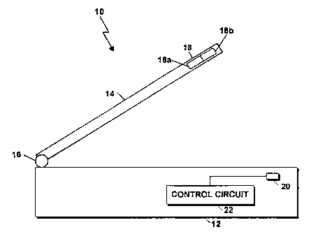
FIG. I is a block diagram of a cellular telephone including a magnetic pole
insensitive
switch in accordance with the present invention;
FIG. 2 is a block diagram of a magnetic pole insensitive switch;
FIG. 3 is a schematic diagram of a comparator;
FIG. 3A is a plot of window comparator input voltage versus output voltage;
FIG. 4 is.'-a"schematic diagram of a switch circuit utilizing a comparator;
FIG. 4A is a plot of voltage versus magnetic field; and
FIG. S is a schematic diagram of a switch circuit including a magnetic-field-
to-voltage
transducer.
DETAILED DESCRIPTION OF THE INVENTION
The following description sets forth an exemplary embodiment in which the
present
invention may be used. Specifically, certain reference is made below to a
cellular telephone
(cell phone) application. It should be understood, however, that the present
invention finds
use in a wide variety of applications and devices and is not limited to the
exemplary
embodiment described below. For example, the invention may be used in any
device or
apparatus which uses a magnetic device in conjunction with a movable portion
such as a
movable cover or door including cellular and non-cellular telephones, notebook
or laptop
computers and refrigerators.
Referring now to FIG. 1, a cellular telephone (cell phone) 10 includes a base
portion
12 having a first end of a cover 14 movably coupled thereto. In this
particular example, the
first end of the cover 14 is movably coupled to the base 12 through a
rotatable joint 16. Those
of ordinary skill in the art will recognize of course that any coupling device
or means which
2 5 allows the cover 14 to move with respect to base 12 maybe used in place of
rotatable joint 16.
Disposed in the second end of the cover 14 is a magnetic article 18 such as a
magnet.
The magnet 18 has a first pole 18a and a second pole 18b. Depending upon how
the magnet
18 is disposed in the cover 14 the first pole 18a may correspond to a north or
south pole of the
magnet and the second pole 18b will correspond to the other pole of the
magnet.
CA 02343409 2001-03-09
WO 00/17901 PCT/US99/20099
Disposed in the base 12 is a semiconductor switch 20 which operates regardless
of the
orientation of the magnetic poles of magnet 18. One possible embodiment of the
switch is
described in detail below in conjunction with FIGS. 2-5. Suffice it here to
say that switch 20
5 includes a sensor for sensing the magnetic field of the magnet 18 and a
threshold detection
circuit or compafa~,or.
The transducer provides a transducer output signal having a signal level which
varies
depending upon the orientation of the magnet 18 to the sensor. Thus, the
transducer generates
a first signal voltage having a signal voltage level which is proportional to
a magnetic field
having a first polarity and a second opposite signal voltage having an
opposite signal voltage
level that is proportional to a magnetic field having a second different
polarity. In one
embodiment, the transducer may be provided as a magnetic-field-to-voltage
transducer.
Switch 20 also includes a comparator coupled to the transducer to receive the
first and
second signal voltages and to provide an output signal having a first value
when the article is
within a first predetermined distance of the magnetic-field-to-voltage
transducer regardless of
the polarity of the magnetic field. Thus, when the cover 14 is open the magnet
18 is displaced
from the switch 20 and the switch 20 provides a switch signal having a first
predetermined
signal level regardless of the orientation of the magnet 18 with respect to
the switch 20.
Similarly, when the cover 14 is closed the magnet is proximate the switch 20
and the switch
20 provides a switch signal having a second predetermined signal level
regardless of the
orientation of the magnet 18 with respect to the switch 20.
2 5 The signal provided by switch 20 merely indicates whether the cover 14 is
open or
closed. Thus, when the cover is closed, the switch provides a first signal
having a first value
and when the cover 14 is open, the switch 20 provides a second signal having a
second
different value.
CA 02343409 2001-03-09
WO 00/17901 PCT/US99/20099
6
The signals provided by the switch 20 are coupled to a control circuit 22. The
control
circuit 22 implements, or causes to be implemented, certain functions
depending upon the
position of the cover 14 (i.e. depending upon whether the cover 14 is open or
closed). For,
example, when the cover is closed, switch 20 provides a signal to control
circuit 22 so
indicating and control circuit 22 may cause cell phone 10 to operate in a
power saver mode.
''';
Referring now to FIG. 2, the switch 20 is shown to include a Hall effect
device 30
coupled to a comparator 32. In accordance with the present invention, the Hall
effect device
30 functions with the comparator 32 to provide proper operation regardless of
the orientation
of the magnet 18 with respect to the Hall effect device 30.
The Hall effect device 30 acts as a magnetic-field-to-voltage transducer which
generates
at output terminals 31a, 31b a first signal voltage having a first signal
level voltage which is
proportional to a magnetic field having a first polarity and a second signal
voltage having a
second signal voltage level that is proportional to a magnetic field having a
second different
polarity. The comparator 32 receives the signals on terminals 31a, 31b.
It will be appreciated by those of ordinary skill in the art that other
magnetic-field-to-
voltage transducers may be used. As one example, the Hall effect device 30 may
be replaced
with a magneto-resistive bridge, including a magneto-resistive element and a
bridge
configuration, such as a Wheatstone bridge. The magneto-resistive element is a
resistive
device, such as a metallic thin film resistor, having a resistance that
changes depending on the
angle between the flux and the device. More particularly, the magneto-
resistive element senses
flux parallel to the plane of the device and normal to current flow.
The comparator 32 provides an output signal having a first value when the
magnet 18
is within a first predetermined distance of the transducer 30 regardless of
the polarity of the
magnet 18. The comparator 32 provides an output signal having a second
different value when
the magnet 18 is not within the first predetermined distance of the transducer
30 regardless of
3 0 the polarity of the magnet 18. Thus, regardless of whether the second end
18b of magnet 18
CA 02343409 2001-03-09
WO 00/17901 PCT/US99/20099
7
is a north or a south pole, the switch 20 provides a signal indicating whether
the magnet 18
is proximate the sensor 14. Thus, the switch 20 provides, for example, an
indication of
whether the cover 14 (FIG. 1) is opened or closed.
Referring now to FIG. 3, a comparator circuit 35 has a plurality of terminals,
35a-35e,
and includes first~d second and comparators 36, 38. The comparator 36 has a
first terminal
36a coupled to a first reference voltage V.,." at terminal 35a, a second input
terminal 36b
coupled to an input voltage V,N at terminal 35b and an output terminal 36c
coupled to
comparator circuit output terminal 35d where an output voltage Vo~,~ is
provided. A reference
voltage, V,~F is coupled to terminal 35e and provides a reference voltage to
comparators 36,
38.
The comparator 38 includes a first input terminal 38a coupled at input port
35b to the
input voltage V,N and a second input terminal, 38b, coupled to a threshold
voltage V.,.,, at
terminal 35c. An output terminal 38c of comparator 38 is coupled to provide
the output
voltage V~UT at the output terminal 35d.
In this particular embodiment, comparators 36, 38 are provided having a means
for
including hysteresis such that the reference or threshold voltages V.,.,,,
V.,.,, can be represented
2 0 as V.,H+ and V.".,_ and V.,.,,+ and V.,.,r, respectively. The values
V.".,+, V.,.E,_, Vz.~+, VTU represent
the comparator switch points depending upon the value of the output voltage
Vo~rT. As
indicated in FIG. 3A, once the output voltage V~",.,. switches (e.g. from a
high level to a low
level), then the switch point changes from V.,.~+ to V.,.f,_. Likewise, once
the output voltage
VouT switches from a low level to a high level, then the switch point changes
from V.,H_ to
2 5 V.,.,,+
As can be seen in FIG. 3A, the same holds true as the input voltage V,N
assumes
negative voltages (i.e. voltage values on the left hand side of the Y-axis in
FIG. 3A). That
is, once the output voltage VoU,. switches then the switch point changes from -
V.,.~+ to -V.,~, and
CA 02343409 2001-03-09
WO 00/17901 PCT/US99/20099
8
vice-versa depending upon whether the output is switching from low to high or
from high to
low.
If the output voltage V~IIT is high and the input voltage V,N has a value
greater than or
equal to zero, when the input voltage V,N meets or exceeds the voltage V.,~,+,
the output
voltage switches ~f~c~n a value of VHICH to Vu,W and the switch point changes
from V.~.,+ to V.".,.
. Thus the value of the output voltage Vo~,.,. will not switch from VFW to
VHroH until the input
voltage V,N reaches the value V.,.,.,_.
It should be appreciated that in other embodiments and applications it may be
preferable to utilize comparators which do not have hysteresis and thus
switching occurs at a
single voltage level, namely V.,.,.,.
In operation, and with reference now to FIG. 3A, the input voltage V,N is
generated
in response to a magnetic field being provided to and removed from a magnetic
field sensing
device which senses the magnetic field and provides a corresponding signal in
response
thereto. As discussed above in conjunction with FIG. 1, such a magnetic field
could be
provided from the opening and closing of a cover having a magnetic article
provided therein.
2 0 If the magnetic field sensing circuit is provided as a Hall device, a
signal voltage is
provided. Assuming the input voltage V,N is at or near zero volts (i.e. V,~ =
0 volts), the
output voltage VoUT is at a first predetermined voltage level V,~~;H which may
correspond for
example to a so-called transistor-transistor-logic (TTL) high voltage level.
In response to a
magnetic field, the HaII device provides either a positive or a negative input
voltage V,N. If
the input voltage provided by the Hall device moves in a positive direction
from zero volts
toward the threshold voltage, V.,.,.,+, when the threshold voltage meets
and/or exceeds the
threshold voltage level V.,.E,+, then the output voltage V~,~,T changes from
the predetermined
signal level, VH,cH to a second predetermined voltage level Vu,W which may
correspond for
example to a so-called TTL low voltage level. When the input voltage moves
past the
CA 02343409 2001-03-09
WO 00/17901 PCT/US99/20099
9
threshold voltage V.,.H_ in a negative-going direction, the output voltage
changes from V,pW
back to V,~,GH.
Likewise, as the input voltage moves in a negative direction from zero volts
and
reaches and/or exceeds the threshold voltage -V~.,.+, the output voltage VoLrr
changes from the
first value VH,cH'tpa,the second value V,~W. Similarly, as the input voltage
V,N moves from -
V.,.,.+ and reaches and/or exceeds the voltage level -V~.r,_, the voltage
level then changes from
the output voltage level V,pW to V",cH .
Referring now to FIGs. 4 and 4A, a switching circuit 40 includes a sensing and
control
circuit 44 which includes a magnetic field detection circuit 46 coupled to a
comparator circuit
4$. Comparator circuit 48 can include the necessary circuitry (e.g. bias
circuits) to provide
an appropriate control signal to the control terminal of a switch 50 in
response to signals
provided from the magnetic field detection circuit 46. In one embodiment, the
magnetic field
detection circuit may include a Hall element which provides an output voltage
signal in
response to the presence or absence of a magnetic field. In this particular
embodiment, the
output of comparator 48 is fed to the switch through an optional inverter
circuit 51. Inverter
circuit 51 is here included to maintain the consistency between the logic
implemented by the
circuit of FIG. 4 and the logic implemented by the circuits of FIGs. 3 and 5
in an effort to
2 0 simplify the corresponding descriptions of each of the figures.
The sensing and control circuit 44 provides a comparator output signal at
terminal 44a
to a control terminal SOa of a switch circuit 50. In this embodiment, the
switch circuit 50 is
shown as a transistor switch and in particular is shown as a bi-polar junction
transistor (BJT).
2 5 In this case, the control terminal SOa corresponds to a base terminal of
the transistor 50. A
second terminal SOb of the transistor SO is coupled through a resistor 52 to a
power supply 54
and to an output terminal 40a. A third transistor terminal SOc is coupled to a
first reference
potential, here corresponding to ground. It should be noted that although the
switch circuit
50 is here shown as a BJT, those of ordinary skill in the art will appreciate
that other types of
CA 02343409 2001-03-09
WO 00/17901 PCT/US99/20099
transistors may also be used. For example, in some embodiments, it may be
preferable to use
a field effect transistor (FET).
Depending upon the proximity of a magnetic article to the magnetic detection
circuit,
5 the output signal provided at the output terminal 40a has one of a first and
a second voltage
level. When the'~agnetic field detection circuit 46 senses a strong magnetic
field (such as
would be the case, for example, with the cover 14 in FIG. 1 in the closed
position), the
comparator 48 provides a first or high signal voltage at control terminal 50a
and thus biases
the switch circuit 50 into its conductive state. In its conductive state, the
switch transistor 50
10 provides a signal path having a relatively low impedance characteristic
between the transistor
terminals SOb and SOc and thus causes the output voltage V~~,T at the output
terminal 40a to
be a low voltage.
Similarly, with the cover open, magnetic field detection circuit 46 senses a
relatively
weak magnetic field and the comparator 48 provides a low signal voltage at the
control
terminal SOa and thus biases transistor SO into its non-conductive state. In
its non-conductive
state, the transistor 50 provides a signal path having a relatively high
impedance characteristic
between the transistor terminals 50b and SOc and thus causes the output
voltage Vo~,.,. at output
terminal 40a to be a high voltage.
Refernng briefly to FIG. 4A, the output voltage Vo~,T vs. the magnetic field
strength
B is shown. As can be seen from the plot of FIG. 4A, when the strength of the
magnetic field
B reaches an operating point level, Bo,, the output voltage V~~,T maintains a
low signal level
and when the magnetic field level reaches a release point level, B~, the
output voltage VouT
2 5 reaches a high signal level. It should thus be nated that the sensing and
control circuit 42 in
combination with transistor 50 provide the appropriate signal levels
regardless of whether the
magnetic field is a positive field or a negative field (i.e., a north or a
south pole). Thus, as
shown in Tables I and II below, the switching circuit 40 provides the correct
signal to the
control circuit 22 (FIG. 1).
CA 02343409 2001-03-09
WO 00/17901 PCTNS99/20099
TABLE I
COVER COMPARATOR TRANSISTOR
POSITION OUTPUT STATE VouT
CLOSED LOW ON LOW
OPEN HIGH OFF HIGH
Table I shows that when a magnetic field is detected, the comparator 48
provides a
signal which biases the transistor 50 into its conductive state (i.e. the
transistor is ON). This
results in the signal level of the signal V~~,T being low. Similarly, when no
magnetic field is
detected, the comparator 48 provides a signal which biases the transistor 50
into its non-
conductive state (i.e. the transistor is OFF). This results in the signal
level of the signal Vo~,T
being high. It should be noted that column of Table I labeled "Comparator
Output" refers to
the output of the comparator 48 prior to the inverter circuit.
Referring now to FIG. 5, a switch circuit 58 includes a magnetic-field-to-
voltage
transducer provided from a Hall element circuit 60 and a comparator 62. In
this particular
embodiment, the Hall element circuit 60 has a pair of outputs connected
differentially to a pair
of input terminals 62a, 62b of a window comparator 62.
The Hall element 60 is mounted such that the Hall voltage increases or
decreases based
2 0 upon the proximity of a magnet (not shown) to the Hall element 60.
Alternatively, the
detector circuit of FIG. 4 may be used to detect articles that themselves are
magnetized.
The Hall voltage signal is manipulated by the window comparator circuitry 62
to
produce an output signal VouT which provides an indication of whether any
magnetic particle
is within a predetermined distance of the Hall element 60.
CA 02343409 2006-10-30
12
The differential input signal is coupled- through a filter and level shifter
circuit 64. It
should be appreciated that in an alternative embodiment the filter and level
shifter circuit 64
could be provided as part of the Hall element circuit 60 rather than as part
of the comparator
circuit 62. The appropriately filtered and level shifted signals are coupled
from the filter and
level shifter circuit 64 to respective ones of differential pair circuits 66a,
66b.
Each of the differential pair circuits 66a or 66b, are provided to accept
signals
generated by the interaction of Hall circuit 6(? with a respective one of the
north or south poles
of a magnet. As shown in Table II, the relationship of the magnet polarity to
the Hall effect
device (i.e. the orientation of the north and south magnet poles with respect
to the Hall device)
determines the output values provided by each the two differential pair
circuits.
The output signals provided by the differential pair circuits 66a, 66b are fed
to
respective ones of output amplifier stages 68a, 68b. The output amplifier
stages 68 convert the differential voltage provided from differential pair
circuits 66a, 66b into
a single ended voltage which drives the inverter the inverter circuit 70.
Those of ordinary skill
in the art appreciate, however, that inverter circuits can be driven with
single or differential
lines. Those of ordinary skill in the art will also appreciate when it is
preferable to drive an
inverter circuit with differential lines rather than a single Iine.
The signals are then fed to an output/buffer amplifier stage 70 which is
coupled to the
output port 62c of the comparator 62. Comparator circuit 62 also includes a
circuit 76 which
includes a plurality of current sources which provide control signals to
differential pair circuits
66a, 66b and to buffer circuit 68a, 68b.
A temperature and voltage compensation circuit 80 includes a plurality of
current sinks
72a - 72c which allow the comparator 62 to operate properly while withstanding
a relatively
wide range of voltage and temperature changes.
CA 02343409 2001-03-09
WO 00/17901 PCT/US99/20099
13
This is particularly important in devices, such as cell phones for example, in
which the
normal operating voltage of the device is relatively low (to conserve battery
power and to
operate in a power conservation mode, for example). Such low normal operating
voltages
combined with varying temperature ranges and variations due to standard
manufacturing
processes used to fabricate circuits, makes it relatively difficult to
maintain switch points of
comparator 62. ~'f'~overcome difficulties, a comparator bias circuit 80 allows
the comparator
62 to withstand low voltages which change by plus and minus 20%. To maintain
the switch
points of comparator 62 fixed over this relatively wide range of voltages, the
comparator bias
circuit 80 provides compensation signals to comparator 62 to allow the
comparator 62 to
operate over a wide range of voltage, temperature and process variations.
The dash line 81 between the current source 72c and the output terminal 62c
indicates
that the output controls the current source 72c. A first output level causes
current source 72c
to produce a relatively low current and a second different output level causes
signal source 72c
to produce a relatively high current.
As discussed above in conjunction with FIGs. 3 and 3A and as implemented in
the
circuit of FIG. 5, if an input voltage from the Hall circuit 60 is equal to
zero volts and is
increasing in a positive direction, then the output voltage V~~,T switches
once the voltage level
2 0 reaches and/or exceeds the threshold voltage V.",+ thereby causing the
output voltage V~LrT to
go low (i.e. assume a voltage level of V,~W). Depending upon whether the
output voltage
Vow is high or low, a differential voltage drop exists across one of the
resistors R3 or R4
which are coupled to source 72c. Thus, controlling the current source 72c
changes the value
which causes the differential voltage drop across either resistor R3 or R4 and
causes the switch
point to be changed from V.rH+ to V.,.f,_ or vice-versa (and similarly causes
the switch points to
be changed from -V.,.,_,+ to -V.L~,_~.
Table II below shows the output signal value V~,~r,. and the operation of the
differential
pair comparator circuits 66a, 66b with respect to the magnetic field
characteristics.
CA 02343409 2001-03-09
WO 00/17901 PCTNS99/20099
l4
TABLE II
MAGNETIC FIELD DIFF. DIFF. COMP.
PAIR ~/ PAIR OUTPUT VouT
1 #2
RELATIVE V,N POLARITY
STRENGTH
STRONG SOUTH POSITIVE ON OFF LOW LOW
WEAK SOUTH POSITIVE OFF OFF HIGH HIGH
WEAK NORTH NEGATIVE OFF OFF HIGH HIGH
STRONG NORTH NEGATIVE OFF ON LOW LOW
As noted above the comparator 62 is symmetrical and thus (as illustrated in
FIG.
3A) there is the same switching point for positive and negative magnetic
fields.
The symmetrical comparator 62 of the present invention provides several
advantages
including: similar operation for both polarities of a magnet and operation
which is
independent of power supply voltage.
The comparator 62 and the bias circuit 80 may be implemented as a single
integrated circuit to thus provide a relatively compact semiconductor switch
circuit which is
magnetic pole insensitive.
Having described preferred embodiments of the invention, one of ordinary skill
in
the art will now realize further features and advantages of the invention from
the above-
described embodiments. It should be understood, therefore, that the foregoing
is only
2 0 illustrative of the principles of the invention and that various
modifications can be made by
those skilled in the art without departing from the scope and spirit of the
invention.
CA 02343409 2005-03-23
wo oon~9o~ ~crius~noo9Q
Accordingly, the invention is not to be limited by what has been particularly
shown and
described, except as indicated by the appended claims.