Note: Descriptions are shown in the official language in which they were submitted.
CA 02343780 2001-03-12
:~~:=i'i.ii:J::='!.': ~~Q\4\:r:>.iii::i\K,
. :=. .'::: ~:~~=:l .=.,. ' i}i};:A:'},.4.i..i:.: i' i:iji:i.
':~:?!1,'.4:::~:~~::
;;~i'~õ~,:,,~,.=,.,,.,.,..,'.,.~~'.,.,.,+,,.,~,.',,.v.~,.,,='.=. ?:'vi =..:v
..: .... .............. . . . .. '::~2.
......................... . ... . ..n........................
..................:C'~~.~
OPTICAL PHASE DETECTOR
The invention relates to an optical phase detector for measuring the phase
difference between two input signals. The invention also relates to
applications
of an optical phase detector, including use in an optical frequency
discriminator
and a laser stabilisation apparatus.
By way of background to the present invention, US5396166 describes a fibre
optic interferometer sensor system including a fibre optic interferometer
having
an electrostrictive transducer bonded to one of the first and second optical
fibre
arms of the interferometer. The electrostrictive transducer has non-linear
characteristics which enables detection of low frequency or DC signals at side
bands of a high frequency carrier. Also by way of background to the invention,
EP0388929 describes a fibre optic laser gyro in which a modulated phase
difference is detected between two rays of light phase modulated by means of a
phase modulator having propagated through an optical fibre coil in opposite
directions and having interfered with each other.
Conventionally, phase difference may be measured optically by interfering two
beams to form an interference fringe pattern and measuring the fringe pattern
as
it moves across a camera face due to a change in the relative phase. A
disadvantage of this type of measurement is that it relies on the counting of
fringes and interpolation between fringes to measure phase or position
accurately. This process can be relatively slow and not especially accurate.
Such detectors may be used in displacement measurement schemes, such as in
laser metrology, to measure position accurately i.e. to a fraction of an
optical
wavelength.
:::F?':'ri~'t~D>
CA 02343780 2001-03-12
_ ,..:::;;, =.,;.:x=:. .
~...... ~. ..
.~=. '~=,'s~3
.,ti .
%:~:~it?=:'='~~~~~ :::~~=:.: ~ .,.. .-..,.. . ..:. ,. =.
; . r..
'=..:~':..; .:~:
.. .... . ...~~~~:;:~:: ~~~Y~~1..;',;='=:;:~..,= ,
, ................._....._ :.:..... ,..._...............:;;c.:.:::\~
.2-
Optical techniques have previously been used for the generation of microwave
radiation, by mixing two stable lasers, and for phased array antenna beam-
forming, in which simple optical systems are used to perform a complicated
microwave function. A known technique for the generation of stabilised
microwave radiation has been achieved by incorporating a fibre optic delay
line
in an RF, microwave or millimetre wave (mm-wave) frequency discriminator
circuit. This enables the difference in frequency of two stable laser inputs
to be
controlled accurately and therefore the RF, microwave or mm-wave output can
be stabilised (British Patent Application No. GB2307332). In this system the
frequencies of the lasers can drift but the difference in frequency between
them
remains constant. It is an object of the system to provide an apparatus for
providing stable radiation at RF frequencies.
In many applications high spectral purity (i.e. stable) laser radiation is
required.
These applications include fundamental physics research, for example graviton
detection, photochemistry, luminescence excitation spectroscopy, absorption
and Raman spectroscopy, and applications such as fibre optic communications,
sensors, laser radar, laser air speed indicators and laser vibrometry.
However,
lasers of well defined frequency (or wavelength) and high spectral purity
(e.g.
narrow linewidth) tend to be expensive and complex. High spectral purity is
attainable with certain gas lasers, but there is a need for solid state lasers
of
similar or superior performance. Solid state lasers include laser diodes and
diode pumped YAG lasers. The most widely used laser device is the laser
diode. Although these devices are relatively cheap, devices of this kind have
a
particularly poor spectral stability, especially in the case of Fabry-Perot
etalon
designs which often support several modes simultaneously.
...........
...........................
.....
............................. ........ . ........... ......
............ .. ....... ........... ... .......
:F? ....
.......... .~~:1 000; ;:2:<
CA 02343780 2007-07-19
29756-189
3
For many applications, it is useful to overcome the problem
of poor spectral quality and to be able to stabilise the
frequency output of a single laser. Furthermore, for some
applications, extremely pure laser radiation is required.
The stabilisation of a laser output with an external
component has previously been reported [FM noise reduction
and sub kilohertz linewidth of an AlGaAs laser by negative
electrical feedback, M. Ohutso et al., IEEE Journal of
Quantum Electronics 26 (1990) pp231-241]. In this system,
the external component is one or more high finesse Fabry-
Perot (FP) interferometer. Stabilisation of the laser is
achieved by utilising the reflectance characteristics of the
interferometer or interferometers to detect FM noise.
Electrical feedback is then used to feed back this signal to
correct the laser output. However, the system is a complex,
free-space system which gives cost disadvantages. Also,
because the system operates in free space it is particularly
susceptible to external factors such as vibration, air
circulation and dust and also to changes in temperature.
By way of background to the present invention, US4972424
describes a laser stabilisation apparatus for stabilising a
laser cavity. The apparatus employs a piezoelectric
transducer controlling the position of one of the cavity
mirrors, the transducer being driven to change the effective
cavity length in response to measurement of the laser output
power.
It is an object of some embodiments of the present invention
to provide a laser stabilisation apparatus which overcomes
these problems. It is a further object of some embodiments
of the invention to provide an optical phase detector which
may be included in the laser stabilisation apparatus.
CA 02343780 2001-03-12
~
.:~....
................................ .~~.; T}::$n=i,\..
.................................................. .:~~
-4-
According to a first aspect of the present invention, an optical phase
detector
comprises;
means for receiving two optical inputs and producing two combined optical
outputs,
detection means for detecting the two optical outputs and converting the
intensity of each of the combined optical outputs into an electrical signal,
means for measuring the difference between the two electrical signals and
generating an output difference signal, and
a voltage-controlled electro-optic phase modulator for modulating the phase of
one optical input to the optical phase detector, the electro-optic phase
modulator having a substantially linear response whereby, in use, the output
difference signal is maintained at a substantially constant level by varying
the
voltage applied to the electro-optic phase modulator, the voltage being
applied
to the modulator by means of a feedback loop in response to the output
difference signal, the applied voltage providing an indication of the phase
difference between the two optical inputs.
The optical phase detector may include coupling means for receiving two
optical inputs and producing two combined optical outputs. The coupling
means may be any means for producing two combined optical outputs from the
two optical inputs, wherein the coupling means produce two intermediate
optical outputs from each of the optical inputs, the two intermediate optical
outputs produced from each of the optical inputs being in phase quadrature,
and
wherein the intermediate optical outputs are combined to form the two
combined optical outputs. For example, the coupler may be an optical fibre
F'rl>:>: :' ''::: ~' ~D~.>;: :
~:
~t~ 1 ~ 1 ~ ~' ~~t~
CA 02343780 2001-03-12
ti.
'~.
,~=a~ 4
\\.
=~ .;,
.:.t
~::::Ã:~?:'=:=:::#:~~::
' .::k'i''=:.= .>:
.... :~~~~:=::::a: ~~
_ .................... .,._......... :,... ._....__ ._ .:.~
.........., . ................,ca..
-4A-
coupler, or other coupled waveguide device, such as in integrated optic
waveguide coupler.
Preferably, the constant level is substantially zero volts. As the voltage
applied
to the electro-optic phase modulator provides an indication of the phase
difference between the two optical inputs, this provides the advantage that
the
optical phase detector is linearised as the voltage required to drive the
electro-
optic phase modulator is directly proportional to the phase difference between
the two optical inputs. The voltage is applied to the electro-optic modulator
by
means of a feedback loop from the optical phase detector output. The optical
phase detector may therefore further comprise means for feeding back the
output difference signal to the electro-optic phase modulator, the applied
voltage to the electro-optic modulator being varied in response to the output
difference signal so as to maintain the difference signal at the substantially
constant level.
CA 02343780 2001-03-12
WO 00/17613 PCT/GB99/03179
.5-
The optical phase detector provides the advantage that it provides an
electrical
output signal indicative of relative phase difference between the two optical
input signals. This cannot be achieved with conventional electrical phase
detectors due to the high optical frequencies of the inputs.
Furthermore, although phase difference may be measured optically by
interfering two beams to form an interference fringe pattern and measuring the
fringe pattern as it moves across a camera face due to a change in the
relative
phase, this relies on the counting of fringes and interpolation between
fringes to
measure phase or position accurately. The optical phase detector of the
invention is advantageous as the output occurs as a direct electrical signal
giving a linear measure of phase difference over an extended range which may
be at least 360 .
The electro-optic phase modulator may comprise an optical waveguide on an
integrated optic substrate, the substrate preferably being any of lithium
niobate,
lithium tantalate or gallium arsenide. The frequency response of the electro-
optic phase modulator may be at least 1 MHz and, preferably, may be at least I
GHz. Alternatively, the electro-optic phase modulator may take the form of an
optical fibre carrying a piezoelectric material. For example, the
piezoelectric
material may be deposited on, or otherwise attached to, the optical fibre. The
optical fibre may be stripped of its outer cladding.
Preferably, the two optical inputs to the coupling means have substantially
equal amplitudes. The two optical inputs may be derived from the same source
of radiation, for example a single laser. In this arrangement, the optical
phase
detector provides an electrical output dependent on the phase difference
between two optical inputs from the same source of radiation, therefore
CA 02343780 2001-03-12
WO 00/17613 PCT/GB99/03179
-6-
providing a measure of the relative phase difference. Altennatively, in some
applications, the two optical inputs may be derived from two different sources
of radiation, preferably having the same amplitude.
The optical phase detector may also comprise polarisation modulation means
for modulating the polarisation of at least one of the inputs to the optical
phase
detector so as to ensure the polarisation of the two inputs is substantially
the
same. Typically, the polarisation modulation means may be a fibre-optic or
integrated optic polarisation modulator.
The optical phase detector may comprise two photodetectors, each one for
detecting the intensity of one of the optical outputs and for generating an
electrical output signal in response to the corresponding optical output.
Preferably, the photodetectors are matched photodetectors.
According to a second aspect of the invention, a frequency discriminator
apparatus comprises;
an optical phase detector as described herein,
means for receiving a primary optical input from a source of radiation and for
producing two primary optical outputs, and
means for introducing a relative delay between the two primary optical
outputs,
the two primary optical outputs, having a relative delay therebetween,
providing the inputs to the optical phase detector.
CA 02343780 2001-03-12
WO 00/17613 PCT/GB99/03179
-7-
For example, the frequency discriminator may include primary coupling means
for producing two primary optical outputs from the primary optical input.
Preferably, the two primary optical outputs have substantially the same
amplitude.
In the frequency discriminator apparatus, the electrical output from the
optical
phase detector provides a measure of the optical frequency (or wavelength) of
an input laser providing the relative delay is known and is substantially
stable.
Preferably, the means for introducing a relative delay between the two primary
optical outputs comprise two lengths of optical fibre having different optical
path lengths. For example, one length of optical fibre may be used through
which one of the primary optical outputs is transmitted, with the other
primary
optical output being transmitted through a negligible length of optical fibre.
Alternatively, another type of delay medium may be used, for example an
integrated optic delay line.
The one or more length of optical fibre may be single mode optical fibre,
temperature stable single mode optical fibre or temperature stable
polarisation
maintaining optical fibre. The use of temperature-stable optical fibre
provides
the advantage that the apparatus has improved temperature stability.
Alternatively, or in addition, to achieve temperature stability, the apparatus
may be housed in a temperature-stable oven.
The frequency discriminator apparatus, comprising an optical phase detector as
herein described, provides a sensor for measuring any one of, for example,
temperature, pressure or strain, when that measurand is applied to the optical
CA 02343780 2001-03-12
WO 00/17613 PCT/GB99/03179
-8-
fibre delay line. It may be advantageous in a sensor application if the
relative
optical delay in the apparatus is substantially zero.
According to another aspect of the present invention, a laser stabilisation
apparatus for stabilising the output from a source of radiation comprises;
a frequency discriminator apparatus comprising input means for receiving a
primary optical input from a source of radiation having a frequency, and for
producing two primary optical outputs,
means for introducing a relative delay between the two primary optical
outputs,
the two primary optical outputs, having a relative delay therebetween, being
input to an optical phase detector, wherein the optical phase detector
comprises coupling means for receiving the two optical inputs and producing
two combined optical outputs, detection means for detecting the intensity of
the
two combined optical outputs and converting the intensity of each of the
combined optical outputs into an electrical signal, and means for measuring
the difference between the two electrical signals and generating an output
difference signal,
the laser stabilisation apparatus further comprising feedback means for
feeding
back the output difference signal from the optical phase detector of the
frequency discriminator to the source of radiation.
The source of radiation may be a laser, the laser having a suitable tuning
point
such that the output difference signal may be fed back to the tuning point.
CA 02343780 2001-03-12
WO 00/17613 PCT/GB99/03179
-9-
The input means for receiving the primary optical input may be input coupling
means, such as a coupler, or a beam splitter.
The apparatus is less complex than the known apparatus and is therefore
cheaper to construct. It also avoids the problems of free space optics. Also,
the
laser stabilisation apparatus is capable of stabilising the output from a
laser
over a narrow to broad frequency range which may be varied depending on
requirements, for example through the choice of the differential delay time.
In one embodiment of the laser stabilisation apparatus, the apparatus may
comprise one or more additional frequency discriminator, each frequency
discriminator having corresponding feedback means for feeding back the
electrical output from the associated optical phase detector to the source of
radiation. The outputs from the optical phase detectors of the different
frequency discriminators may be fed back to different control points on the
source of radiation.
The apparatus also enables temperature stability, through the use of
temperature-stable optical fibre or other delay means, as well as short term
stability to be imparted to the output laser spectrum. The apparatus is also
relatively insensitive to vibration and dust.
The optical phase detector forming part of the laser stabilisation apparatus
may
include a voltage-controlled electro-optic phase modulator for modulating the
phase of one optical input to the optical phase detector, the electro-optic
phase
modulator having a substantially linear response.
CA 02343780 2007-07-19
29756-189
Other embodiments of the invention relate to a method of
stabilising the output from a laser, using the laser
stabilisation apparatus as herein described.
The optical phase detector of some embodiments of the
5 invention may also be used in other applications, such as
laser metrology, in a displacement measurement scheme
capable of measuring nanometre displacements. This aspect
of the invention provides an advantage over known
displacement measurement schemes which rely on the counting
10 of fringes and interpolation between fringes to measure
position accurately.
According to another aspect of the invention there is
provided a laser stabilisation apparatus for stabilising the
output frequency from a laser source of radiation, the laser
stabilisation apparatus comprising, a frequency
discriminator apparatus comprising input means for receiving
a primary optical input from the laser and for producing two
primary optical outputs, means for introducing a relative
delay between the two primary optical outputs, an optical
phase detector, wherein the optical phase detector comprises
means for receiving the two primary optical outputs and
producing two combined optical outputs, detection means for
detecting the intensity of each of the two combined optical
outputs and converting the intensity of each of the combined
optical outputs into an electrical signal, and means for
measuring the difference between the two electrical signals
and generating an output difference signal, feedback means
for feeding back the output difference signal from the
optical phase detector of the frequency discriminator to the
laser.
CA 02343780 2007-07-19
29756-189
l0a
There is also provided a method of stabilising the output
frequency from a laser comprising the steps of; providing a
frequency discriminator apparatus comprising input means,
inputting a primary optical input from the laser to the
input means and producing two primary optical outputs,
introducing a relative delay between the two primary optical
outputs, inputting the two primary optical outputs to an
optical phase detector, comprising coupling means for
receiving the two optical inputs and producing two combined
optical outputs, detecting the intensity of each of the two
combined optical outputs; converting the intensity of each
of the combined optical outputs into an electrical signal,
measuring the difference between the two electrical signals
and generating an output difference signal, and feeding back
the output difference signal from the optical phase detector
of the frequency discriminator to the laser.
According to another aspect of the invention, an optical
frequency synthesizer comprises;
the laser stabilisation apparatus as herein described, and
means for varying the frequency of the laser output.
The laser stabilisation apparatus forming part of the
optical frequency synthesizer may include two lengths of
optical fibre through which the primary optical outputs are
transmitted, the two optical fibres having different optical
path lengths.
Preferably, the optical frequency synthesizer may include an
electro-optic phase modulator arranged in the path of one of
the lengths of optical fibres, whereby application of a
SAWTOOTH-like voltage waveform to the electro-optic phase
modulator gives rise to a variation of the frequency of the
CA 02343780 2007-07-19
29756-189
lOb
laser output. Typically, the electro-optic phase modulator
may be arranged in series with one of the lengths of optical
fibres.
CA 02343780 2001-03-12
WO 00/17613 PCT/GB99/03179
-11-
The optical frequency synthesizer may also comprise a voltage source,
providing an SAWTOOTH-like voltage waveform, for applying a voltage to
the electro-optic phase modulator.
Alternatively, the optical frequency synthesizer may comprise a differential
amplifier, the output from the optical phase detector being fed back to an
input
of the differential amplifier, the output from the differential amplifier
being fed
back to the laser.
The optical phase detector included in the laser stabilisation apparatus
forming
part of the optical frequency synthesizer may preferably include, but need not
include, an electro-optic phase modulator.
According to another aspect of the invention, an optical vector voltmeter for
comparing an input laser signal and a reference signal comprises;
the optical phase detector as herein described,
a photodetector for receiving the input laser signal and for generating an
output
signal dependent on the amplitude of the input laser signal,
the output from the electro-optic phase modulator providing a measure of the
phase difference between the reference signal and the input laser signal.
Preferably, the optical phase detector included in the optical vector
voltmeter
includes an electro-optic phase modulator. This provides the advantage that
there is a linear output covering at least 360 .
CA 02343780 2001-03-12
WO 00/17613 PCT/GB99/03179
-12-
According to another aspect of the invention, an optical network analyser for
measuring the transmitted or reflected amplitude and phase of a system at a
plurality of frequencies comprises;
an optical frequency synthesizer for generating a reference signal at a
plurality
of frequencies, and
the optical vector voltmeter as herein described, for receiving as inputs the
reference signal and the signal transmitted or reflected by the system.
The optical frequency synthesizer included in the optical network analyser may
be of the type herein described, or may be a conventional optical frequency
synthesizer.
In any of aspects of the invention described above, single mode optical fibre,
polarisation maintaining optical fibre, temperature stable single mode optical
fibre or temperature stable polarisation maintaining optical fibre may be
used.
Although aspects of the invention are herein described as in-fibre
applications,
all aspects of the invention may make use of free space optics in all or some
of
the optical paths. For example, free space optics may be used in a gas sensor.
Similarly, integrated optics may be employed.
The invention will now be described, by way of example only, with reference
to the following figures in which;
Figure I shows a diagram of a conventional optical phase detector,
CA 02343780 2001-03-12
WO 00/17613 PCT/GB99/03179
-13-
Figure 2 illustrates the output levels of the detectors of the optical phase
detector of Figure 1 as a function of relative optical phase,
Figure 3 illustrates the differential output level between the detector
outputs
shown in Figure 2 as a function of relative optical phase,
Figure 4 shows a diagram of a linearised version of the optical phase detector
shown in Figure 1,
Figure 5 shows the linearised optical phase detector shown in Figure 4
including an electrical feedback loop,
Figures 6(a) and 6(b) shows experimental results obtained using the linearised
optical phase detector, with feedback, as shown in Figure 5,
Figure 7 shows an example of a practical electrical circuit of the detectors
included in the optical phase detector in Figure 1,
Figure 8 shows the laser stabilisation apparatus of the invention, including
the
optical phase detector shown in Figure 1,
Figure 9 shows phase noise measurements for unstabilised laser outputs and
stabilised laser outputs obtained using the laser stabilisation apparatus of
the
present invention, for (a) a Lightwave Electronics Series 123 Fibre-coupled
Diode-pumped solid state non-planar ring laser operating at 1319 nm and (b) an
E-Tek DFB laser, type LDPM, operating at 1550 nm,
CA 02343780 2001-03-12
WO 00/17613 PCT/GB99/03179
-14-
Figure 10 shows the laser stabilisation apparatus shown in Figure 8, and
further
comprising an electro-optic phase modulator, or a differential amplifier in
the
feedback loop of the apparatus,
Figure 11(a) shows an example of a SAWTOOTH voltage waveform which
may be applied to the phase modulator in the apparatus of Figure 10 to provide
an optical frequency synthesizer, and Figure 11(b) shows the variation of
phase
of the electro-optic phase modulator to which a SAWTOOTH waveform
voltage is applied,
Figure 12 shows an experimental result obtained using the apparatus shown in
Figure 10,
Figure 13 shows a schematic diagram to illustrate how the optical phase
detector shown in Figure 5 may be employed in a sensor,
Figure 14 shows a schematic diagram to illustrate how the optical phase
detector shown in Figure 5 may be employed in an optical vector voltmeter,
Figure 15 shows a schematic diagram to illustrate how the optical vector
voltmeter shown in Figure 14 and the apparatus shown in Figure 10 may be
employed in an optical network analyser for transmission measurement of a
system under test,
Figure 16 shows a schematic diagram to illustrate how the optical vector
voltmeter shown in Figure 14 and the apparatus shown in Figure 10 may be
employed in an optical network analyser for reflection measurement of a
system under test, and
- -------------
CA 02343780 2001-03-12
WO 00/17613 PCT/GB99/03179
Figure 17 shows a schematic diagram of a gas sensor application of the optical
phase detector and employing free space optics.
It is an object of one aspect of the invention to provide an optical phase
detector capable of producing an electrical output signal dependent on the
phase difference, or relative phase, between two optical inputs of
substantially
the same frequency.
Referring to Figure 1, an optical phase detector, referred to generally as 1,
comprises a 50/50 fibre optic directional coupler 2 for coupling two inputs
3,4.
The detector 1 also comprises two optical detectors 5a,5b and a differential
amplifier 6. In operation, the two inputs 3,4 are input to the optical phase
detector 1 through the directional coupler 2. A 50/50 single mode fibre optic
directional coupler has a central portion 10 comprising two coupled optical
fibres.
The inputs 3,4 to the coupler are combined by evanescent coupling in this
central portion 10 and two combined outputs 11,12 are generated. These
combined outputs 11,12 will vary in amplitude (and intensity) depending on the
phase difference between the two input signals 3,4. Preferably, the input
signals
3,4 have substantially equal amplitudes.
The function of the coupler is to produce two intermediate outputs from each
of
the two inputs (i.e. four in total) which are then combined to form the two
outputs 11,12. Each input signal gives rise to two intermediate optical
outputs
and it is an important property of the coupler that the two intermediate
outputs
produced from each of the individual inputs are in phase quadrature (i.e. have
a
phase difference of substantially 90 therebetween). The intermediate outputs
CA 02343780 2001-03-12
WO 00/17613 PCT/GB99/03179
-16-
from each of the inputs are combined in pairs to provide the combined outputs
11,12. The coupler may be any coupling means which provides this function.
Ideally, this coupler may be a coupled waveguide device, such as a
conventional in-fibre coupler, but other coupler devices may be used.
Typically, the two optical inputs 3,4 to the optical phase detector may be
derived from the same source, such as a laser (not shown). It is preferable
for
the optical inputs 3,4 to be taken from the laser output to the phase detector
via
single mode optical fibre. Alternatively, two beams of radiation may be taken
from the laser and coupled to single mode optical fibres, for example by means
of lenses, for subsequent input to the optical phase detector 1.
Each of the output signals 11,12 from the coupler 2 is directed to a separate
detector 5a,5b which converts the intensity of the respective optical input
(i.e.
inputs 11,12) into a corresponding electrical output signal 7a,7b. The
electrical
signals 7a,7b output from the detectors 5a,5b are then passed to a
differential
amplifier 6 which produces an output 20 proportional to the difference in
voltage between the input signals it receives. Preferably, the detectors are
matched (i.e. are as identical as possible). For example, they may be made in
the same batch or even on the same chip. For clarity, the electrical
connections
to the detectors are not shown in Figure 1.
The optical phase detector 1 exploits the fact that the two output signals
7a,7b
from the detectors 5a,5b depend on the relative phase of the two optical
signals
3,4 input to the coupler 2. That is, the detectors 5a,5b and the differential
amplifier 6 provide a substantially balanced optical detector circuit
(referred to
generally as 32) and the voltage output from the differential amplifier 6
gives a
measure of the phase difference between the two input signals 3,4. This
CA 02343780 2001-03-12
WO 00/17613 PCT/GB99/03179
-17-
requires the amplitudes of the inputs 3,4 to be substantially constant. If the
amplitudes of the inputs 3,4 are varying, it is possible to measure the
amplitudes separately and correct for any variation electrically.
In order to measure the phase difference between two optical inputs 3,4 it is
important to ensure the polarisation of the two inputs 3,4 is the same. This
may
be achieved by including a polarisation controller in the path of one or both
of
the input signals 3,4. For example, if the input signals 3,4 are coupled to
the
phase detector 1 from a laser by means of optical fibre a fibre optic
polarisation
controller may be used in one, or both, of the input pathways 3,4.
Alternatively,
in an integrated optical phase detector, an integrated optic polarisation
modulator may be used. Polarisation-maintaining optical fibres and couplers
may be used throughout the optical phase detector 1 also.
This behaviour of the optical phase detector 1 is illustrated in Figures 2 and
3.
Figure 2 shows how the outputs 7a,7b from the individual detectors vary with
the relative phase between the two optical inputs 3,4. The amplitudes of the
output signals 7a,7b from the two detectors 5a,5b vary with relative phase as
a
squared-sinusoid and are relatively in anti-phase. The optical phase detector
1
therefore provides a DC output voltage which is a measure of the phase
difference between the two input signals 3,4.
Figure 3 shows the differential output 20 of the pair of detector outputs
7a,7b
which varies sinusoidally with the relative optical phase of the inputs 3,4.
The
output 20 is bipolar and is particularly useful in some applications, as will
be
described in more detail later. However, in accordance with a first aspect of
the
present invention, an improved optical phase detector includes a voltage
controlled electro-optic phase modulator to provide an optical phase detector
CA 02343780 2001-03-12
WO 00/17613 PCT/GB99/03179
-18-
having a linearised response. The "voltage-controlled" electro-optic phase
modulator may also be referred to as a "voltage-tuneable" electro-optic phase
modulator.
Typically, an electro-optic phase modulator comprises an optical waveguide on
an integrated optic substrate, such as lithium niobate, lithium tantalate,
gallium
arsenide or other electro-optic material. By applying a voltage across the
waveguide by means of metallic electrodes the phase of radiation passing
through the waveguide can be modulated. The response of electro-optic phase
modulators comprising a lithium niobate or lithium tantalate substrate is very
linear. In addition, the frequency response of such electro-optic phase
modulators is very fast, typically up to 1 GHz or higher.
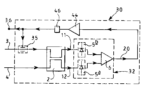
Figure 4 shows a manually operated optical phase detector 30 in accordance
with one aspect of the present invention. The optical phase detector 30 has a
linearised response, and comprises a voltage controlled electro-optic phase
modulator 35 in one of the input paths 3,4 (input 3 in Figure 4). The electro-
optic phase modulator 35 has a substantially linear variation of optical phase
with applied voltage 36. If this voltage were manually (or automatically)
adjusted to maintain a constant (ideally zero) output 20 from the differential
amplifier the voltage 36 applied to the modulator 35 gives a direct linear
measure of the relative phase between the optical inputs 3,4. In practice,
automatic, as opposed to manual, adjustment of the applied voltage 36 would
be highly desirable. The range of electro-optic phase modulation may be at
least 360 .
The electro-optic phase modulator 35 may be placed in the path of one of the
inputs 3,4 to the optical phase detector 1. The output 20 from the
differential
CA 02343780 2001-03-12
WO 00/17613 PCT/GB99/03179
-19-
amplifier 6 is then set at a constant level by applying the appropriate
voltage to
the voltage-tuned electro-optic phase modulator. Preferably, the output 20 may
be maintained at zero volts which makes the measurement insensitive to
amplitude variations.
As the response of electro-optic phase modulators is very linear, in
particular
lithium niobate and lithium tantalate devices, the voltage required to set the
differential amplifier output to zero gives a useful measure of the relative
phase. The frequency response of the electro-optic phase modulator may,
typically, be between 1MHz and 1 GHz. For some applications, it may be
desirable to include an electro-optic phase modulator having a frequency
response exceeding 1 GHz. The voltage adjustment may be made manually, or
by means of an electrical feedback loop. Including the electro-optic phase
modulator provides the advantage that the phase detector is linearised (i.e.
the
voltage required to tune the electro-optic modulator in order to maintain the
differential amplifier at a constant voltage is directly proportional to the
measured phase difference) and the operating range is extended to at least 360
.
If the difference signal is maintained close to zero the optical phase
detector
has the further advantage that it is insensitive to amplitude variations in
the
input optical signals. Additionally, as the frequency response of the electro-
optic modulator 35 is very fast, the phase measurement can be determined
rapidly. The phase detector is therefore suitable for dynamic measurements. In
practice, the speed of response of the optical phase detector may be limited
by
the detector or feedback electronics.
In an alternative embodiment, the electro-optic phase modulator may take the
form of an optical fibre, on which a piezoelectric film is deposited, for
example
ZnO, the optical fibre being stripped of its outer cladding. By applying a
CA 02343780 2001-03-12
WO 00/17613 PCT/GB99/03179
-20-
voltage across the ZnO film on the fibre, a phase shift can be induced. This
embodiment may be advantageous as it avoids the size, cost and insertion loss
of an integrated optic phase shifter.
Figure 5 shows an embodiment of the linearised optical phase detector 30
which includes an electronic feedback loop, comprising a feedback amplifier
44 and filter 46. As shown in the figure, the feedback amplifier 44 and filter
46
may be separate components, but alternatively the filter may be derived from
the amplifier characteristic itself which is carefully designed to be stable.
The
voltage 36 applied to the electro-optic phase modulator 35 provides the
output,
which is linearised. The advantage of this embodiment of the phase detector is
that it removes the need for a human operator and is relatively fast and
accurate
in operation. Figures 6(a) and 6(b) show experimental results obtained using
the device shown in Figure 5. The measurements were obtained directly from a
Tektronix 2430 digital oscilloscope. The solid lines are the best fits to the
measured points. This characteristic may be compared with the nonlinear
(sinusoidal) response of Figure 3.
The optical phase detector shown in Figure 5 also provides an advantage over
that shown in Figure 1 as it has an extended operating range. In the optical
phase detector shown in Figure 1, the output is nonlinear (sinusoidal) and the
greatest unambiguous operating range is therefore 180 . The optical phase
detector of the present invention has a very linear response and the range can
be extended to at least 360 , as shown in Figure 6(b). It is particularly
important, for example, to have an operating range greater than 360 in
vector
voltmeter or network analyser applications, as will be described hereinafter.
CA 02343780 2001-03-12
WO 00/17613 PCT/GB99/03179
-21-
A circuit diagram of part of the optical phase detector 30 is shown in Figure
7.
In a non-linear optical phase detector 1(i.e. as shown in Figure 1), the
detectors
5a,5b are be arranged such that the net output signa120 varies sinusoidally
about zero depending on the relative phase between the inputs 11,12. Hence a
bipolar signal 20 is output from the detector (as shown in Figure 3).
Typically,
the detectors 5a,5b may be reverse biased PIN devices, although any low noise
detector may be used. Commercially available optical detectors GAP 60 or
GAP 100 may be suitable devices. The value of resistor R, (as shown in Figure
7) determines the gain and hence the peak to peak bipolar output voltage.
Typically, the voltage (+V, -V) applied across the detectors may be 9 Volts.
If the photodetectors 5a, 5b are not quite identical, means for equalising the
sensitivity of the photodetectors may be included in the phase detector. It
has
been found that the bias voltage on one or both detectors may be varied in
order to provide a fine adjustment to photodetector sensitivity.
The linearised optical phase detector 30 provides a DC output voltage which is
a measure of the phase difference between the two inputs. This cannot be
achieved with conventional electrical phase detectors due to the high optical
frequencies of the inputs. Furthermore, the optical phase detector of the
invention is advantageous as the output occurs as a direct electrical signal
giving a measure of phase difference. The detector may therefore be used in a
high accuracy displacement measurement apparatus for measuring
displacements of the order of a few nanometres. This may be of particular use
in laser metrology. For example, the output from the optical phase detector
provides a measure of the phase difference between two input signals derived
from the same, stable laser, where one of input signals is reflected from a
displaced surface or object. The phase difference may be used to provide an
CA 02343780 2001-03-12
WO 00/17613 PCT/GB99/03179
-22-
indication of the displacement of the surface or object. The input laser may
be
stabilised by the laser stabilisation apparatus of the invention which will be
described later.
The optical phase detector may also be used to phase lock two independent
lasers, for example a high powered tuneable laser and a low power stable
laser.
This is achieved by inputting laser outputs from two different lasers to the
optical phase detector (i.e. as inputs 3 and 4 shown in Figure 1 and 4) and
employing a feedback loop connected to the tuning point of the tuneable laser.
The characteristics of the optical phase detector of the present invention may
also be exploited in a frequency discriminator. In general terms, a frequency
discriminator employs an input signal of ideally constant amplitude and
produces an output voltage proportional to, or dependent on, the amount by
which the input frequency differs from a fixed frequency.
Referring to Figure 8, there is shown a laser stabilisation apparatus in
accordance with another aspect of the invention, as will be described
hereinafter. The parts of the apparatus enclosed within the dotted line,
referred
to generally as 60, form a frequency discriminator comprising an optical phase
detector 1(as shown in Figure 1) and a 50/50 fibre optic directional coupler
41
for receiving an output 42 from a laser 43. The discriminator 60 also
comprises
means for introducing a relative delay between the two output signals 52, 53
from the coupler 41. Preferably, this may be achieved by means of two lengths
of optical fibre 50,51, each for receiving one of the output signals 52,53
from
the coupler 41, one optical fibre being longer than the other so as to
introduce a
relative delay. In practice it is convenient if one of the lengths of optical
fibre is
very short. Preferably, the one or more length of optical fibre 50,51 may be
CA 02343780 2001-03-12
WO 00/17613 PCT/GB99/03179
-23-
temperature-stable optical fibre which gives the apparatus improved
temperature stability. Alternatively, or in addition, to achieve temperature
stability, the apparatus may be housed in a temperature-stable oven. A
polarisation modulator, such as an in-fibre polarisation modulator, may be
included in either one or both pathways 50,51, as discussed previously.
It will be appreciated that, although the electro-optic modulator 35 within
the
optical phase detector is not shown in the frequency discriminator 60 forming
part of the laser stabilisation apparatus in Figure 8, the electro-optic
modulator
35 may be included, and may be particularly important in other applications of
the discriminator.
The function of the frequency discriminator 60 is to split the output of a
laser
43 into two substantially equal output beams 52,53 by means of the first
coupler 41, delay one signal relative to another and then measure the optical
phase difference between the two signals 52,53. This may be done by means of
the optical phase detector of the present invention. It cannot be done using
conventional electrical phase detectors as the optical frequencies in question
are far too high.
One output 53 from the first coupler 41 is connected through an optical fibre
51
to a second 50/50 fibre optic coupler 2, which forms part of the optical phase
detector 1. The other output 52 is passed through the longer optical fibre
(i.e. a
delay line 50) before connection to this coupler 2. Alternatively, another
type
of delay medium may be used, for example integrated optic delay lines. As
discussed previously, the outputs from the second coupler 2 (incorporated
within the optical phase detector 1) vary in level depending on the relative
phase of the input signals to the coupler 2. The optical phase detector 1
CA 02343780 2001-03-12
WO 00/17613 PCT/GB99/03179
-24-
therefore provide a DC output voltage which depends on the relative phase
between of the two inputs. For example, if the delay line has a delay of Td
seconds, the phase shift will vary by 2x radians for every 1/ Td change in the
input laser signal frequency. The frequency discriminator 60 therefore
operates
with a control characteristic which repeats every 1/Td change in frequency. As
shown in Figure 3, the discriminator output voltage 20 (i.e. the output
voltage
from the differential amplifier 6) varies sinusoidally with the relative
optical
phase of the two input signals.
If the optical phase detector is arranged to operate around OV, a bipolar
output
signal is produced, as described previously. If the input frequency to the
first
coupler varies in time, this will result in a change in the bipolar output
signal.
For an increased laser output frequency, the bipolar output signal from the
discriminator will be of one polarity and for a decreased laser output
frequency
the signal from the discriminator will be of the opposite polarity. The
magnitude of the bipolar output depends on the degree of phase shift and hence
the frequency shift of the input laser. Typically, the peak to peak voltage
may
be in the range between +/- 0.1-10 V.
A frequency discriminator has useful applications itself, for example to
measure the output spectrum of a laser. The electrical output from the
frequency discriminator 60 may be used to provide a measure of the optical
frequency (or wavelength) of an input laser as long as the relative delay
between fibres 50 and 51 is known and is substantially stable. This does
provide a frequency (or wavelength) measurement, although it is an ambiguous
one as the phase is only measured modulo 2n. A further ambiguity arises from
the sinusoidal response shown in Figure 3, as the maximum unambiguous
phase range is n. This is, however, a useful measurement over a small
CA 02343780 2001-03-12
WO 00/17613 PCr/GB99/03179
-25-
frequency range. The delay line length may be adjusted to set the required
sensitivity. Ideally, the phase excursion will be kept to within a few degrees
around zero to maintain linearity. Alternatively, and preferably, the
linearised
optical phase detector 30 (as shown in Figure 5) may be employed within the
discriminator 60 to maintain linearity and range.
The bipolar output signal of the frequency discriminator may also be exploited
as a means of correcting for any phase deviation in the laser output 42.
Referring again to Figure 8, this correction process may be achieved by means
of a laser stabilisation apparatus (within outer dashed line and referred to
generally as 70). The laser stabilisation apparatus 70 comprises the frequency
discriminator 60 and a feedback circuit. The laser output 42 to be stabilised
is
split into two signals, preferably of equal amplitude, by the coupler 41.
Preferably, the output 42 from the laser 43 is passed through an optical
isolator
62 to remove the detrimental effects of any light reflected back into the
laser
43. The output 20 from the discriminator 60 is then fed back to the laser 43,
so
as to vary its frequency, through the feedback circuit. It is important in the
laser
stabilisation apparatus 70 that the discriminator output 20 is a bipolar
output so
that a frequency shift in either direction can be corrected to stabilise the
laser
output 42.
The feedback circuit comprises a control loop amplifier 72 and a loop filter
74.
The output 20 from the discriminator 60 is amplified by the control loop
amplifier 72 and is then passed through the loop filter 74 to produce an error
signal. This error signal may then be used to control the frequency of the
laser
43. An error signal of the correct sign is applied to the frequency control
point
so as to reduce frequency fluctuations and, hence, improve the phase noise
spectrum. The "stabilised" output 76 from the laser may be taken from the
CA 02343780 2001-03-12
WO 00/17613 PCT/GB99/03179
-26-
apparatus by using an additional coupler 78 located in the path before the
discriminator 60.
In the case of a semiconductor laser, such as a laser diode, the feedback may
be applied by varying the laser current, as the laser frequency varies with
current, the dominant mechanism being the change in refractive index, due to
changes in the effective refractive index with current injection.
Alternatively, it
is be possible to build into a laser cavity a reverse-biased section such that
it
does not absorb light but changes refractive index with an applied voltage
which derives from the discriminator output.
The function of the laser stabilisation apparatus is to reduce the output of
the
differential amplifier to substantially zero, thus maintaining the laser
frequency
at one of the stable operating points of the frequency discriminator. The
laser
will eventually lock to the nearest stable operating point and, once lock is
achieved, the system maintains control of the laser frequency at that
particular
frequency. The system may therefore be used to improve the spectral stability
of the laser.
Measurements have been obtained for a Lightwave Electronics Series 123
Fibre-coupled Diode-pumped solid state non-planar ring laser controlled by a
Series 2000 LNC Laser and Locking Accessory (LOLA). The laser had a
frequency control input with a tuning range in excess of 30 MHz and a
bandwidth of 100 kHz for small modulation indices and had a quoted linewidth
of 5kHz. Figure 9(a) shows the low frequency spectrum measured at the output
from the discriminator and shows the phase noise (dBc/Hz) as a function of
offset frequency in free running conditions (o) (i.e. measuring the laser
output
directly) compared to the phase noise measurements obtained when using the
CA 02343780 2001-03-12
WO 00/17613 PCT/GB99/03179
-27-
laser stabilisation apparatus 70. The measurements show a considerable
improvement in the close-in phase noise performance for a laser which already
has a quoted linewidth of around 5 kHz (i.e. spectrally pure). In these
measurements the differential delay was I s. Additionally, Figure 9(b) is a
similar spectrum obtained for an E-Tek DFB laser, comparing the phase noise
(dBc/Hz) as a function of offset frequency in free running conditions (i.e.
open
loop, measuring the laser output directly) compared to the phase noise
measurements obtained when using the laser stabilisation apparatus 70. In
these
measurements, the differential delay was 5 ns.
As lasers with high spectral purity tend to be relatively expensive, the
system
enables less expensive and spectrally less pure lasers to be improved
relatively
cheaply and easily. The improvement of low cost semiconductor lasers may
therefore also be achieved using this system.
The most common, cheap and widely used laser is a laser diode but it has a
particularly poor spectral stability, especially in the case of Fabry-Perot
etalon
designs. The laser stabilisation apparatus may be therefore be particularly
useful for improving the spectral stability of these devices, as well as DFB
lasers. It may also be used to improve stable lasers which is also very
useful,
for example in high resolution spectroscopy and in frequency standards. In
particular, the degree of phase noise improvement which may be obtained is
dictated by the choice of the delay time. Typically, the delay line may
introduce a relative delay of up to 10 s between the output signals from the
first coupler, depending on the range and sensitivity needed to give the
required
degree of spectral improvement. The delay time must also be chosen so that the
open loop gain of the discriminator is reduced to well below unity at
frequencies approaching the reciprocal of the delay time. For example, for a
CA 02343780 2001-03-12
WO 00/17613 PCT/GB99/03179
-28-
delay line of 1 s, the open loop gain of the discriminator should be well
below
unity for input frequencies of around 1 MHz. If lasers, such as laser diodes,
have a high noise level at greater offset frequencies a wideband loop (and
short
delay) must be used. Thus, for lower performance lasers, much higher loop
bandwidths are required. A lower discriminator gain may be compensated for
by increasing the gain of the control loop amplifier. Johnson noise from the
amplifiers is likely to be the limiting factor in this gain increase.
Usually, laser diodes have two outputs, one from each facet, or mirror, the
second output usually being used to monitor power level. However, it may be
possible to use the second output as the input to one of the two optical
detectors, hence alleviating the need for the first coupler. However, this
embodiment may only be used if the two outputs from the laser are strongly
correlated.
In an alternative embodiment of the invention, the laser stabilisation
apparatus
may comprise two or more loops in parallel. For example, a second output may
be taken from the laser 43, or a split signal from output 42, and fed through
a
second loop having a different gain bandwidth from the first feedback loop.
Each loop may then be used to feed back and control the input laser. For
example, different feedback signals from each loop may be used to control
separate temperature and frequency controls points on the laser, or may be
combined and fed back to the same control point on the laser. Alternatively,
the
output from the discriminator 60 may be split, with one split signal feeding
back to the laser 43 through one control loop amplifier and loop filter
arrangement, and the other signal feeding back to a different control port on
the
laser via a second control loop amplifier and loop filter.
CA 02343780 2001-03-12
WO 00/17613 PCT/GB99/03179
-29-
The laser stabilisation apparatus of the present invention is advantageous as
it
is an in-fibre system and is therefore is less susceptible to external
factors, such
as vibration, temperature changes and dust, than a free space system. This is
especially true if temperature-stable optical fibre is used, as discussed
previously. The apparatus may also have a higher effective Q-value compared
to that which may be obtained with the known device, the Q-value depending
on the length of fibre and therefore, indirectly, on the original laser
stability.
Furthermore, the length of the fibre optic delay line, and hence the relative
delay may be selected in order to vary the sensitivity and range depending on
the degree of spectral improvement required. The apparatus may be particularly
useful for stabilising the output from laser diodes and other forms of laser,
for
example to allow them to be used more effectively in fibre optic
communications systems.
Referring to Figure 10, it is sometimes desirable to frequency modulate a
laser
e.g. to transmit information, or slowly sweep the frequency of the stabilised
laser. This may be done by introducing an electro-optic phase modulator 80 or
a differential amplifier arrangement 82,83, as will be described hereinafter.
For
example, an electro-optic phase modulator 80 may be included in the laser
stabilisation apparatus 70, for example in either of the delay lines 50,51
(delay
line 50 in Figure 10). Alternatively, the electro-optic phase modulator 80 may
form part of the optical phase detector itself, as described hereinbefore. In
use,
the laser frequency may be modulated by first stabilising the laser 43 so that
the
output from the differential amplifier 6 of the optical phase detector 1 is
maintained at, say, zero volts and then by applying an appropriate voltage
waveform to the electro-optic phase modulator 80. The linearity of the
phaseshift in the electro-optic phase modulator ensures a high fidelity
frequency-modulated output.
CA 02343780 2001-03-12
WO 00/17613 PCT/GB99/03179
-30-
An application of this technique may be to sweep the input laser frequency
slowly through an atomic absorption line to make precise measurements of the
lineshape. This may be especially useful in the measurement of very narrow
lines due to the spectral stability of the laser.
The apparatus of Figure 10 may also be used to convert the stabilised laser
output 76 into a stabilised optical synthesizer. In this application, the
voltage
waveform applied to the phase modulator 80 may have the form of a
"SAWTOOTH" voltage waveform, in which the phase is swept slowly and
linearly over 360 and then rapidly switched back through 360 . However,
other waveforms may also be used for this application. Suitable waveforms
include those which slowly increase with time and then rapidly decrease to the
initial voltage level. The increasing level does not therefore have to vary
linearly with time, as in the case of a SAWTOOTH waveform. For the purpose
of this specification, any waveform having a slowly increasing voltage level
with time followed by a rapid switch back through 360 (in the opposite
direction) shall be referred to as a SAWTOOTH-like waveform. Such
waveforms include waveforms in which the slowly increasing voltage level is
of stepped form. The SAWTOOTH-voltage waveform may or may not be
swept linearly over 360 . Typically, the timescale over which the waveform is
switched back through 360 will be of the order of nanoseconds.
By way of example, Figure 11(a) shows an example of a SAWTOOTH voltage
waveform (as a function of time) which may be applied to the electro-optic
phase modulator 80 for this purpose and Figure 11(b) shows the corresponding
change in phase of the modulator 80 with time. During the switching process
the laser frequency first follows the slow change in voltage waveform (i.e.
modulator pulse) but does not follow the rapid reduction in phase by 360
CA 02343780 2001-03-12
WO 00/17613 PCT/GB99/03179
-31-
because the feedback loop filter (i.e. 72, 74) will not respond at this speed.
In
other words, the switch through 360 degrees has no net effect because the
laser and feedback loop are unable to respond to a rapid change. In addition,
the output of the optical phase detector 1 is unaffected by the change of
phase
of 360 as its response is periodic with 360 (as shown in Figure 3). The
laser
output 76 therefore remains at the new frequency. This process may be
repeated many times to cover the full tuning range of the laser. A change of
frequency in the opposite direction can be achieved by reversing the voltage
waveform slope.
Using the apparatus shown in Figure 10, the stabilised laser output 76 can be
controlled to any required frequency by applying an appropriate voltage 86 to
the phase modulator 80. In some circumstances this is useful, for example it
allows the response over a small frequency range to be measured with a
continuous linear sweep rather than as a series of frequency intervals.
As an alternative to an electro-optic phase modulator, a differential
amplifier
may be included in the feedback loop to provide a similar laser-tuning
function.
For example, referring to Figure 10, a differential amplifier 82 may be
included
in the signal pathway at X. Altematively, the differential amplifier may form
part of the control loop amplifier 72 itself or may be placed in the path
prior to
the control loop amplifier 72. In either of these arrangements, rather than
maintaining the output 20 from the discriminator 60 at OV, the input 83 to the
differential amplifier 82 may be set to a constant value say, 1 V. The
differential amplifier 82 in the feedback loop measures the differential
between
1 V and the output voltage from the discriminator 60 after passing through the
control loop amplifier 72 and loop filter 74. The differential output 84 is
then
fed back to control the input laser 43 whose frequency changes to make the
CA 02343780 2001-03-12
WO 00/17613 PCT/GB99/03179
-32-
output of the loop filter approach 1 V. This would also allow a frequency
modulation capability. By this means the laser may be swept in frequency
enabling, for example, measurement of narrow spectral line widths and shapes.
It will be appreciated that, if the differential amplifier forms part of the
control
loop amplifier 72 itself or is placed in the path prior to the control loop
amplifier 72, the operating characteristics will be different from an
arrangement in which the differential amplifier is located at X, as the
amplifier
is located on a different side of the filter in each case. The use of the
differential amplifier 82 instead of the electro-optic phase modulator 80 is a
cheaper approach and may be improved by using a linearised optical phase
detector (as shown in Figure 5) in place of an optical phase detector having a
nonlinear response (as shown in Figures 1, 8 and 10). The use of the electro-
optic phase modulator 80 is the preferred approach, however, and has been
built and tested in the laboratory.
Figure 12 shows the results obtained using the optical synthesizer shown in
Figure 10, including the electro-optic modulator 80. The figure comprises
eight
spectra measured on an electrical spectrum analyser by mixing the optical
synthesizer output at 76 with the output of a stable fixed laser frequency. In
this
demonstration the discriminator differential delay is 1 microsecond, so
successive laser frequencies are 1 MI-iz apart. However, to provide an
intelligible plot the spectra were taken every ten "cycles" of the phase-
modulator (i.e. every ten SAWTOOTH waveform cycles and 10 MHz
intervals). The scales on the plot shown in Figure 11 are single sideband
phase
noise dBc/Hz at 10 dB/division (vertically) and 10 MHz/division
(horizontally).
CA 02343780 2001-03-12
WO 00/17613 PCT/GB99/03179
-33-
Although Figure 12 shows every 10'h member of a "comb" of frequencies
spaced by 1 MHz, it will be appreciated that the synthesizer may be tuned to a
frequency between adjacent comb frequencies by applying the appropriate
voltage to the modulator 80. For example, 16 steps may be provided by using a
computer processor and a 4-bit digital to analogue converter (DAC), whereby
the DAC converts digital controls from the computer processor into an
analogue voltage to be applied to the electro-optic phase modulator 80. This
would introduce phase steps of 22.5 , the 16th step being 360 corresponding
to
a 1 MHz step in Figure 12.
The optical frequency synthesizer may also be employed in combination with a
diffractive element, such as a zone plate lens or a diffraction grating, to
provide
a programmable function. For example, the output from the optical frequency
synthesizer may be used to illuminate a phase reversal zone plate lens, the
focus of which is dependent on wavelength. By varying the voltage applied to
the electro-optic phase modulator 80 forming part of the optical frequency
synthesizer, the wavelength of the output from the synthesizer can be varied
and, thus, the focus of the lens can be varied. This may be used, for example,
to
access different layers of an optical memory, such as a compact disc.
Alternatively, the optical frequency synthesizer may be used to illuminate a
diffraction grating to "steer" the laser output. This may be used, for
example, as
a means of accessing a hologram.
Figure 13 shows how the linearised optical phase detector 30 of the present
invention (as shown in Figure 4) may be used in sensor applications where the
measurand modifies the properties of optical fibre 50 (or 51). For example,
the
sensor may be used to measure any one of temperature, pressure, strain,
displacement, vibration, magnetic fields or magnetic field gradients, electric
CA 02343780 2001-03-12
WO 00/17613 PCT/GB99/03179
-34-
current, electric field, voltage, chemical species, biochemical parameters,
medical parameters or communications characteristics. For example, referring
to Figure 13, if the output 20 from the differential amplifier 6 is set to
zero
volts by varying the voltage 36 applied to the electro-optic phase modulator
35,
any variation in temperature (or other measurand) of the optical fibre delay
line
50 will give rise to a change of phase, hence the output from the phase
detector
will vary. The amount by which the voltage 36 on the electro-optic modulator
35 varies to maintain the output 20 from the differential amplifier 6 at zero
(or
very close to zero) provides an indication of the variation in temperature (or
other measurand). The output of such a measurement will typically be very
linear.
Although it may be advantageous to use temperature stable optic fibre
throughout the sensor, for a temperature sensor application the use of
temperature stable optical fibre for the delay line 50 is not appropriate. In
such
schemes a stable input laser 43 should be used. A stabilised laser input may
be
achieved by using the laser stabilisation apparatus of the present invention,
as
described previously.
In the sensor application, as distinct from the frequency discriminator
application, the two optical fibres 50,51 may have substantially the same
delay,
rather than having a relative delay therebetween. In some circumstances this
may be of benefit. For example, if measuring the pressure on fibre 50, any
temperature variation will be common to both fibres 50 and 51 and will
therefore cancel if the delays are equal. Similarly, the system can employ a
less
stable laser. It is also possible to implement the sensor as a free-space
arrangement, rather than an in-fibre apparatus, as will be described later.
CA 02343780 2001-03-12
WO 00/17613 PCT/GB99/03179
-35-
The optical frequency synthesizer of the present invention may also be
employed in an improved form of distributed fibre optic sensor. Conventional
fibre optic sensors employ an array of Bragg gratings distributed along the
length of the optical fibre. The individual gratings can then be interrogated
by
means of a tuneable laser, tuned close to the Bragg frequencies. By employing
the optical frequency synthesizer of the present invention in a distributed
fibre
optic sensor arrangement, advantages are obtained due to the improved
stability
of the laser and, in addition, because the laser frequency can be set with
high
accuracy. As a consequence, it would be possible to implement such a sensor
with an increased number of Bragg gratings, permitting a greater number of
interrogation points to be used. An additional advantage of this fine-tuning
capability is that it enables the overall distortion of a grating to be sensed
at
narrow frequency intervals. For example, the reflection bandwidth of a
periodic
grating will increase if different paths are affected differently by the
measurand.
Referring to Figure 14, the linearised optical phase detector (as shown in
Figure 5) may also be employed in an optical vector voltmeter 90 which
operates at optical frequencies. The optical vector voltmeter comprises a
linearised optical phase detector 30 (enclosed within the dashed line) which
has
an operating range of at least 360 . The function of the vector voltmeter is
to
take two inputs 92,94 and to generate two outputs, one of which (output 100)
is
the absolute amplitude of the unknown input and the other of which (output
102) is the phase of the unknown input signal 92 relative to that of the
reference input 94. The unknown input signal 92 is split and one part is input
to
a detector 96 to provide the amplitude output 100. Typically, the detector
current varies linearly with optical intensity, from which the amplitude is
readily derived. The second part 93 of the split input signal is input to the
CA 02343780 2001-03-12
WO 00/17613 PCT/GB99/03179
-36-
linearised optical phase detector 30, along with a reference input signal 94.
The
output from the differential amplifier 6 is fed back to the electro-optic
phase
modulator 35 via a feedback amplifier and filter 44, 46. The voltage applied
to
the electro-optic phase modulator 35 is adjusted, via the feedback loop, to
maintain the differential amplifier 6 at a constant value, very close to zero.
The
electro-optic phase modulator input voltage provides the phase output 102.
This gives a direct linear measure of the relative phase between the unknown
input 92 and reference input 94.
Figure 15 shows a schematic diagram to illustrate how the optical vector
voltmeter 90 shown in Figure 14 and the apparatus shown in Figure 10 may be
employed in an optical network analyser for transmission measurement of a
system under test (e.g. an optical fibre of unknown properties). The optical
network analyser is similar to the optical vector voltmeter, except that it
provides a synthesised frequency input to the system under test 110 and
typically may measure the transmitted amplitude and phase of the system 110
at a series of frequencies as the optical frequency synthesizer 108 is stepped
and/or swept in frequency. As in the optical vector voltmeter, the linearised
optical phase detector is arranged to have an operating range of at least 360
.
The optical network analyser of the present invention is not limited to
including
an optical frequency synthesizer as herein described, and may include any
optical frequency synthesizer apparatus.
Referring to Figure 15, the optical network analyser comprises an optical
synthesizer 108 whose output is split. The operation of the optical
synthesizer
is described above with reference to Figure 10. The stabilised laser output 76
shown in Figure 10 provides the optical synthesizer output to be split. One
part
of the split signal 76a is transmitted to the system under test 110 and is
CA 02343780 2001-03-12
WO 00/17613 PCT/GB99/03179
-37-
transmitted 92 to an optical vector voltmeter 90 (input SYS) as described
above
(i.e. input signal 92 in Figure 14 is transmitted to the optical vector
voltmeter
90). The other part of the split signal 76b is input to the reference port
(input
REF) of the optical vector voltmeter 90 (i.e. reference signal 94 in Figure
14).
The outputs 100, 102 from the optical vector voltmeter 90 fonn the network
analyser outputs. Typically, measurements may be made over a range of optical
frequencies (by sweeping and/or stepping the optical synthesizer, as described
previously). Other properties, such as group delay, can be calculated
digitally
using the phase and frequency measurements. Results may be displayed on a
VDU, or in digital form.
A variety of other measurements are also possible. For example the amplitude
and phase of signals reflected by a system under test 110 may be measured
using the optical network analyser shown in Figure 16 which is essentially a
rearrangement of the optical network analyser shown in Figure 15. In this
embodiment, the input signal 76 is transmitted (via a directional coupler 112)
to the system under test I 10 and provides a reference signal (REF) to the
optical vector voltmeter 90. However, in this embodiment, the signal 114
reflected back from the system 110 provides the other input to the optical
vector voltmeter 90 via the coupler 112. In practice, the system will also be
terminated by a load, T.
It may be preferable to use temperature stable fibres throughout the apparatus
of the present invention (e.g. the laser stabilisation system, the optical
synthesizer, the frequency discriminator, the optical vector voltmeter, the
optical network analyser, the optical phase detector or in sensor
applications),
both for connecting optical fibres used throughout the apparatus as well as
the
one or more delay lines 50,5 1. Temperature stable fibre is commercially
CA 02343780 2001-03-12
WO 00/17613 PCT/GB99/03179
-38-
available. The use of temperature stable fibres enables the frequency of the
laser output to be stabilised to a higher degree as changes in ambient
temperature will have a reduced effect on the optical delay paths.
Alternatively,
the fibres may be placed in a temperature controlled environment, or the
optical
path length may include an auxiliary temperature dependent path in series with
the fibre in order to maintain a constant delay period. Alternatively, or in
addition for extra stability, the apparatus may be operated in a temperature
stable oven. Polarisation maintaining optical fibre, temperature stable single
mode optical fibre or temperature stable polarisation maintaining optical
fibre
may also be used.
Although most optical measurements of the kind herein described are
invariably performed using fibre optics, the medium used in fibre optic
communications, there are some circumstances in which applications of the
kind described may be performed using free space optics. The apparatus shown
in the various aspects of the present invention can be implemented in this
way.
For example, in gas sensor applications the presence of a gas species in air
can
be detected through dispersion associated with an absorption line since the
dispersion causes an actual phase shift. Referring to Figure 17(a), the
apparatus
shown in Figure 13 is alternatively implemented by employing laser beams in
free space (as opposed to in-fibre) by collimating and refocusing the
radiation
with lenses.
The sensor shown in Figure 17 comprises an input coupler 178, or beam
splitter, for receiving a beam of laser radiation 76 and providing two output
beams of radiation, lenses 180,182 to perform beam collimation and lenses
190,192 to refocus the beams of radiation into the input paths 3,4 of the
phase
detector shown in Figure 5. As discussed previously, in this application the
two
CA 02343780 2001-03-12
WO 00/17613 PCT/GB99/03179
-39-
free space paths 194 and 196 (corresponding to paths 50 and 51 in Figure 13)
may be of substantially equal length, one containing pure air (path 196) and
one being contaminated by gas (path 194). Typically, the paths 194,196 may be
hollow tubes.
In an alternative embodiment, with reference to Figure 10, the optical phase
detector forming part of the discriminator in the laser stabilisation
apparatus
may include a second electro-optic phase modulator in the path of the input 4.
In this case, a DC voltage may be applied to the first electro-optic phase
modulator 35 to set the frequency of the laser, and an RF voltage may be
applied to the second electro-optic phase modulator. This provides a
convenient way of applying RF modulation to the laser frequency. Other
benefits may also be obtained by including a second electro-optic phase
modulator in the apparatus. The optical phase detector in Figures 4 and 5 may
also include a second electro-optic phase modulator in the path of the input
signal 4. In this way, for example, the "tuning" range may be extended, and
even doubled, by arranging the electro-optic phase modulators in such a way
that they both contribute to the tuning range.
It will be appreciated that, for the purpose of this specification, the phrase
"optical" is not intended to be limited to visible wavelengths, and includes,
for
example, infra red wavelengths and ultra violet wavelengths.