Note: Descriptions are shown in the official language in which they were submitted.
CA 02344076 2001-11-14
SURFACE MOUNTING SURGE ABSORBER AND SURFACE MOUNTING CAP FOR SURGE
ABSORBER
BACKGROUND OF THE INVENTION
1. Field of the Invention
The present invention relates to a surface mounting surge
absorber and a surface mounting cap for a surge absorber, and in
particular to an improved surface mounting surge absorber and
surface mounting cap for a surge absorber which can be incorporated
onto a printed substrate or the like with high mounting density.
2. Description of the Related Art
High voltage surges such as stray waves, noise, and
electrostatic disturbances are deeply-rooted obstacles to the most
up-to-date electronic devices. In particular, high voltage pulse
waves cause erroneous operations of semiconductor elements in
electronic devices, and in some cases, may even destroy the
semiconductors or the devices themselves. Various types of surge
absorbers are used in order to prevent such high voltages from
flowing into the electric devices.
A surge absorber has been disclosed by the inventors which
has a simple structure and shows good characteristics , in Japanese
Patent Laid-Open Publication No. 2000-268936. With this surge
absorber, a wide range of surge characteristics can be covered with
an inexpensive structure and a compact shape.
However, when such a surge absorber is to be incorporated onto
1
CA 02344076 2001-11-14
a printed substrate, the lead lines provided at both ends of the
surge absorber are inserted into a through hole of the printed
substrate and then soldered. Because of this, in the prior art,
the soldering operation of the surge absorber onto the substrate
required many steps . Also , because the printed substrate must be
provided with a through hole, a two-sided substrate could not be
used.
In order to handle the above problem, there is a strong demand
for a surge absorber which can be surface mounted. With a surface
mounting surge absorber, the incorporation operation onto the
printed substrate as described above can be significantly
simplified, and such a surge absorber enables the 'usage of two-sided
substrates . Moreover, the overall device can be densified and the
surge absorber can be mounted onto the print substrate with high
density. Because of this, the surge absorber is advantageous in
reducing the size of the electronic devices.
The present invention is conceived to solve the above
described problem in the prior art and one object is to provide
a surge absorber with a simple structure which can be surface
mounted.
SUMMARY OF THE INVENTION
In order to achieve the object, according to one aspect of
the present invention, there is provided a surface mounting surge
absorber comprising a surge absorber element, constructed by
0
CA 02344076 2001-11-14
affixing discharge electrodes with lead lines on both internal ends
of a cylindrical housing and having a chamber gap within the housing
between said discharge electrodes adjusted by the fixed positions
of the discharge electrodes so that desired discharge
characteristics are obtained, and surface mounting caps placed on
both ends of the cylindrical housing, wherein the surface mounting
cap comprises a flange section for grabbing the outer peripheral
end of the cylindrical housing and acting as a solder receiving
section when the surface mounting cap is mounted on a surface, a
clear hole to which the .lead line is inserted, and a binding section
provided around the clear hole for snapping onto the lead line.
According to another aspect of the present invention, there
is provided a surface mounting cap to be placed on the ends of a
surge absorber element, the surface mounting cap comprising a flange
section for grabbing the outer peripheral end of the surge absorber
element and acting as a solder receiving section when the surface
mounting cap is mounted on a surface, a clear hole to whi<:h the
lead line of the surge absorber element is inserted, and a binding
section provided around the clear hole for snapping onto the lead
line .
BRIEF DESCRIPTION OF THE DRAWINGS
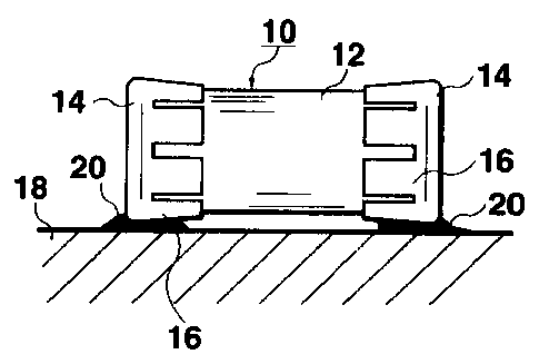
Fig. 1 is a descriptive figure showing a condition where a
surface mounting surge absorber according to the present invention
is soldered and fixed onto a printed substrate
3
CA 02344076 2001-11-14
Fig. 2 is a cross sectional diagram of the surge absorber
element used in the present invention.
Fig. 3 is a cross sectional diagram showing a preferred
embodiment of a surface mounting cap according to the present
invention.
Fig. 4 is a front view of the cap bottom section seen from
the axial direction of the surface mounting cap depicted in Fig.
3.
Fig. 5 is a cross sectional diagram showing a condition where
coating is applied to the surface mounting surge absorber according
to the present invention.
DESCRIPTION OF PREFERRED EMBODIMENTS
Fig . 1 shows a condition where a surface mounting surge
absorber according to the present invention is mounted on a printed
substrate. The surge absorber element 10 comprises a cylindrical
housing 12 , as will be described later, and the cylindrical housing
12 is provided with surface mounting caps 14 placed on the two ends .
Each surface mounting cap 14 is electrically connected t:o the
discharge electrode of the surge absorber element 10 via a lead
line, as will be described later. The surface mounting cap 14 has
a flange section 16 for grabbing the outer peripheral end of the
housing 12 and acting as a solder receiving section when the surface
mounting cap 14 is mounted on a surface. As shown in Fig. 1, both
flange sections 16 of the surface mounting caps 14 are firmly fixed
4.
CA 02344076 2001-11-14
and connected to a predetermined wiring section of the print
substrate 18 by solder 20.
Fig. 2 shows the detailed structure of the surge absorber
element according to the present invention. The cylindrical
housing 12 is a glass diode container of international standard
DO-41 type (with an inner radius of 1.53 mm) and the inner radius
is uniform in the axial direction.
A pair of discharge electrodes 22 are inserted to the inside
of the cylindrical housing 12, and are molded and fixed to the
cylindrical housing 12 via sealing spacers 23. During the molding
and fixing operations, the fixed positions of the discharge
electrodes 22 within the cylindrical housing 12 can be arbitrarily
adjusted to arbitrarily adjust the gap length of the chamber 24
within the cylindrical housing 12, and the desired discharge
characteristics, in particular a discharge voltage, can be selected.
It is preferable to introduce clean air, a mixture gas of clean
air and nitrogen, or a mixture of clean air and an inert gas into
the chamber 24. In the embodiment shown in the figure, the discharge
electrode 22 is constructed together with a lead line 26. The
discharge electrode in the embodiment is constructed by enlarging
the radius of the head portion of the lead line 26.
The detailed structure and production method of such a surge
absorber element 10 are disclosed in Japanese Patent Laid-Open
Publication No. Hei 11-69662. The discharge electrode 22 and the
lead line 26 in the present invention can also be separately
5
CA 02344076 2001-11-14
constructed. In such a case, the discharge electrode 22 and lead
lines 26 can be integrated later by welding.
Fig. 3 shows a detailed embodiment of the surface mounting
cap 14 according to the present invention. In the embodiment, the
surface mounting cap 14 is formed by pressing a phosphor bronze
plate and the surface mounting cap 14 itself has a springy
characteristic, which enables firm placement onto the housing 12
and firm snapping onto the lead line 26 , as will be described later.
A number of slits and a clear hole are provided at the phosphor
bronze plate by pressing, and the phosphor bronze plate is then
processed and formed as shown in Fig. 3 through a plurality of
bending or sectional squeezing processes . The surface mounting cap
14 has an overall shape of a cylindrical cap and can be primarily
divided into a cap bottom section 30 and a flange section 16.
In the embodiment, eight slits 32 are provided at the flange
section 16 , the slits being formed by punching the phosphor bronze
plate. The punched plate is then bent and squeezed by a plurality
of steps and forms a flange section 16 as shown in Fig. 3. The flange
section 16 has a shape such that there is a taper from the cap bottom
section 30 to the opening section where the inner radius is slightly
reduced. As a result, when the surface mounting cap 14 according
to the present invention is placed on the end of the cylindrical
housing 12 of the surge absorber element 10 , because the inner radius
at the opening end of the surface mounting cap 14 is smaller than
the outer radius of the cylindrical housing 12, the opening end
G
CA 02344076 2001-11-14
of the cap is widened, causing the surface mounting cap 14 to firmly
grab the outer peripheral end of the cylindrical housing 7.2. In
the embodiment, the surface mounting cap 14 itself is elastic and
thus, by such a placement assembly, the surface mounting cap 14
can be firmly fixed to the outer periphery of the cylindrical housing
12. As shown is Fig. 3, the opening end of the surface mounting
cap 14 of the embodiment is slightly directed out (14a) in order
to facilitate the placement operation of the surface mounting cap
14 onto the outer peripheral end of the cylindrical housing 12.
Fig. 4 shows the surface mounting cap 14 seen from the axial
direction. As shown, there is provided a clear hole 34 at the center
of the cap bottom section 30 , to which a lead line 26 of the surge
absorber element 10 is to be inserted. The inner radius of the clear
hole 34 is set so that it is slightly smaller than the outer radius
of the corresponding lead line 26.
As shown in Fig. 4, four slits 36 are provided around the clear
hole 34. These slits 36 can be formed by punching a phosphor bronze
plate. The slits 36 allow the portion of the cap bottom sE:ction
30 remaining around the clear hole 34 to act as a binding section
38 to facilitate insertion of the lead line 26 into the clear hole
34 by slightly opening the inner radius using the springy
characteristic when the lead line 26 is inserted into the clear
hole 34.
As shown in Fig. 3, the binding section 38 around the clear
hole 34 has a taper that slightly opens from the cap bottom section
i
CA 02344076 2001-11-14
30 toward the radially outward direction of the cap . As a result ,
when the lead line 26 is inserted into the clear hole 34 from the
side of the flange section 16 , the lead line 26 can easily be inserted
by slight opening of the clear hole 34 as described above, but when
the lead line is pulled toward the inserted direction, the binding
section 38 which is present around the clear hole 34 will snap onto
the lead line 26 to prevent the movement of the lead line 26 in
the direction to oppose the insertion. Therefore, in the surface
mounting cap 14 of the present invention, the flange section 16
is firmly placed onto the outer peripheral end of the cylindrical
housing 12 and, at the same time, the surface maunting cap 14 and
the cylindrical housing 12 are firmly fixed in a condition where
the lead line 26 is inserted in the clear hole 34. The surface
mounting cap 14 and the cylindrical housing 12 are integrated such
that they are electrically and mechanically inseparable.
By cutting the lead line 26 protruding from the surface
mounting cap 14 at this point, a surface mounting surge absorber
with a surge absorber element 10 and surface mounting caps 14 at
both ends of the surge absorber element 10 as shown in Fig. 1 can
easily be obtained.
At this point, surface mounting between the flange section
16 of the surface mounting cap 14 and the printed substrate 18 can
be easily performed.
According to the present invention, as described, the surge
absorber element 10 is a single complete element even before the
8
CA 02344076 2001-11-14
surface mounting cap 14 is placed, and has lead lines 26 at both
ends.
As a result, according to the present invention, various
processes for stabilizing the surge absorber element 10, such as,
for example, aging, and heat and chemical stabilization processes
can be easily performed on the surge absorber element 10 itself
before the surface mounting cap 14 is placed. 'this is due to the
fact that the surge absorber element 10 has the lead lines 26 at
both ends . It is advantageous that the connection between the lead
lines 26 and the terminals of the processing devices is simple in
each of the processing steps described above. Similarly, in
addition to the processing steps, the existence of the lead line
26 is very useful when checking the performance or sorting the
products according to the measurement results.
As described, according to the present invention, the surface
mounting cap 14 and the surge absorber element 10 can be easily
coupled. In order to further stabilize the integration between the
two components, it is also preferable to apply a coating process
to the surge absorber with the surface mounting caps 14 placed onto
the cylindrical housing 12 of the surge absorber element :LO, as
shown in Fig. 5. In Fig. 5, the coating section is shown by a
reference numeral 4U, and it can be understood that the integration
between the lead line 26 and the surface mounting cap 14 is
significantly strengthened.
In the described embodiment , the shape and number of the slits
9
CA 02344076 2001-11-14
32 and 36 provided at the flange section 16 or at the cap bottom
section 30 can be arbitrarily selected. In particular; because the
length of the slit 32 affects the placement strength between the
surface mounting cap 14 and the surge absorber 10 , the length should
be experimentally determined.
In the described embodiment, the inner radius of the
cylindrical housing 12 is 1.53 mm, but this size can arbitrarily
be set in the present invention, and according to the experiments
by the inventors, cylindrical housings of 1.66, 1.80, 2.3, 2.6,
3.1, and 6.8 mm are realized.
The surface mounting cap 14 is formed from phosphor bronze,
but any other steel plate can be used.
As described above, according to the present invention, a
conventional surge absorber element with lead lines can be used
as a surface mounting surge absorber by a simple structure, and
the present invention provides a significant improvements in
densifying and the assembly of the electronic devices.