Note: Descriptions are shown in the official language in which they were submitted.
CA 02344112 2001-04-12
Doc. No.: CRO-13 CA Patent
MICROELECTROMECHANIC'.AL OPTICAL CROSS-CONNECT SWITCHES
HAVING REDUCED NUMBERS OF REFLECTORS THEREIN AND METHODS OF
CII'ERATING SAME
Field of the Invention
'The present invention relates to microelectromechanical systems in general,
and more
~~articularly, to microelectromechanical optical switches.
lBack~round of the Invention
MicroElectroMechanical (MEM) technology has been used in a wide range of
;applications. For example, MEM devices have been used in optical switching
systems to switch
optical radiation from the switch inputs to selected switch outputs.
Conventional optical
switches, sometimes referred to as Opitical Cross-Connect (OXC) switches can
include an N x N
array of reflectors to reflect optical radiation from any switch input to any
switch output. Each
input and output can be aligned with an associated row or column of the array.
For example, in a
:? x 2 MEM OXC switch having 2 inputs and 2 outputs, the first and second
inputs can be aligned
,vith first and second rows of the 2 x 2 array and the first and second
outputs can be aligned with
first and second columns of the 2 x 2 array. In operation, a selected
reflector of the 2 x 2 array
c:an be used to reflect the optical radiation from any switch input to any
switch output.
The selected reflector can be located in the array where the column associated
with input
and the row associated with the output intersect. 'Che selected reflector can
be placed in a
reflecting position to reflect the optical radiation from the input to the
selected output. At least
~~ome of the other reflectors can be placed in non-reflecting positions so as
not to impede the
propagation of the optical radiation from the input to the selected reflector
and to the output.
As the number of inputs and outputs of conventional MEM OXC switches increase,
so
may the number of reflectors used to 'provide the operations thereof. The
number of reflectors,
R, used in a conventional N x N OXC generally can be expressed as:
R=N2
1
CA 02344112 2001-04-12
Doc. No.: CRO-13 CA Patent
Where N is the number of inputs and outputs of the switch. For example, a 2 x
2 OXC switch
may include 4 reflectors, a 3 x 3 OXC', switch may include 9 reflectors, and a
4 x 4 OXC switch
may include 16 reflectors etc. A conventional 2 x 2 MEM OXC 100 is shown in
FIG. 1.
Refernng to FIG. 1, each of the reflectors 101-104 includes a reflective
surface 105-108
and can be placed in either a reflecting or non-reflecting position.
Accordingly, the MEM OXC
100 can be placed in 2~' possible configurations, where each configuration can
be defined as a
unique combination of reflector positions. Unfortunately, it may not be
possible to use all of the
2'~ configurations. In particular, some of reflector configurations may
include configurations
where two or more reflectors in a r<:~w or column of the array are in the
reflecting state, thereby
blocking the reflection of the optical radiation from the input to the output.
For example, to
,witch optical radiation from input I1 to output O1, reflectors 102 and 103
are placed in non-
reflecting positions to allow the optical radiation to propagate from input Il
to output O1.
'Therefore, some of the possible 2°' configurations may not allow the
MEM OXC to operate
properly.
Unfortunately, as the number of inputs and outputs increase, so may the number
of
reflectors. For example, a 5 x 5 OXC switch may use 52 reflectors, a 6 x 6 may
use 36 and so on.
It is known to reduce the number of reflectors by providing reflectors with
reflective surfaces on
~~pposite sides of the reflectors as shown, for example, in FIGs. 2A and 2B.
According to FIGS.
:ZA and 2B, one reflector 200 can operate as a 2 x 2 MEM OXC switch 201. In
particular, inputs
fl and I2 are oriented in first and second directions 225, 235 relative to the
reflector 200.
Outputs O1 and 02 are oriented in the first and second directions respectively
relative to the
reflector 200. When the reflector 200 is in the reflecting position, as shown
in FIG. 2A, optical
radiation can be reflected from input I1 to output 02 and from input I2 to
output O1. When the
reflector 200 is in the non-reflecting position, as shown in FIG. 2B, optical
radiation can pass
prom the input Il to the output O1 or from the input I2 to the output 02.
Accordingly, the
reflector 200 can operate as a 2 x 2 l~~M OXC switch 201. Notwithstanding the
above, there
continues to exist a need to provide improved OXC switches having a reduced
number of
reflectors therein.
CA 02344112 2001-04-12
Doc. No.: CRO-13 CA Patent
~Summary of the Invention
Embodiments of the present invention can allow MicroElectroMechanical (MEM)
Optical Cross-Connect (OXC) switches to have a reduced number of reflectors by
providing N
inputs to the OXC switch and N outputs from the OXC switch, where N is at
least 3. The N x N
~OXC switch provides N! states, wherein the N! states optically couple any one
of the N inputs to
any one of the N outputs. The N x N OXC switch also includes a number of
switching nodes
that are selectively optically coupled to the N inputs and N outputs. Each of
the number of
,witching nodes is configurable in at least one of a switching configuration
and a pass-through
~~onfiguration to provide selectively switched optical radiation therefrom and
wherein the number
of switching nodes is equal to ceiling [ln(N!)/ln(2)] to provide the N! states
of the N x N OXC
;witch. The N x N OXC switch further includes at least one optical
transmission apparatus
~~oupled to at least two of the switching; nodes.
Reducing the number of switches used in an N x N MEM OXC switch may allow for
N x
N switches that use fewer actuators than conventional N x N switches. In
particular,
~~onventional N x N switches may include NZ switches to provide N! switch
settings. Such a
~~onventional switch may use, for exanrtple, as little as 0.04% of the 2N
states for a 4 x 4 switch.
In contrast, N x N switches according to the present invention can include
ceiling [ln(N!)/ln(2)]
reflectors. Such a 4 x 4 switch according to the present invention may utilize
75% of its
respective possible states. For example, a conventional 4 x 4 switch may
include 16 switches
whereas an N x N switch according to the present invention may include 5
switches. Also, fewer
switches and actuators may be formed on a smaller substrate area, thereby
allowing a reduction
m the footprint of an N x N switch according to the present invention.
In other embodiments according to the present invention a 2 x 2 array of
reflectors is
arranged in first and second rows and first and second columns. First, second
and third inputs to
the N x N OXC switch are selectively optically coupled to at least one of the
2 x 2 array of
reflectors. First, second and third outputs from the N x N OXC switch are
selectively optically
coupled to at least one of the 2 x 2 array of reflectors. Related method
embodiments for all of
the above described OXC switches also may be provided. Accordingly, reduced
numbers of
reflectors and/or actuators may be used in optical cross connect switches.
3
CA 02344112 2001-04-12
1'oc. No.: CRO-13 CA Patent
In other embodiments according to the present invention, an N x N OXC switch
includes
,~ first movable reflector that is opticaclly coupled to a first input and a
second input. The first
movable reflector receives first optical radiation in a first direction via
the first input and receives
second optical radiation in a second direction via the second input. The first
moveable reflector
~~rovides the first optical radiation to a first output therefrom that
propagates in the first direction
when the first moveable reflector is in a non-reflecting position and provides
the second optical
radiation to the first output that propagates in the first direction when the
first moveable reflector
i s in a reflecting position. A second movable reflector provides optical
radiation from a third
input thereto in the second direction to a second output therefrom when the
second moveable
reflector is in the non-reflecting position. An optical transmission apparatus
optically couples
~:he first output of the first moveable reflector to the third input of the
second movable reflector
;end changes the direction of propagation of the optical radiation at the
first output from the first
direction to the second direction at the third input.
In other embodiments accc:~rding to the present invention, the optical
transmission
apparatus is a fixed reflector. In yet other embodiments according to the
present invention, the
optical transmission apparatus is a linear or curvilinear waveguide.
lBrief Description of the Drawings
1FIG. 1 is a plan view of a conventional 2 x 2 MicroElectroMechanical (MEM)
Optical Cross-
Connect (OXC) having four reflectors.
1FIG. 2A and 2B are plan views of a conventional 2 x 2 MEM OXC switch having
one reflector.
1FIG. 3 is a table of exemplary settings of a 2 x 2 MEM OXC switch.
1FIG. 4 is a block diagram that illustrates embodiments of a 3 x 3 MEM OXC
switch according
to the present invention.
IFIG. S is a schematic diagram that illustrates embodiments of a 3 x 3 MEM OXC
switch
according to the present invention.
1FIG. 6 is a plan view that illustrates embodiments of a 3 x 3 MEM OXC switch
according to the
present invention.
1FIG. 7 is a plan view that illustrates non-orthogonal embodiments of a 3 x 3
MEM OXC switch
according to the present invention.
4
CA 02344112 2001-04-12
Doc. No.: CRO-13 CA Patent
FIG. 8 is a table that illustrates 6 switch settings for operations of
embodiments of a 3 x 3 MEM
OXC switch according to the present invention.
FIGS. 9A - 9F is a series of plan views that illustrate embodiments of
moveable reflector
positions for each of the six switch se~aings of FIG. 8 in a 3 x 3 MEM OXC
switch according to
vhe present invention.
FIG. 10 is a block diagram that illustrates embodiments of a 4 x 4 MEM OXC
switch according
to the present invention.
FIG. 11 is a schematic diagram that illustrates embodiments of a 4 x 4 MEM OXC
switch
according to the present invention.
FIG. 12 is a plan view that illustrates embodiments of a 4 x 4 MEM OXC switch
according to
the present invention.
FIG. 13 is a table that illustrates 24 switch settings for operations of
embodiment 6 a 4 x 4 MEM
~~XC switch according to the. present invention.
FIG. 14A - 14Y' is a series of plan views that illustrate embodiments of first
through fifth
moveable reflectors in reflecting and non-reflecting positions for 24 switch
settings of FIG. 13
according to the present invention.
FIG. 15 is a schematic diagram that illustrates another embodiment of a 4 x 4
MEM OXC switch
including 5 switching nodes and first and second optical transmission
apparatus according to the
present invention.
FIG. 16 is a plan view that illustrates another embodiment of a 4 x 4 MEM OXC
switch
including 5 moveable reflectors and 2 Fixed reflectors according to the
present invention.
FIG. 17 is a schematic diagram that illustrates another embodiment of a 4 x 4
MEM OXC switch
including 6 switching nodes and first and second optical transmission
apparatus according to the
present invention.
Detailed Description of the Preferred Embodiments
The present invention now will be described more fully hereinafter with
reference to the
accompanying drawings, in which preferred embodiments of the invention are
shown. This
invention may, however, be embodied in many different forms and should not be
construed as
limited to the embodiments set forth herein; rather, these embodiments are
provided so that this
5
CA 02344112 2001-04-12
lDoc. No.: CRO-13 CA Patent
~~isclosure will be thorough and complete, and will fully convey the scope of
the invention to
.hose skilled in the art. Like numbers prefer to like elements throughout.
In the drawings, the size of regions may be exaggerated for clarity. Like
numbers refer to
like elements throughout. It will be understood that when an element is
referred to as being
'connected" or "coupled" to another element, it can be directly connected or
coupled to the other
element or intervening elements may be present. In contrast, when an element
is referred to as
heing "directly connected" or "direct:ly coupled" to another element, there
are no intervening
elements present.
As used herein, the term "optical radiation" can include radiation that can be
used to
Transmit data in a communications system, such as radiation in the visible,
ultraviolet, infrared
;and/or other portions of the electromagnetic radiation spectrum. Although the
present invention
~s described herein by reference to MEM OXC switches, it will be understood
that the present
invention may be utilized in other types of optical switches, such as non-MEM
technology
~~ptical switches or nodes that switch optical radiation from a number of
inputs to a number of
outputs.
It will be understood that embodiments of the present invention are
illustrated using plan
views and schematic drawings. The schematic drawings include nodes that can
switch optical
oadiation from inputs thereto to output therefrom. The schematic diagram
therefore can illustrate
generic processing of optical radiation.
According to the present invention, the number of reflectors used to provide
the
Functionality of an N x N MEM OXC switch can be reduced. The invention stems,
in-part, from
the realization that reflectors can be thought of as binary digits (bits) that
can be set to one of two
states: reflecting and non-reflecting. The reflectors switch between the two
states by moving
between the reflecting and non-reflecting positions. The reflectors can
function as switches that
couple any input thereto to any output thereof. This binary operation can be
used to determine a
reduced number of moveable reflectors that can provide the needed functions of
the N x N
switch. The movement of the reflectors can be provided by local or global
actuation using, for
example, magnetic or mechanical actuation. Mechanical actuation of reflectors
is described, for
example, in U.S. Patent Application 09/542,170, entitled
"Microelectromechanical Optical
Cross-Connect Switches Including Mechanical Actuators and Methods of Operating
Same"
6
CA 02344112 2001-04-12
Doc. No.: CRO-13 CA Patent
which is commonly assigned to the assignee of the present application and is
hereby incorporated
herein by reference. Magnetically actuated MEM OXC switches are described
further, for
example, in U.S. Patent Application No. 09/489,264 entitled "MEMs Optical
Cross-Connect
;Switch", the disclosure of which is hereby incorporated herein by reference
in its entirety. Other
~:ypes of local and/or global actuation nnay be used.
Specifically, an N x N switch can provide any one of N! switch settings, where
a switch
;getting is defined as switching N inputs to N outputs. For example, FIG. 3 is
a table of
exemplary settings of a 2 x 2 MEM OXC switch. As shown in FIG. 3, the 2 x 2
MEM OXC
;witch has 2! or 2 settings. In setting 1. input I1 is optically coupled to
output O1 and input I2 is
optically coupled to output 02. In setting 2, input I1 is optically coupled to
output 02 and input
12 is optically coupled to output O1.
The reduced number of "bits" (or moveable reflectors) needed to provide all of
the switch
;settings of an N x N MEM OXC switch can be expressed as:
2v' >= N! (1)
where M is the smallest integer value which makes equation (1) true. Solving
for the number of
'bits":
M = ceiling[ln(N!)/ln(2)] (2)
where M is the minimum number of rnaveable reflectors, N is the number of
inputs and outputs
~~f the switch, In denotes the natural iogarithm, the "!" denotes the
factorial operation, and the
"ceiling" operator raises a fractional number to the next higher integer
(e.g., ceiling (.5) = 1). For
example, 3 moveable reflectors can be used to implement a reduced 3 x 3 MEM
OXC switch
;according to the present invention and 5 moveable reflectors can be used to
implement a reduced
~I x 4 MEM OXC switch according to the present invention.
Reducing the number of reflectars used in an N x N MEM OXC switch may allow
for N
:K N switches that use fewer actuators than conventional N x N switches. In
particular,
conventional N x N switches may include NZ reflectors to provide N! switch
settings. Such a
7
CA 02344112 2001-04-12
;Doc. No.: CRO-13 CA Patent
~~onventional switch may use as little as 0.04% of the N2 states in a 4 x 4
switch. In contrast, N x
V switches according to the present invention can include ceiling
[ln(N!)/ln(2)] switching
:reflectors. Such a 4 x 4 switch according to the present invention may
utilize 75% of its
respective possible states. For example, a conventional 4 x 4 switch may
include 16 reflectors
whereas an embodiment of a 4 x 4 switch according to the present invention may
include 5
switching reflectors and 2 non-switching reflectors. Also, fewer reflectors
and actuators may be
Formed on a smaller substrate area, allowing a reduction in the footprint of
an N x N switch
.according to the present invention.
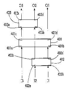
FIG. 4 is a block diagram that illustrates embodiments of a 3 x 3 MEM OXC
switch
;according to the present invention. Ac;c:ording to FIG. 4, a reduced number
of switches 401-403
~~an provide the interconnect needed to switch any of inputs I1-(3 to any of
outputs Ol-03. As
determined by equations (1) and (2), the 3 x 3 MEM OXC switch can include
three switches to
~arovide the needed 6 settings (3!) of the 3x3 MEM OXC switch.
Each of the switches 401-403 can operate as a 2 x 2 switch. In particular,
each switch
~I01-403 can have 2 inputs and 2 outputs, wherein optical radiation present at
the inputs can be
directed to the outputs by switching the optical radiation or by passing the
optical radiation
through ("pass-through"). For example, switch 402 can switch optical radiation
from an input
~I02a to an output 402d or can pass-through the optical radiation from the
input 402a to an output
~~02c. Similarly, the switch 402 can switch optical radiation from an input
402b to the output
~102c or pass-through the optical radiation from the input 402b to the output
402d.
The switches 401-403 can be coupled together to provide the overall function
of a 3 x 3
switch. Accordingly, optical energy can be switched from any input Il, I2,
and/or I3 to any
output O1, 02, and/or 03. In particular, the switch 402 can switch optical
energy from input I1
i;402b) and/or input I2 (402a) to the. switch 403 (via 402c) and/or to the
switch 401 (via 402d).
'The switch 401 can switch received optical energy (401a, 401b) to the switch
403 (via 401c)
and/or to the output O1 (via 401d). The switch 403 can switch received optical
energy from the
switch 401 (401a) and/or the switch 402 (401b) to the output 02 (via 403d)
and/or to the output
03 (via 403c). The dashed line through the switch 401 indicates that the
output 402c can be
coupled to the input 403b without being switched by the switch 401.
8
CA 02344112 2001-04-12
Doc. No.: CRO-13 CA Patent
Moreover, optical energy can be switched from a first input to a first output
without
Mocking the switching of optical energy from a second input to a second
output. For example,
;according to FIG. 4, switching optical energy from input I1 to output 02 does
not block (or
ypreclude) switching optical energy from input I2 to output O1 or to output
03.
FIG. 5 is a schematic diagram that illustrates embodiments of a 3 x 3 MEM OXC
switch
100 according to the present invention. According to FIG. 5, a 2 x 2 array
includes first and
;second columns and first and second rows that define first and second optical
paths 411, 412 in a
First direction 425 and third and four~.h optical paths 413, 414 in a second
direction 435. The
~~ptical paths are aligned with inputs and outputs of the MEM OXC switch.
In particular, input I1 is aligned with the first optical path 411, input I2
is aligned with the
Fourth optical path 414, and input 13 is aligned with the third optical path
413. Output O1 is
~~ligned with the first optical path 411, output 02 is aligned with the second
optical path 412, and
~~utput I3 is aligned with the third optical path 413.
As determined by, >Jquation (1), the 3 x 3 MEM OXC switch 400 includes the
three
switches or "switching nodes" 401-403 to provide the needed 6 settings (3!) of
the 3x3 MEM
OXC switch 400. The first, second, and third nodes 401-403 can selectively
switch optical
radiation from one optical path to another to propagate the optical radiation
from any input to
any output. For example, the first node 401 can switch optical radiation from
the first optical
path 411 to the third optical path 413 for output via the output I3 or the
first node 401 can pass
~:he optical radiation through to the input Il.
An optical transmission apparatus 405 can optically couple an output of the
second node
~I02 to an input of the third node 403 for output via the output 02 or 03. The
optical
~:ransmission apparatus 405 changes the direction of the propagation of
optical radiation received
from the second node 402 from the second direction 435 to the first direction
425 at the input to
l:he third node 403.
In preferred embodiments, the optical transmission apparatus 405 is non-
switching.
,Accordingly, the optical transmission apparatus 405 can be a fixed reflector,
a linear waveguide,
a curvilinear waveguide and/or other apparatus that can change the direction
of the propagation
of the optical radiation. However, a switching apparatus also may be used, but
need not be
moved between reflecting and non-reflecting positions.
9
CA 02344112 2001-04-12
Doc. No.: CRO-13 CA Patent
FIG. 6 is a plan view that illustrates embodiments of a 3 x 3 MEM OXC switch
500
.according to the present invention. According to FIG. 6, a 2 x 2 array of
reflectors 501-504 are
.arranged, as shown, in first and second columns and first and second rows to
define first and
~~econd optical paths 511, 512 in a first direction 525 and third and fourth
optical paths 513, 514
in a second direction 535. The optical paths are aligned with inputs and
outputs of the MEM
OXC switch 500.
In particular, input I1 is aligned with the first optical path 511, input I2
is aligned with the
fourth optical path 514, and input I3 is aligned with the third optical path
513. Output O1 is
;aligned with the first optical path 511, output 02 is aligned with the second
optical path 512, and
~~utput 03 is aligned with the third optical path. In a preferred embodiment,
at least one of the
unputs (here input I1) is located on a separate side of the MEM OXC 500 switch
from the other
inputs. In another embodiment, at least one of the outputs (here output 03) is
located on a
separate side of the MEM OXC switch 500 from the other outputs.
The first, second, and third reflectors 501-503 are moveable between a
reflecting position
and a non-reflecting position. The first, second, and third reflectors 501-503
are oriented 45
degrees relative to the optical paths and have reflective material on opposite
surfaces.
.Accordingly, the first, second, and third reflectors 501-503 can be used to
reflect or "switch"
~~ptical radiation from the inputs along; the optical paths to propagate the
optical radiation form
;any input to any output. The reflective material can be, for example, gold on
silicon or gold on
polysilicon. Other reflective materials may be used.
IFIG. 7 is a plan view that illustrates non-orthogonal embodiments of a 3 x 3
MEM OXC switch
according to the present invention. It will be understood that the present
invention can be
embodied in switches that use reflectors that have non-orthogonal orientations
with respect to
each other, as shown, for example, in FIG. 7.
FIG. 8 is a table that illustrates the (i switch settings for operations of a
3 x 3 MEM OXC switch
according to the present invention. According to FIG. 8, a first switch
setting optically couples
the input I1 to the output O1, the input I2 to the output 02, and the input I3
to the output 03. A
second switch setting optically couples the input I1 to the output O1, the
input I2 to the output
03, and the input I3 to the output 02. A third switch setting optically
couples the input I1 to the
output 02, the input I2 to the output O1, and the input I3 to the output 03. A
fourth switch
CA 02344112 2001-04-12
Doc. No.: CRO-13 CA Patent
setting optically couples the input I1 to the output 03, the input I2 to the
output 02, and the input
I3 to the output O1. A fifth switch setting optically couples the input I1 to
the output 02, the
input I2 to the output 3, and the input I3 to the output O1. A sixth switch
setting optically
~~ouples the input I1 to the output 3, the; input I2 to the output O1, and the
input I3 to the output
~02. Accordingly, the six switch settings of FIG. 8 allow any of the inputs to
be optically
~~oupled to any of the outputs.
FIGS. 9A-F is a series of plan views that illustrate embodiments of moveable
reflector 601-605
positions for each of the six switch settings of FIG. 8 in a 3 x 3 MEM OXC
switch 700
according to the present invention. As shown in FIG. 8, a 2 x 2 array of
reflectors 701-704 are
arranged, in first and second columns .and first and second rows to define
first and second optical
paths 711, 712 in a first direction 72.'~ and third and fourth optical paths
713, 714 in a second
~~irection 735. The optical paths are aligned with inputs and outputs of the
MEM OXC switch
'700.
According to FIGS. 9A-9F, solid shading indicates that the corresponding
moveable
reflector 701-703 is in the reflecting position, no shading indicates that the
reflector is in the non-
reflecting position, and half-shading indicates that the reflector is fixed.
When a moveable
reflector is in the reflecting position, optical radiation incident along a
first optical path reflects
from the first optical path to a second optical path orthogonal to the first
optical path. In
~~ontrast, when a moveable reflector is in the non-reflecting position,
optical radiation incident
along the first optical path will "pass-through" and continue to propagate
along the first optical
path.
As shown in FIG. 9A, in a first setting, first, second, and third moveable
reflectors 701-
'703 are in the respective non-reflecting positions. Accordingly, optical
radiation received at the
input I1 "passes-through" to the output O1. Optical radiation received at the
input I2 "passes-
through" the second moveable reflector 702 and rei~lects from the fixed
reflector 704 to the
output 02, and optical radiation received at the input I3 "passes-through" to
the output 03.
.Accordingly, the first setting can provide for 3 of the possible functions
provided by the MEM
OXC switch 200. In other words, the same setting may used to switch input I1
to output O1 or to
switch input I2 to output 02 or to switch input I3 to output 03.
11
CA 02344112 2001-04-12
Doc. No.: CRO-13 CA Patent
In a second setting, (FIG. 9B;1 the third moveable reflector 703 is in the
reflecting
position and the first and second reflectors 701-702 are in the non-reflecting
position.
.Accordingly, optical radiation received at the input I1 "passes-through" to
the autput Ol.
Optical radiation received at the input 12 "passes-through" the second
moveable reflector 702 and
reflects from the fixed reflector 704 to the third moveable reflector 703
which reflects the optical
energy to the output 03. Optical radiation received at the input I3 "passes-
through" the first
moveable reflector 701 and reflects from the third moveable reflector 703 to
the output 02.
In a third setting, (FIG. 9C) the second moveable reflector 702 is in the
reflecting
position and the fist and third moveable reflectors 701, 703 are in the non-
reflecting position.
.Accordingly, optical radiation received at the input Il reflects from the
second moveable
reflector 702 and from the fixed reflector 704 and "passes-through" the third
moveable reflector
'103 to the output 02. Optical radiation received at the input I2 reflects
from the second
moveable reflector 702 and "passes-through" the first moveable reflector 701
to the output O1.
Optical radiation received at the input IL3 "passes-through" to the output 03.
In a fourth setting, (FIG. 9D ) the first, second, and third moveable
reflectors 701-703 are
in the reflecting positions. Accordingly, optical radiation received at the
input Il reflects from
the second moveable reflector 701 to the fixed reflector 704 to the third
moveable reileetor 703
to the output I3. Optical radiation received at the input I2 reflects from the
second moveable
reflector 702 to the first moveable reflector 701 to the third moveable
reflector 703 to the output
t~2. Optical radiation received at the input I3 rel7ects from the first
moveable reflector 701 to the
output O1.
In an alternative fourth setting, (FIG. 9D') the first moveable reflector 701
is in the
reflecting position and the second and third moveable reflectors 702, 703 are
in the non-
reflecting position. Accordingly, optical radiation received at the input I1
"passes through" the
second moveable reflector 702 and reflects from the first moveable reflector
701 and "passes
through" the third moveable reflector 703 to the output 03. Optical radiation
received at the
input I2 "passes through" the second moveable reflector 702 and reflects from
the fixed reflector
'704 and "passes through" the third moveable reflector 703 to the output 02.
Optical radiation
received at the input I3 reflects from the first moveable reflector 701 to the
output O1.
12
CA 02344112 2001-04-12
Doc. No.: CRO-13 CA Patent
The one of the alternative fourth settings may be chosen over the other based
on the
desired operation of the 4 x 4 MEM OXC switch. For example, one alternative
fourth setting
may be favored because it may provide fewer reflections in propagating the
optical radiation
from an input to an output or because the associated optical path is shorter.
In a fifth setting, (FIG. 9E) the first and second moveable reflectors 701,
702 are in the
reflecting position and the third moveable reflector 703 is in the non-
reflecting position.
,accordingly, optical radiation received at the input I1 reflects from the
second moveable
reflector 702 to the fixed reflector 704 and "passes through" the third
moveable reflector 703 to
the output 02. Optical radiation received at the input I2 reflects from the
second moveable
reflector 702 to the first moveable reflector 701 and "passes though" the
third moveable reflector
'703 and the output 03. Optical radiation received at the input I3 reflects
from the first moveable
reflector 701 to the output O1.
In an alternative fifth setting, (FIG. 9E') the first and third moveable
reflectors 701, 703
are in the reflecting position and the second moveable reflector 702 is in the
non-reflecting
position. Accordingly, optical radiation received at the input I1 "passes
though" the second
moveable reflector 702 and reflects from the first moveable reflector 701 and
the third moveable
reflector 703 to the output 02. Optical radiation received at the input I2
"passes through" the
second moveable reflector 702 and retlects from the fixed reflector and the
third moveable
reflector 703 to the output 03. Optical radiation received at the input I3
reflects from the first
moveable reflector 701 to the output O 1.
In a sixth setting, (FIG. 9F) the second and third moveable reflectors 702,
703 are in the
reflecting position and the first moveable reflector 701 is in the non-
reflecting position.
~~ccordingly, optical radiation received at the input I1 reflects from the
second moveable
reflector 702 and the fixed reflector 704 and the third moveable reflector 703
to the output 03.
Optical radiation received at the input I2 reflects from the second moveable
reflector 702 and
"passes through" the first moveable reflector 701 to the output Ol. Optical
radiation received at
the input I3 "passes-through" the fig°st moveable retlector 701 and
reflects from the third
moveable reflector 703 to the output 02.
According to another aspect of the present invention, (NZ-N)/2 nodes can be
utilized to
create an N x N MEM OXC switch. :fn particular, the (Nz-N)/2 switching nodes
can be located
13
CA 02344112 2001-04-12
Doc. No.: CRO-13 CA Patent
~~n one side of a diagonal of the N x N array. One or more optical
transmission apparatus' are
located at the internal array positions along the diagonal. Accordingly, N x N
OXC switches
according to the present invention may include more moveable reflectors than
determined by
Equation (1). For example, a 4 x 4 MEM OXC switch according to the present
invention can use
5 moveable reflectors and 2 fixed reflector. An 8 x 8 MEM OXC switch may be
created using
28 moveable reflectors. In contrast. using Equation (1), these switches may
include fewer
movable reflectors.
FIG. 10 is a block diagram that illustrates embodiments of a 4 x 4 MEM OXC
switch
according to the present invention. According to FIG. 10, switches 801-805 can
provide the
interconnect needed to switch any of inputs Il-I4 to any of outputs O1-04. As
determined by
equations (1) and (2), the 4 x 4 ME:M OXC switch can include five switches to
provide the
needed 24 settings (4!) of the 4x4 MEM OXC switch.
In particular, each of the switches 801-805 can operate as a 2 x 2 switch. For
example,
switch 802 can switch optical energy from an input 802a to an output 802c
and/or an output
802d. Similarly, the switch 802 can switch optical energy from an input 802b
to the output 802c
~~nd/or the output 802d.
The switches 801-80S can be, coupled together to provide the overall function
of a 4 x 4
switch. Accordingly, optical energy can be switched from any input I1, I2, I3
and/or I4 to any
output O1, 02, 03 and/or 04. In particular, the switch 802 can switch optical
energy from the
input I2 (802b) and/or input I3 (802a) to the switch 804 (via 802c) and/or to
the switch 801 (via
802d). The switch 804 can switch optical energy from the switch 802 (via 804a)
and/or input I1
I;via 804b) to the switch 805 (via 804c) and/or to the switch 803 (via 804d).
The switch 801 can switch received optical energy (801a, 801b) to the switch
805 (via
801c) and/or to the switch 803 (via 801d). The switch 803 can switch received
optical energy
from the switch 801 (via 803a) and/or the switch 804 (via 803b) to the output
02 (via 803c)
and/or to the output O1 (via 803d). The switch 805 can switch received optical
energy from the
switch 801 (via 805a) and/or the switch 804 (via 805b) to the output 04 (via
805c) and/or to the
output 03 (via 805d).
The dashed line through the switch 804 indicates that the output 802d can be
coupled to
the input 801b without being switched by the switch 801. The dashed line
through the switch
14
CA 02344112 2001-04-12
lDoc. No.: CRO-13 CA Patent
801 indicates that the output 804c can be coupled to the input 805b without
being switched by
~.he switch 801.
FIG. 11 is a schematic diagram that illustrates embodiments of a 4 x 4 MEM OXC
switch 800 according to the present invention. According to FIG. 11, a 3 x 3
array includes first,
second, and third columns and first, second, and rows columns to define first,
second, and third
optical paths 811-813 in a first direction 825 and fourth, fifth, and sixth
optical paths 814-816 in
;a second direction 835. The optical paths are aligned with inputs and outputs
of the 4 x 4 MEM
~~XC switch 800.
In particular, input I1 is aligned with the second optical path 812, input I2
is aligned with
the first optical path 811, input I3 is aligned with the sixth optical path
816, and input I4 is
,aligned with the fifth optical path 815. Output O1 is aligned with the second
optical path 812,
~~utput 02 is aligned with the fourth optical path 814, output I3 is aligned
with the third optical
~~ath 813, and output I4 is aligned with the fifth optical path 815.
First through fifth nodes 801-805 can selectively switch optical radiation
from one optical
~aath to another to propagate the optical radiation from any input to any
output. For example, the
second node 802 can switch optical radiation from the first optical path 811
to the sixth optical
~~ath 816 for transmission to the fourth node 804 or can pass the optical
radiation through to the
First node 801.
A first optical transmission apparatus 806 can selectively optically couple an
output of
the fourth node 804 to an input of the fifth node 805 for output via the
output I3 or I4. The
~~ptical transmission apparatus 806 changes the direction of the propagation
of the optical
radiation received from the fourth node 804 from the second direction 835 to
the first direction
825 at the input to the fifth node 805.
A second optical transmission apparatus 807 can optically couple an output of
the first
node 801 to an input of the third node 803 for output via the output O1 or 02.
The optical
transmission apparatus 807 changes the direction of the propagation of optical
radiation received
~~rom the first node 801 from the first direction 825 to the second direction
835 at the input to the
third node 803.
The first and second optical transmission apparatus 806, 807 are not switched.
Accordingly, the first and second optical transmission apparatus 806, 807 can
be fixed reflectors,
CA 02344112 2001-04-12
Doc. No.: CRO-13 CA Patent
linear waveguides, curvilinear waveguides or other apparatus that can change
the direction of the
propagation of the optical radiation.
FIG. 12 is a plan view that illustrates embodiments of a 4 x 4 MEM OXC switch
900
.according to the present invention. According to FIG. 12, an array of first
through seventh
reflectors 901-907 are arranged, as shown, in first-third columns and first-
third rows to define
first, second, and third optical paths 911-913 in a first direction 925 and
fourth, fifth, and sixth
~~ptical paths 914-916 in a second direction 935. The optical paths are
aligned with inputs and
outputs of the MEM OXC switch 900.
In particular, input I1 is aligned with the second optical path 912, input I2
is aligned with
the first optical path 911, input I3 is aligned with the sixth optical path
916, and input I4 is
aligned with the fifth optical path 915'. Output O1 is aligned with the second
optical path 912,
output 02 is aligned with the fourth optical path 914, output 03 is aligned
with the third optical
path 913, and output 04 is aligned with the fifth optical path 915. In a
preferred embodiment, at
least one of the inputs is located on a sE;parate side of the MEM OXC switch
900 from the other
inputs. In another embodiment, at least one of the outputs is located on a
separate side of the
1VIEM OXC switch 900 from the other outputs.
The first through fifth reflectors 901-905 are moveable between a reflecting
position and
a non-reflecting position. The first through fifth moveable reflectors 901-905
are oriented 45
degrees relative to the optical paths a.nd have reflective material on
opposite surfaces thereof.
'Che sixth and seventh reflectors 906, 907 are fixed. Accordingly, the first
through fifth reflectors
!~01-905 can be used to reflect or "switch" optical radiation from the inputs
along the optical
paths therein to propagate the optical radiation from any input to any output.
The reflective
material can be, for example, gold on silicon or gold on polysilicon. Other
reflective materials
may be used.
FIG. 13 is a table that illustrates 24 switch settings for operations of a 4 x
4 MEM OXC
;witch according to the present invention. FIG. 14A-Y' is a series of plan
views that illustrate
embodiments of first through fifth moveable rel7ectors 901-905 in reflecting
and non-reflecting
positions for each of the 24 switch settings of FIG. 13 according to the
present invention. A
detailed explanation of each of FIGS. 14A-14Y' need not be provided because
the reflectors can
be positioned as shown in FIGs 14A-14Y' to provide the 24 settings needed.
16
CA 02344112 2001-04-12
Doc. No.: CRO-13 CA Patent
FIG. 15 is a schematic diagram that illustrates another embodiment of a 4 x 4
MEM
OXC switch including 5 switching nodes and first and second optical
transmission apparatus
according to the present invention. FIG. 16 is a plan view that illustrates
another embodiment of
a 4 x 4 MEM OXC switch including 5 moveable reflectors and 2 fixed reflectors
according to the
present invention.
FIG. 17 is a schematic diagram that illustrates another embodiment of a 4 x 4
MEM
OXC switch 1400 including 6 switching nodes and first and second optical
transmission
;apparatus according to the present invention. According to FIG. 17, a 3 x 3
array includes first,
:second, and third rows and first, secemd, and third columns that define
first, second. and third
optical paths 1411-1413 in a first direction 1425 and fourth, fifth, and sixth
optical paths 1414-
1416 in a second direction 1435. The optical paths are aligned with inputs and
outputs of the 4 x
<1 MEM OXC switch 1400.
In particular, input I1 is aligned with the first optical path 1411, input I2
is aligned with
i:he sixth optical path 1416, input I~ is aligned with the fifth optical path
1415, and input I4 is
.aligned with the fourth optical path 1414. Output Ol is aligned with the
first optical path 1411,
~~utput 02 is aligned with the second optical path 1412, output 03 is aligned
with the third
optical path 1413, and output 04 is aligned with the fourth optical path 1414.
First through sixth nodes 1401-1406 can selectively switch optical radiation
from one
~~ptical path to another to propagate the optical radiation from any input to
any output. For
~°xample, the fifth node 1405 can switch optical radiation from the
fifth optical path 1415 to the
;second optical path 1412 for transmission to the fourth node 1404 or can pass
the optical
radiation through to the sixth node 1406.
A first optical transmission apparatus 1407 can optically couple an output of
the third
node 1403 to an input of the fifth node 1405. The first optical transmission
apparatus 1407
~~hanges the direction of the propagation of optical radiation received from
the third node 1403
From the second direction 1435 to the first direction 1425 at the input to the
fifth node 1405.
A second optical transmission apparatus 1408 can optically couple an output of
the fifth
code 1405 to an input of the sixth rode 1406 for output via the output 03 or
04. The second
~~ptical transmission apparatus 1408 changes the direction of the propagation
of optical radiation
17
CA 02344112 2001-04-12
Doc. No.: CRO-13 CA Patent
received from the fifth node 1405 from the second direction 1435 to the first
direction 1425 at
uhe input to the sixth node 1406.
In FIGS. 15 and 16, the number of switching nodes/moveable reflectors can be
~~etermined by application of Equation (1). In particular the 4 x 4 OXC
switches of FIGS. 15 and
16 can include 5 switching nodes/rnoveable reflectors. In contrast to FIG. 11,
the moveable
reflectors of FIG. 16 may be oriented in different directions.
The first and second optical transmission apparatus 1407,1408 are not
switched.
Accordingly, the first and second optical transmission apparatus 1407, 1408
can be fixed
reflectors, linear waveguides, curvilinear waveguides or other apparatus that
can change the
direction of the propagation of the optical radiation.
As described above, (NZ - N)/2 switching nodes can be utilized to create the
embodiments illustrated by FIG. 17. 1~or example, in the 4 x 4 OXC switch 1400
shown in FIG.
17, (NZ - N)/2 (or nodes 1401-1406) can be located on one side of a diagonal
of a 4 x 4 array
where the interenal array positions of the 4 x 4 array are populated by first
and second optical
transmission apparatus.
According to the present invention, a number of reflectors used to provide the
functionality of an N x N MEM OXC switch can be reduced. In particular, the
reduced number
of reflectors can be expressed as: ceiling [ln(N!)/ln(2)]. Reducing the number
of reflectors used
in an N x N MEM OXC switch may allow for N x N switches that use fewer
actuators than
~~onventional N x N switches. Also, fewer reflectors and actuators may be
formed on a smaller
substrate area, allowing a reduction in the footprint of the N x N switch
according to the present
invention.
In the drawings and specification, there have been disclosed typical preferred
embodiments of the invention and, although specific terms are employed, they
are used in a
,generic and descriptive sense only and not for purposes of limitation, the
scope of the invention
being set forth in the following claims.
18