Note: Descriptions are shown in the official language in which they were submitted.
CA 02344487 2001-03-14
WO 00/20899 PCT/US99/21139
- 1 -
T _hni _a1 Fi 1 d
The present invention relates generally to the technical
field of fiber optics, and, more particularly, to free-space,
reflective NxN fiber optic switches.
gaclc~~-ound Art
A dramatic increase in telecommunications during recent
years, which may be attributed largely to increasing Internet
communications, has required rapid introduction and commercial
adoption of innovations in fiber optic telephonic communication
systems. For example, recently fiber optic telecommunication
systems have been introduced and are being installed for
transmitting digital telecommunications concurrently on 4, 16,
32, 64 or 128 different wavelengths of light that propagate along
a single optical fiber. While multi-wavelength fiber optic
telecommunications dramatically increases the bandwidth of a
single optical fiber, that bandwidth increase is available only
at both ends of the optical fiber, e.g. between two cities. When
light transmitted into one end of the optical fiber arrives at
the other end of the optical fiber, there presently does not
exist a flexible, modular, compact, NxN ffiber optic switch which
permits automatically forwarding light received at one end of the
optical fiber onto a selected one of several different optical
fibers which will carry the light onto yet other destinations.
Historically, when telecommunications were transmitted by
electrical signals via pairs copper wires, at one time a human
being called a telephone operator sat at a manually operated
switchboard and physically connected an incoming telephone call,
received on one pair of copper wires, that were attached to a
plug, to another pair of copper wires, that were attached to a
socket, to complete the telephone circuit. The telephone
operator's task of manually interconnecting pairs of wires from
two (2) telephones to establish the telephone circuit was first
replaced by an electro-mechanical device, called a crossbar
switch, which automated the operator's manual task in response
CA 02344487 2001-03-14
WO 00/20899 PCT/US99/21139
- 2 -
to telephone dialing signals. During the past forty years, the
electro-mechanical crossbar switch for electrical telecommunica-
tions has been replaced by electronic switching systems.
Presently, switches for fiber optic telephonic communica
tions exist which perform functions for fiber optic telephonic
communications analogous to or the same as the crossbar switch
and electronic switching systems perform for electrical telephon
ic communications. However, the presently available fiber optic
switches are far from ideal. That is, existing fiber optic
telecommunications technology lacks a switch that performs the
same function for optical telecommunications as that performed
by electronic switching systems for large numbers of optical
f fibers .
One approach used in providing a 256x256 switch for fiber
optic telecommunications first converts light received from a
incoming optical fiber into an electrical signal, then transmits
the electrical signal through an electronic switching network.
The output signal from that electronic switching network is then
used to generate a second beam of light that then passes into an
output optical fiber. As those familiar with electronics and
optical fiber telecommunications recognize, the preceding
approach for providing a 256x256 fiber optic switch is physically
very large, requires electrical circuits which process extremely
high-speed electronic signals, and is very expensive.
Attempting to avoid complex electronic circuits and
conversions between light and electronic signals, various
proposals exist for assembling a fiber optic switch that directly
couples a beam of light from one optical fiber into another
optical fiber. One early attempt to provide a fiber optic
switch, analogous to the electrical crossbar switch, mimics with
machinery the actions of a telephone operator only with optical
fibers rather than for pairs of copper wires. United States
Patent No. 4,886,335 entitled "Optical Fiber Switch System" that
issued December 12, 1989, includes a conveyor that moves ferrules
attached to ends of optical fibers. The conveyer moves the
ferrule to a selected adapter and plugs the ferrule into a cou-
pler/decoupler included in the adapter. After the ferrule is
plugged into the coupler/decoupler, light passes between the
CA 02344487 2001-03-14
WO 00/20899 PCT/US99/21139
- 3 -
optical fiber carried in the ferrule and an optical fiber secured
in the adapter.
United States Patent no. 5,864,463 entitled "Miniature 1xN
Electromechanical Optical Switch And Variable Attenuator" which
issued January 26, 1999, ("the '463 patent") describes another
mechanical system for selectively coupling light between one
optical fiber and one of a number of optical f fibers . This patent
discloses selectively coupling light between one optical fiber
and a selected optical fiber by mechanically moving an end of one
optical fiber along a linear array of ends of the other optical
fibers. The 1xN switch uses a mechanical actuator to coarsely
align the end of the one optical fiber to a selected one of the
other optical fibers within 10 ~,m. The 1xN switch, using light
reflected back into the moving optical fiber from the immediately
adjacent end of the selected optical fiber, then more precisely
aligns the end of the input optical fiber to the output optical
fiber. United States Patent no. 5,699,463 entitled "Mechanical
Fiber Optic Switch" that issued December 16, 1997, also aligns
an end of one optical fiber to one of several other optical
fibers assembled as a linear array, but interposes a lens between
ends of the two optical fibers.
United States Patent No. 5,524,153 entitled "Optical Fiber
Switching System And Method Of Using Same" that issued June 4,
1996, ("the '153 patent") disposes two (2) optically opposed
groups of optical fiber switching units adjacent to each other.
Each switching unit is capable of aligning any one of its optical
fibers with any one of the optical fibers of the optically
opposed group of switching units. Within the switching unit, an
end of each optical fiber is positioned adjacent to a beamforming
lens, and is received by a two-axis piezoelectric bender. The
two-axis piezoelectric bender is capable of bending the fiber so
light emitted from the fiber points at a specific optical fiber
in the optically opposed group of switching units. Pulsed light
generated by radiation emitting devices ("REDs") associated with
each optical fiber pass from the fiber to the selected optical
fiber in the opposing group. The pulsed light from the RED
received by the selected optical fiber in the opposing group is
processed to provide a signal that is fed back to the piezoelec-
CA 02344487 2003-09-09
- 4 -
tric bender for pointing light from the optical fiber directly at the
selected optical fiber.
Rather than mechanically effecting alignment of a beam of light
from one optical fiber to another optical fiber either by translating
or by bending one or both optical fibers, optical switches have been
proposed that employ micromachined moving mirror arrays to
selectively couple light emitted from an input optical fiber to an
output optical fiber. Papers presented at OFC/IOOC '99, February 21
- 26, 1999, Lin et al, Free-Space Micromachined Optical
Crossconnects: Routes to Enhanced Port-Count and Reduced Loss,
describe elements that could be used to fabricate a three (3) stage
fully non-blocking fiber optic switch, depicted graphically in FIG.
1. This fiber optic switch employs moving mirror arrays in which
each polysilicon mirror can selectively reflect light at a 90° angle.
In this proposed fiber optic switch, rows of relatively small 32 x
64 optical switching arrays 52ai (i = 1, 2 w 32) and 52bk (k = 1, 2
32) receive light from or transmit light to thirty-two (32) input
or output optical fibers 54an and 54bn. Thirty-two groups of sixty
four (64) optical fibers 56a1, m and 56b1, m carry light between each
of the 32 x 64 optical switching arrays 52ai and 52bk and one of
sixty-four 32 x 32 optical switching arrays 58~ (j - l, 2 ~~~ 64).
The complexity of the fiber optic switch illustrated in FIG. 1
is readily apparent. For example, a 1024 x 1024 fiber optic switch
assembled in accordance with that proposal requires 4096 individual
optical fibers for interconnecting between the 32 x 64 optical
switching arrays 52ai and 52bk and the 32 x 32 optical switching
arrays 58~. Moreover, the 32 x 64 optical switching arrays 52ai and
52bk and 32 x 32 optical switching arrays 58~ require a total of
196,608 micromachined mirrors.
The polysilicon mirrors proposed for the fiber optic switch
illustrated in FIG. 1 are curved rather than optically flat.
Furthermore, while those mirrors possess adequate thermal dissipation
for switching a single 0.3 mW wavelength of light and perhaps even
a few such wavelengths, they are incapable of switching even ten (10)
or twenty (20) such wavelengths. However, as described above fiber
optic telecommunications systems are already transmitting many more
CA 02344487 2003-09-09
- 5 -
than twenty (20) wavelengths over a single optical fiber and if not
already, will soon be transmitting hundreds of wavelengths. If
instead of a single wavelength of light one optical fiber carries 300
different wavelengths of light each having a power of 0.3 mW, then
100 mW of power impinges upon the polysilicon mirror proposed for
this fiber optic switch. If the polysilicon mirror reflects 98.5%
of that light, the mirror must absorb substantially all of the
remainder, i.e. 1.5 mW of power. Absorption of 1.5 mW of power would
likely heat the thermally non-conductive polysilicon mirror to
unacceptable temperatures which would further degrade mirror
flatness.
Disclosure of Invention
The present invention provides a fiber optic switch capable of
concurrently coupling incoming beams of light carried on more than
1,000 individual optical fibers to more than 1,000 outgoing optical
fibers.
The present invention seeks to provide a simpler fiber optic
switch that is capable of switching among a large number of incoming
and outgoing beams of light carried on optical fibers.
Another aspect of the present invention seeks to provide an
efficient fiber optic switch that is capable of switching among a
large number of incoming and outgoing beams of light carried on
optical fibers.
Still further the present invention seeks to provide a fiber
optic switch which has low cross-talk between communication channels.
Further still the present invention seeks to provide a fiber
optic switch which has low cross-talk between communication channels
during switching thereof.
Yet further the present invention seels to provide a highly
reliable fiber optic switch.
Still further the present invention seeks to provide a fiber
optic switch that does not exhibit dispersion.
Further the present invention seeks to provide a fiber optic
switch that is not polarization dependent.
Another aspect of the present invention seeks to provide a fiber
optic switch that is fully transparent.
CA 02344487 2003-09-09
- 6 -
Moreover, the present invention seeks to provide a fiber optic
switch that does not limit the bitrate of fiber optic
telecommunications passing through the switch.
Briefly the present invention is a fiber optic switch that
includes a fiber optic switching module that receives and fixes ends
of optical fibers. In addition to receiving and fixing ends of
optical fibers, the fiber optic switching module includes a plurality
of reflective light beam deflectors which may be selected as pairs
to be oriented responsive to drive signals for coupling a beam of
light between a pair of optical fibers fixed in the fiber optic
switching module. The fiber optic switching module also produces
orientation signals from each light beam deflector which indicate its
orientation.
In addition to the fiber optic switch module, the fiber optic
switch also includes at least one portcard that supplies the drive
signals to the fiber optic switching module for orienting at least
one light beam deflector included therein. Furthermore, the portcard
also receives the orientation signals produced by that light beam
deflector together with coordinates that specify an orientation for
the light beam deflector. The portcard compares the received
coordinates with the orientation signals received from the light beam
deflector and adjusts the drive signals supplied to the fiber optic
switching module to reduce any difference between the received
coordinates and the orientation signals.
In a preferred embodiment, the fiber optic switching module
of the fiber optic switch includes a first and a second group of
optical fiber receptacles which are separated from each other at
opposite ends of a free space optical path. Each of these groups
of optical fiber receptacles are adapted for receiving and fixing
ends of optical fibers. The fiber optic switching module
includes lenses juxtaposed with ends of optical fibers fixed
respectively at the first and second groups and disposed along
the optical path between the groups. Each of these lenses are
respectively disposed with respect to an end of an associated
optical fiber of the first or second group so that beams of
light as may be emitted from the end of the optical fiber pass
through the immediately adjacent lens to propagate as a
CA 02344487 2001-03-14
WO 00/20899 PC'T/US99/21139
quasi-collimated beams through the optical path from the lens
toward the second or first group of optical fiber receptacles.
The preferred embodiment of the fiber optic switch also
includes a first and a second sets of reflective light beam
deflectors that are both disposed along the optical path between
the groups of optical fiber receptacles. Each of the sets of
light beam deflectors are associated with one of the groups of
optical fiber receptacles and have a number of light beam deflec-
tors that equals the optical fibers in the group with which it
is associated. Each of the light beam deflectors in the first
or the second set is:
1. associated with one of the optical fibers in the
associated group of optical fiber receptacles;
2. along the optical path so the quasi-collimated beam of
light as may be emitted from the lens associated with
the optical fiber impinges upon the light beam deflec
tor to be reflected therefrom through the optical
path; and
3. energizable by drive signals supplied to the fiber
optic switching module to be oriented for reflecting
the quasi-collimated beam of light as may be emitted
from the associated optical fiber to also reflect off
a selected one of the light beam deflectors in the
second or the first set.
In this way a pair of light beam deflectors, one light beam
deflector of the pair belonging to the first set and one
belonging to the second set, may be selected and oriented by the
drive signals supplied to them to couple a quasi-collimated beam
of light propagating through the optical path from the end of one
optical fiber fixed in an optical fiber receptacle either of the
first or of the second group to reflect sequentially off the pair
of energized light beam deflectors into a selected one of the
optical fiber receptacles so as to enter an optical fiber as may
be ffixed at the second or at the first group of optical fiber
receptacles.
In a preferred embodiment the portcard of the fiber optic
switch includes a driver circuit for supplying the drive signals
to the fiber optic switching module for orienting at least one
CA 02344487 2001-03-14
WO 00/20899 PCT/US99/21139
- g -
light beam deflector included in the fiber optic switching
module. The portcard also includes a dual axis servo that
receives coordinates which specify an orientation for the light
beam deflector, and also receives the orientation signals
produced by that light beam def lector . The portcard compares the
received coordinates with the orientation signals received from
the light beam deflector and adjusts the drive signals supplied
to the fiber optic switching module to reduce any difference
between the received coordinates and the orientation signals.
These and other features, objects and advantages will be
understood or apparent to those of ordinary skill in the art from
the following detailed description of the preferred embodiment
as illustrated in the various drawing figures.
R i f D a inion df Drawings
FIG. 1 is a block diagram illustrating a proposed, prior art
three (3) stage fully non-blocking fiber optic switch;
FIG. 2 is a plan view ray tracing diagram illustrating
propagation of light beams through a trapezoidally-shaped free
space, convergent beam NxN reflective switching module in
accordance with the present invention;
FIG. 3 is a plan or elevational schematic diagram illustrat-
ing a single beam of light as may propagate between sides A and
B of the trapezoidally-shaped free space, convergent beam NxN
reflective switching module depicted in FIG. 2 in accordance with
the present invention;
FIG. 4a is a perspective view ray tracing diagram illustrat-
ing propagation of light beams through an alternative embodiment,
rectangularly-shaped free space, convergent beam NxN reflective
switching module in accordance with the present invention;
FIG. 4b is plan view ray tracing diagram illustrating
propagation of convergent light beams through the rectangularly-
shaped reflective switching module illustrated in FIG. 4a in
accordance with the present invention;
FIG. 5 is a plan view ray tracing diagram illustrating
propagation of light beams through an alternative embodiment,
polygonally-shaped free space, convergent beam NxN reflective
switching module in accordance with the present invention;
CA 02344487 2001-03-14
WO 00/20899 PCT/US99/21139
_ g _
FIG. 6 is a plan~view ray tracing diagram illustrating
propagation of light beams through a trapezoidally-shaped free
space, convergent beam reflective switching module in accordance
with the present invention that permits coupling a beam of light
between any arbitrarily chosen pair of optical fibers;
FIG. 7 is a plan view ray tracing diagram illustrating
propagation of light beams through an alternative trapezoidally-
shaped free space, convergent beam NxN reflective switching
module in accordance with the present invention which is more
compact than the NxN reflective switching module depicted in FIG.
5;
FIG. 8a is an elevational view illustrating a preferred,
cylindrically shaped micro-lens adapted for use in the NxN
reflective switching module;
FIG. 8b is an elevational view illustrating a micro-lens
adapted for use in the NxN reflective switching module that
permits closer spacing between lenses and fibers;
FIG. 9 is a partially cross-sectioned elevational view
illustrating a block included both in the side A and in side B
of the NxN reflective switching module depicted in FIG. 7 that
receives tapered optical fiber collimator assemblies;
FIG. 10 is a partially cross-sectioned plan view illustrat-
ing the block depicted in FIG. 9 that receives tapered optical
fiber collimator assemblies;
FIG. 11 is a partially cross-sectioned elevational view
illustrating a micro-lens adapted for use in the NxN reflective
switching module for concurrently switching light carried by a
duplex pair of optical fibers;
FIG. 12 is an elevational view illustrating a preferred type
of silicon wafer substrate used in fabricating torsional
scanners;
FIG. 13 is a plan view illustrating a 2D electrostatically
energized torsional scanner particularly adapted for use in
reflective switching modules such as those illustrated in FIGS.
2, 4a-4b, 5, 6 and 7;
FIG. 14 is an enlarged plan view illustrating a torsional
flexure hinge used in the torsional scanner taken along the line
14-14 in FIG. 13;
CA 02344487 2001-03-14
WO 00/20899 PCTNS99/21139
- 10 -
FIG. 15 is a schematic cross-sectional elevational view
illustrating a torsional scanner disposed above an insulating
substrate having electrodes deposited thereon with a beam of
light reflecting off a mirror surface located on the backside of
a device layer;
FIGs. 15a and 15b are alternative plan views of the
electrodes and a portion of the insulating substrate taken along
the line 15a/15b-15a/15b in FIG. 15.
FIG. 16a is an elevational view illustrating a strip of
torsional scanners adapted for use in reflective switching
modules such as those illustrated in FIGS. 2, 4a-4b, 5, 6 and 7;
FIG. 16b is a cross-sectional plan view taken along the line
16b-16b in FIG. l6a illustrating overlapping immediately adjacent
strips of torsional scanners to reduce the horizontal distance
between immediately adjacent strips;
FIG. 16c is an elevational view illustrating a preferred
strip of torsional scanners adapted for use in reflective
switching modules such as those illustrated in FIGS. 2, 4a-4b,
5, 6 and 7;
FIG. 16d is a cross-sectional plan view illustrating the
preferred strip of torsional scanners taken along the line
16d-16d in FIG. 16c;
FIG. 16e is across-sectional plan view taken along the line
16d-16d in FIG. 16a illustrating juxtaposition of the strips of
torsional scanners depicted in FIG. 16c;
FIG. 17a is a plan view illustrating vertically offset
strips of torsional scanners which permits a denser arrangement
of optical fibers in reflective switching modules such as those
illustrated in FIGs. 2, 4a-4b, 5, 6 and 7;
FIG. 17b is a plan view illustrating an even denser packing
of offset rows or columns of torsional scanners that may be
employed if all the torsional scanners are fabricated as a single
monolithic array rather than in strips;
FIG. 18a is a plan view illustrating an alternative
embodiment of the torsional scanner in which the outer torsional
flexure hinges are oriented diagonally with respect to the
scanner's outer frame;
CA 02344487 2001-03-14
WO 00/20899 PCT/US99/21139
- 11 -
FIG. 18b is a plan view illustrating an array of torsional
scanner of the type illustrated in FIG. 18a;
FIG. 19a is a plan view illustrating an alternative
embodiment of the torsional scanner in which the inner torsional
flexure hinges are oriented along a diagonal of the scanner's
non-square mirror plate;
FIG. 19b is a plan view illustrating an alternative
embodiment of the torsional scanner depicted in FIG. 19a in which
both pairs of torsional flexure hinges are suitably oriented with
respect to crystallographic directions of silicon to permit
fabrication of torsion sensors therein that have optimum
characteristics;
FIG. 20a is an elevational view illustrating a dense
arrangement of the torsional scanner illustrated in FIG. 18a
adapted for inclusion in reflective switching modules such as
those illustrated in FIGS. 2, 4a-4b, 5, 6 and 7;
FIG. 20b is an elevational view illustrating a dense
arrangement of the torsional scanner illustrated in FIG. 19a
adapted for inclusion in reflective switching modules such as
those illustrated in FIGS. 2, 4a-4b, 5, 6 and 7;
FIG. 21 is a schematic cross-sectional elevational view
illustrating an alternative embodiment strip of torsional
scanners fastened to a substrate which also carries a mirror
strip thereby permitting an arrangement in which collimator
lenses and ends of optical fibers are positioned close to mirrcr
surfaces on the torsional scanners;
FIGS. 22a is a front elevational view of a strip of
torsional scanners flip-chip bonded to a substrate;
FIGs. 22b is a cross-sectioned, side elevational view of the
strip of torsional scanners flip-chip bonded to the substrate
taken along the line 22b-22b in FIG. 22a;
FIGS. 22c is a top view of the strip of torsional scanners
that is flip-chip bonded to the substrate taken along the line
22c-22c in FIG. 22a;
FIGs. 22d is a cross-sectioned, side elevational views of
the strip of torsional scanners flip-chip bonded to a silicon
substrate having vias formed therethrough;
CA 02344487 2001-03-14
WO 00/20899 PCT/US99/21139
- 12 -
FIG. 23 is a ray tracing diagram illustrating scattering of
light from portions of a torsional scanner that surrounds the
mirror surface thereof;
FIG. 24 is a system level block diagram illustrating
reflective switching modules such as those illustrated in FIGs.
2, 4a-4b, 5, 6 and 7;
FIG. 25 is a perspective drawing illustrating a modular
fiber optic switch in accordance with the present invention;
FIG. 26 is a overall block diagram for modular fiber optic
switch depicted in FIG. 25 including a portcard and the reflec-
tive switching module;
FIG. 26a is a diagram illustrating one embodiment of photo
detectors that may be used in an optical alignment servo for
precisely orienting a pair of mirrors included in the reflective
switching module;
FIG. 26b is a diagram illustrating a compound photo-detector
that may be used in an optical alignment servo for precisely
orienting a pair of mirrors included in the reflective switching
module;
FIG. 27a is a block diagram illustrating a servo system
which ensures precise alignment of mirrors included in a
reflective switching module included in the modular fiber optic
switch depicted in FIG. 25, such as one of the reflective
switching modules illustrated in FIGs. 2, 4a-4b, 5, 6 and 7;
FIG. 27b is a block diagram illustrating one channel, either
x-axis or y-axis, of a dual axis servo included in the servo
system depicted in FIG. 27a;
FIG. 28a is a partially cross-sectioned elevational view
illustrating an alternative embodiment double plate structure for
receiving and fixing an array of optical fibers;
FIG. 28b is an elevational view illustrating a profile for
one type of hole that may be formed through one of the plates
taken along the line 28b-28b in FIG. 28a;
FIG. 28c is an elevational view illustrating an array of XY
micro-stages formed in one of the plates taken along the line
28c-28c in FIG. 28a;
CA 02344487 2001-03-14
WO 00/20899 PCT/US99/21139
- 13 -
FIG. 29a is an elevational view illustrating an XY micro-
stage of a type included array taken along the line 29a-298 in
FIG. 28c;
FIGS. 29b and 29c are elevational views illustrating a
portion of alternative embodiment XY micro-stages taken along the
line 29b/29c-29b/29c in FIG. 29a;
FIG. 30a is a partially cross-sectioned view illustrating
a lens micromachined from a silicon substrate that can be
electrostatically activated to move along the lens' longitudinal
axis;
FIG. 30b is an elevational view illustrating the silicon
micromachined lens taken along the line Sob-30b in FIG. 30a;
FIG. 30c is a partially cross-sectioned view illustrating
a lens micromachined from a silicon substrate, similar to the
lens illustrated in FIG. 30a, that can be electro-magnetically
activated to move along the lens' longitudinal axis; and
FIG. 31, is an elevational view that illustrates coupling
beams of light from a routing wavelength demultiplexer directly
into one of the reflective switching modules illustrated in FIGs.
2, 4a-4b, 5, 6 and 7.
RPCt Mod for arming Ont the Tnvention
Free Space,
Convergent Beam,
Double Bounce,
Reflective S~ritchiny Module
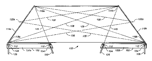
FIG. 2 depicts ray tracings for light beams propagating
through a trape2oidally-shaped, convergent beam, double bounce
NxN reflective switching module in accordance with the present
invention that is referred to by the general reference character
100. The NxN reflective switching module 100 includes sides 102a
and 102b which are spaced apart from each other at opposite ends
of a C-shaped free space optical path. Although as described
below other geometrical relationships for the sides 102a and 102b
may occur for other configurations of the NxN reflective
switching module 100, for the embodiment of the NxN reflective
switching module 100 illustrated in FIG. 2 having the C-shaped
free space optical path the sides 102a and 102b are preferably
CA 02344487 2001-03-14
WO 00/20899 PCT/US99121139
- 14 -
coplanar. Both side 102a and side 102b are adapted to receive
and fix ends 104 of N optical fibers 106, for example one-
thousand one-hundred fifty-two (1152) optical fibers 106. The
N optical fibers 106 are arranged in a rectangular array with
thirty-six (36) columns, each of which contains thirty-two (32)
optical fibers 106. A lens 112 is disposed immediately adjacent
to the ends 104 of each of the optical fibers 106 along the
optical path between sides 102a and 102b. Each of the lenses 112
are disposed with respect to the end 104 of the optical f fiber 106
with which it is associated to produce from light, which may be
emitted from the end 104 of the associated optical fiber 106, a
quasi-collimated beam that propagates along the optical path
between sides 102a and 102b.
FIG. 3 graphically illustrates a single beam of light 108
from a single optical fiber 106 as may propagate between sides
102a and 102b, or conversely. For wavelengths of light conven
tionally used in single mode fiber optic telecommunications, the
lens 112 is a micro-lens which typically has a focal length of
2.0 to 12.0 mm. Such a lens 112 produces a quasi-collimated beam
preferably having a diameter of approximately 1.5 mm which
propagates along a five-hundred (500) to nine-hundred (900) mm
long path between the sides lo2a and 102b. Since the NxN
reflective switching module 100 preferably uses the maximum relay
length of the lens 112, the end 104 of each optical fiber 106 is
positioned at the focal length of the lens 112 plus the Raleigh
range of the beam of light 108 emitted from the optical ffiber
106. Consequently, if the end 104 of the optical fiber 106 is
displaced a few microns along the axis of the lens 112, that
produces a negligible effect on the direction along which the
maximum relay length quasi-collimated beam propagates between the
sides 102a and 102b. Typically the exit angle of the maximum
relay length quasi-collimated beam from the lens 112 will be a
fraction of one milliradian, i.e. 0.001 radian. As will be
described in greater detail below, any possible misalignment of
the maximum relay length quasi-collimated beam due to misalign-
ment between the end 104 of the optical fiber 106 and the lens
112 can be easily accommodated by providing sufficiently large
surfaces from which the beam reflects.
CA 02344487 2003-09-09
- 15 -
After passing through the associated lens 112, a beam of light
108 emitted from the end 104 of each optical fiber 106 reflects first
off a mirror surface 116a or 116b, indicated by dashed lines in FIG.
3, that is associated with a particular lens 112 and optical fiber
106 pair. The mirror surfaces 116, described in greater detail
below, are preferably provided by two-dimensional ("2D") torsional
scanners of a type similar to those described in United States Patent
No 5,629,790 ("the 1790 patent"); which may be referred to for
further details. The N x N reflective switching module 100 includes
two sets 118a and 118b of mirror surfaces 116 respectively disposed
between the lenses 112 along the optical path between the sides 102a
and 102b. Each set 118a or 118b includes a number of individual,
independent mirror surfaces 116, each of which is supported by a pair
of gimbals that permits each mirror surface 116 to rotate about two
non-parallel axes. The number of mirror surfaces 116 equals the
number, N, of optical fibers 106 and lenses 112 at the nearest side
102a or 102b. After reflecting off the mirror surface 116a or 116b,
the beam of light 108, propagating between sets 118a and 118b in FIG.
2, then reflects off a selected one (1) of the mirror surface 116b
or 116a further along the C-shaped optical path between the sides
102a and 102b, through one of the lenses 112 at the distant side 102b
or 102a and into the optical fiber 106 associated with that
particular lens 112.
FIGS. 4a - 4b depict ray tracings for light beams propagating
through an alternative embodiment, rectangularly-shaped,
convergent N x N reflective switching module 100. The
rectangularly-shaped configuration of the N x N reflective switching
module 100 illustrated in FIGS. 4a - 4b employs a horizontally
elongated Z-shaped free space optical path. While in the
illustration of this FIG. the distances between the side 102a and the
curved set 118a, the curved set 118a and the curved set 118b, the
curved set 118b and the side 102b are substantially equal, those
skilled in the art will recognize that these distances need not be
equal. Moreover, those skilled in the art will recognize that the
sets 118a and 118b may be curved to provide either one dimensional
("1D") or 2D convergence. Thus, for the configuration of the N x N
reflective switching module 100 depicted in FIGS. 4a - 4b the
CA 02344487 2001-03-14
WO 00/20899 PCT/US99/21139
- 16 -
curved set 118a may be advantageously moved nearer to the side
102a and the curved set 118b moved nearer to the side 102b. Such
a shortening of the distances between the sides 102a and 102b and
the curved sets 118a and 118b correspondingly lengthens the
distance between the curved set 118a and curved set 118b which
produces a parallelogram-shaped NxN reflective switching module
100. FIG. 5 depicts ray tracings for light beams propagating
through an alternative embodiment, polygonally-shaped NxN
reflective switching module 100. The polygonally-shaped
configuration of the NxN reflective switching module 100
illustrated in FIG. 5 also produces a Z-shaped free space optical
path.
FIG. 6 depicts a trapezoidally-shaped reflective switching
module 100 that consist of only one half of the NxN reflective
switching module 100 depicted in FIG. 1, i. e. either the left
half thereof or the right half thereof. The reflective switching
module 100 depicted in FIG. 6 fundamentally differs from that
depicted in FIG. 1 only by including a mirror 120 disposed at the
middle of the optical path between sides 102a and 102b. While
for equivalent sides 102a the reflective switching module 100
depicted in FIG. 6 can couple light selectively between only one-
half as many optical fibers 106 as the NxN reflective switching
module 100 illustrated in FIG. 1, the reflective switching module
100 depicted in FIG. 6 can couple light between any arbitrarily
chosen pair of those optical fibers 106. FIG. 7 depicts another
trapezoidally shaped NxN reflective switching module 100 which
also employs a mirror 120 for folding the optical path of the NxN
reflective switching module 100 depicted in FIG. 5. Folding the
optical path into a W-shape provides a more compact reflective
switching module 100 than the NxN reflective switching module 100
depicted in FIG. 1.
Considering the beam of light 108 depicted schematically in
FIG. 3, solely from the perspective of optical design, the
various different embodiments of the reflective switching module
100 described above and illustrated in FIGs. 2, 4a, 4b, 5, 6, and
7 differ principally in the location of the mirror surfaces 116a
and 116b along the beam of light 108, and in the folding of the
optical path. For example, in the embodiment of the NxN
CA 02344487 2001-03-14
' ~"~~~1«V~ ~s~ 11 ~g
DOCKET NO. 2149
. 3.
- 17 -
reflective switching module 100 illustrated in FIGs. 4a-4b the
mirror surfaces 116a and 116b are located approximately one-third
(3) of the path length between the sides 102a and 102b from the
nearest lenses 112. Conversely for other configurations of the
reflective switching module 100 such as those illustrated in
FIGS. 2, 5, 6, and 7 the mirror surfaces 116a and 116b are
immediately adjacent to the respective sides 102a and 102b.
However, those skilled in the art of optical design will readily
understand that differences among the various configurations,
particularly locations for the mirror surfaces 116a and 116b with
respect to the lenses 112 and the ends 104 of the optical fibers
106, influence or affect other more detailed aspects of the
optical design.
Those skilled in the art of optical design will also
understand that conceptually there exist an unlimited number of
other possible geometrical arrangements and optical path shapes
in addition to those illustrated in FIGs. 2, 4a, 4b, 5, 6 and 7
L..i for placing the ends 104 of the optical fibers 106 respectively
at one or more the sides 102a and 102b, the associated lenses 112
and the mirror surfaces 116a and 116b. With regard to such
alternative geometrical arrangements for the free space optical
path of the reflective switching module 100, a preference for one
arrangement in comparison with other possible arrangements
usually involves issues related to suitability for a particular
optical switching application, size, ease of fabrication,
relaxing mechanical tolerances for assembly of the reflective
switching module 100, reliability, cost, etc. Specifically, the
trapezoidally-shaped, convergent beam NxN reflective switching
module 100 with the W-shaped free space optical path illustrated
in FIG. 7 is presently preferred because:
1. it fits within a standard twenty-three (23) inch wide
telecommunications rack;
2. mechanical tolerances are acceptable;
3. long effective relay length for the beams of light
108; and
4. runs for electrical cables and optical cables are well
separated.
..~_.._ _. _
CA 02344487 2001-03-14
J r
DOCKET NO. 2149
r
- 18 -
As described above, the beam of light 108 produced by the
lens 112 from light emitted from the end 104 of the associated
optical fiber 106 first impinges upon the associated mirror
surface 116 of one of the torsional scanners included in the sets
118a and 118b. As described in greater detail below, for the
configuration of the NxN reflective switching module 100 depicted
in FIG. 7, the mirror surfaces 116 are preferably provided by
thirty-six (36) linear strips of thirty-two (32) torsional
scanners. Preferably, all thirty-two (32) mirror surfaces 116
in each strip are substantially coplanar. As an example, within
each strip immediately adjacent mirror surfaces 116 may be spaced
3.2 mm apart, and the immediately adjacent columns of mirror
surfaces 116 are preferably spaced 3.2 mm apart with respect to
the beams of light 108 impinging thereon from the immediately
adjacent sides 102a and 102b.
Also for all the various configurations of the NxN reflec-
tive switching module 100, the ends 104 of the optical fibers
106, the lenses 112, and the mirror surfaces 116 of un-energized
torsional scanners are preferably oriented so all of the beams
of light 108 produced by light emitted from optical fibers 106
having their ends 104 at the side 102a converge at a point 122b
that is located behind the set 118b of mirror surfaces 116.
Correspondingly, the beams of light 108 emitted from optical
fibers 106 having their ends 104 at the side 102b converge at a
point 122a that is located behind the set 118a of mirror surfaces
116. Horizontally the convergence point 122 is established by
considering mirror surfaces 116 at opposite sides of the sets
w 118a and 118b. The point 122 lies at the intersection of two
lines that respectively bisect angles having their vertices at
those two mirror surface 116 and sides which extend from the
respective mirror surfaces 116 through mirror surfaces 116 at
opposite ends of the other set 118b or 118a. The point 122 is
located vertically one-half the height of the sets 118a and 118b.
The geometrical arrangement of the ends 104 of the optical fibers
106, the lenses 112, and the mirror surfaces 116 which produces
the preceding convergence provides equal clockwise and counter-
clockwise rotation angles and minimal rotation angles for mirror
surfaces 116 for each of the sets 118a and 118b that require the
,~~ir~'~u~i3 ~;-<''~.~
CA 02344487 2001-03-14
WO 00/20899 PCT/US99/21139
- 19 -
greatest movement in reflecting a beam of light 108 from one
mirror surface 116 in the set 118a or 118b to any of the mirror
surfaces 116 in the other set 118b or 118a. If in the configura-
tion for the NxN reflective switching module 10o depicted in FIG.
7 a pair of mirror surfaces 116a and 116b are separated six-
hundred and fifty (650) mm along the beam of light 108, then the
maximum angular rotation of the mirror surfaces 116 is approxi-
mately 3.9° clockwise and counter-clockwise.
Although individual pairs of optical fibers 106 and lenses
112 could be inserted into grooves to assemble the sides 102a and
102b which yield the convergence of the beams of light 108
described in the preceding paragraph, for maximum density of
lenses 112 and optical fibers 106 a monolithic block is prefera
bly used that has holes appropriately pre-drilled therein. Each
pre-drilled hole receives one of the lenses 112 and a conven
tional optical fiber ferrule secured about the end 104 of one
optical fiber 106. The compound angles required to align the
optical fiber 106 and the lens 112 for 2D convergence of the
beams of light 108 are provided by suitably orienting the holes
drilled into the block.
FIG. 8a depicts a preferred, cylindrically shaped micro-lens
112 fabricated with its focal point at, or as close as possible
to, a face 138 of the lens 112. As those skilled in the art of
fiber optics will understand, the optical fiber 106 emits the
beam of light 108 at an angle with respect to a center line of
the optical fiber 106 because the end 104 is polished at an angle
to eliminate reflections back from the end 104. Because the end
104 is angled, the axis of the beam of light 108 emitted from the
end 104 diverges from the longitudinal axis of the optical fiber
106. To align the beam of light 108 with a longitudinal axis 144
of the lens 112, the face 138 of the lens 112 is angled to center
the beam of light 108 within the lens 112. With the focal point
of the lens 122 at the face 138 as described above, the end 104
of the optical fiber 106 is positioned one Raleigh range of the
beam of light 108, e.g. 50-60 microns, from the face 138. The
diameter of a cylindrical surface 136 of the lens 112 is made
sufficiently large to contain the diverging beam of light 108
CA 02344487 2001-03-14
WO 00/20899 PCT/US99/21139
- 20 -
before it exits the lens 112 through a convex surface 142 as the
quasi-collimated beam of light 108.
This configuration for the lens 112 and the end 104 of the
optical fiber 106 centers the beam of light 108 about the
longitudinal axis 144 of the lens 112 and the optical fiber
collimator assembly 134 at the convex surface 142 of the lens
112, with the quasi-collimated beam of light 108 oriented
essentially parallel to the longitudinal axis 144. Usual
manufacturing tolerances for the lens 112 described above produce
acceptable deviations in exit angle and offset of the beam of
light 108 from the longitudinal axis 144 of the lens 112. For
example, if the lens 112 is fabricated from BK7 optical glass and
the end 104 of the optical fiber 106 angles at 8 ° , then the angle
of the beam of light 108 within the lens 112 is 6.78°, and the
lateral offset from the longitudinal axis 144 is less than 50
microns both at the face 138 and also 140 mm from the face 138.
Such a well centered beam of light 108 permits reducing the
diameter of the surface 136 thus allowing the lenses 112 to be
placed closer to each other. This lens 112 is preferably made
from Gradium material marketed by LightPath Technologies, Inc.
FIG. 8b depicts an alternative embodiment "champagne cork"
shaped micro-lens 112 which advantageously permits spacing lenses
112 and optical fibers 106 closer together at the sides 102a and
102b. The lens 112 includes a smaller diameter surface 132 which
a comically-shaped optical fiber collimator assembly 134
illustrated in FIG. 9 receives. The larger diameter surface 136
of the lens 112 protrudes out of the optical fiber collimator
assembly 134. The champagne cork shaped embodiment of the micro
lens 112 may be fabricated by grinding down a portion of the lens
112 illustrated in FIG. 8a.
As illustrated in FIG. 9, in addition to receiving one of
either the cylindrically shaped lens depicted in FIG. 8a or the
champagne cork shaped micro-lens 112 depicted in FIG. 8b, each
optical fiber collimator assembly 134 also provides a receptacle
that receives a conventional fiber optic ferrule 146 secured
about the end 104 of the optical fiber 106. A convergence block
152, one of which is respectively disposed at both sides 102a and
102b of the reflective switching module 100, is pierced by a
CA 02344487 2001-03-14
WO 00/20899 PCT/US99/21139
- 21 -
plurality of conically shaped holes 154 as illustrated in FIG.
that equal in number to the number N of optical fibers 106.
Convergence of the beams of light 108 as described above is
effected by the alignment of the optical fiber collimator
5 assemblies 134 upon insertion into the holes 154. The optical
fiber collimator assemblies 134 and holes 154 are preferably
formed from the same material with identically shaped, mating,
conical surfaces that taper at an angle of a few degrees.
Configured in this way, when all optical fiber collimator
10 assemblies 134 carrying the optical fibers 106 are fully seated
into their mating holes 154, the optical fiber collimator
assemblies 134 becomes fixed in the convergence block 152 and
hermetically seal the interior of the ref lective switching module
100 through which the quasi-collimated beams of light 108
propagate.
The convergence block 152 may be simply machined out a
single piece of metal such as stainless steel, or from a ceramic
material, etc. Alternatively, the convergence block 152 may be
made out of Kovar, 42 ~ nickel-iron alloys, titanium (Ti),
tungsten (W) or molybdenum (Mo) suitably plated for corrosion
resistance. These materials all have coefficients of expansion
which approximately match that of the lenses 112 and minimize
birefringent effects that may take place as lenses 112 are heated
or cooled in their operating environment.
In addition to the preceding preferred way of providing
convergence by suitably orienting the optical fibers 106 and the
lenses 112 at each of the sides 102a and 102b, either 1D or 2D
convergence may also be obtained in other ways. For example, the
configuration of the optical fibers 106 and the lenses 112 could
provide some of the convergence which the arrangement of the
mirror surfaces 116 upon which the beams of light 108 first
impinge could provide the remainder of the convergence. For
example the mirror surfaces 116 in each column could be arranged
along a cylindrical surface. Alternatively, the optical fibers
106 arid the lenses 112 might be arranged to provide none of the
convergence, i.e. beams of light 108 propagate parallel from the
sides 102a and 102b to the first mirror surfaces 116, with the
mirror surfaces 116 being arranged to provide all of the
CA 02344487 2001-03-14
WO 00/20899 PCTNS99/21139
- 22 -
convergence as illustrated in FIGS. 4a-4b. For example the
mirror surfaces 116 in each column could be arranged along a
spherical surface. Moreover, the optical fibers 106, lenses 112,
and sets 118a and 118b of mirror surfaces 116 may be arranged to
provide either 1D or 2D convergence either behind the sets 118a
and 118b or at the sets 118a and 118b. With regard to the
various alternative ways of arranging convergence of the beams
of light 108, selecting one way in comparison with other possible
ways usually involves issues related to ease of fabrication,
relaxing mechanical tolerances for assembly of the reflective
switching module 100, reliability, cost, etc.
The preceding convergence criterion not only affects the
optical design of the reflective switching module 100, that
criteria also interacts with reliability considerations. If each
optical fiber 106 of a reflective switching module 100 capable
of switching among 1152 optical fibers 106 carries a beam of
light 108 having a total power of 100 mW, the cumulative power
of all beams of light 108 passing through the reflective
switching module 100 at any instant is in excess of 100 watts.
However, assuming that, on average, equal numbers of the beams
of light 108 propagate in opposite directions between the sides
102a and 102b, then at any instant, on average, each set 118a or
118b of mirror surfaces 116 reflects beams of light 108 carrying
slightly more than 50 watts of power. From a worst-case analysis
perspective, at any instant beams of light 108 carrying at least
50 watts of power impinge either on one or the other of the set
118a or 118b of mirror surfaces 116. If electrical power
supplied to the reflective switching module 100 for orienting the
mirror surfaces 116 were to fail, then within a short time, e.g.
milliseconds, at least 50 watts of power and perhaps more than
100 watts of power becomes directed at the convergence point.
This amount of power would soon destroy the one or the few of the
mirror surfaces 116 included in the set 118a or 118b upon which
all of the beams of light 108 concentrate. To prevent such an
catastrophe from occurring, the sets 118a and 118b both omit any
mirror surfaces 116 from their centers where the beams of light
108 will converge if electrical power to the ref lective switching
module 100 should fail. To detect such a failure, the reflective
CA 02344487 2001-03-14
WO 00/20899 PCT/US99/21139
- 23 -
switching module 100 may include a photo-detector behind this
hole in the mirror surfaces 116.
In most telecommunication installations, optical fibers are
generally matched as a duplex pair in which one fiber carries
communications in one direction while the other fiber of the pair
carries communications in the opposite direction. Connectors
adapted for coupling light between two duplex pairs of optical
fibers which secure the two optical fibers of a pair in a single
ferrule are presently available. Because both optical fibers of
a duplex pair are switched concurrently, and because the
reflective switching module 100 can couple light in either
direction between a pair of optical fibers 106 one of which is
respectively located at side 102a and the other of which is
located at side 102b, suitably adapting the lenses 112 for use
with duplex pairs of optical fibers 106 permits using a single
pair of mirror surfaces 116a and 116b for switching light carried
in opposite directions respectively in the two optical fibers 106
of the duplex pair.
FIG. 11 depicts a lens 112 adapted for use in the reflective
switching module 100 for concurrently switching light carried by
a duplex pair of optical fibers 106a and 106b. As illustrated
in FIG. 11, the duplex optical fiber ferrule 146 carries the
duplex pair of optical fibers 106a and 106b. The ends 104a and
104b of the optical fibers 106a and 106b and the faces 138a and
138b of the lens 112 are all polished at an angle. The angles
of the faces 138a and 138b are formed to compensate for the off-
axis position of the optical fibers 106a and 106b so beams of
light 108a and 108b impinging upon faces 138a and 138b from the
optical fibers 106a and 106b are formed into quasi-collimated
beams which exit the convex surface 142 parallel to but slightly
offset from the longitudinal axis 144, and propagate in that way
through the reflective switching module 100. Both of the beams
of light 108a and 108b impinge upon the same pair of mirror
surfaces 116a and 116b which are made large enough to simulta-
neously reflect both beams of light 108a and 108b. When the two
quasi-collimated beams of light 108a and 108b impinge upon
another identically configured lens 112 and duplex pair of
optical fibers 106 at the opposite side 102a or 102b of the
CA 02344487 2003-09-09
- 24 -
reflective switching module 100, the lens 112 located there couples
the beams of light 108a and 108b into the respective optical fibers
106 of the duplex pair.
Torsional Mirror Configuration
As described above, the mirror surfaces 116a and 116b of the
sets 118a and 118b are preferably provided by electrostatically
energized 2D torsional scanners of a type described in the '790
patent. United States Patent No. 6,044,705 issued April 4, 2000 and
Published Patent Cooperation Treaty ("PCT") Patent Application
International Publication Number: WO 98/44571, both of which may be
referred to for further details, provide additional more detailed
information regarding the preferred 2D torsional scanner. Hinges
which permit the mirror surfaces 116 to rotate about two (2) non-
parallel axes preferably include torsion sensors of a type disclosed
in United States Patent No~5,648,618 ("the '618 patent") which also
may be referred to for further details . The torsion sensors included
in the hinges measure rotation of a second frame or a plate, that has
been coated to provide the mirror surface 116, respectively with
respect to the first frame or with respect to the second frame.
As described in the patents and patent applications
identified above, torsional scanners are preferably fabricated
by micro-machining single crystal silicon using Simox, silicon-
on-insulator or bonded silicon wafer substrates. Such wafer
substrates are particularly preferred starting material for
torsional scanner fabrication because they permit easily
fabricating a very flat, stress-free membrane, possibly only a few
microns thick, which supports the mirror surfaces 116. As
illustrated in FIG. 12, a silicon-on-~,nsulator ("SOI") wafer 162
includes an electrically insulating silicon dioxide layer 164
that separates single crystal silicon layers 166 and 168.
Torsion bars and plates that carry the mirror surfaces 116 of
torsional scanners are formed in the thinner device silicon layer
166 while other portions of torsional scanners are formed ty
backside etching in the thicker handle silicon layer 168. As is
well known to those skilled in the art of micro-machining, the
device silicon layer 166 has a frontside 169 furthest from the
CA 02344487 2001-03-14
WO 00/20899 PCTNS99/21139
- 25 -
handle silicon layer 168 and a backside 170 at the silicon
dioxide layer 164. The intermediate silicon dioxide layer 164
provides a perfect etch stop for etching the wafer 162 from its
backside, and yields torsion bars and plates having uniform
thickness.
FIG. 13 depicts a single electrostatically energized 2D
torsional torsional scanner 172 adapted for providing the mirror
surfaces 116 for the reflective switching module 100. The
torsional scanner 172 includes an outer reference frame 174 to
which are coupled a diametrically opposed pair of outer torsional
flexure hinges 176. The torsional flexure hinges 176 support an
inner moving frame 178 for rotation about an axis established by
the torsional flexure hinges 176. A diametrically opposed pair
of inner torsional flexure hinges 182 couple a central plate 184
to the inner moving frame 178 for rotation about an axis
established by the torsional flexure hinges 182. The axes of
rotation established respectively by the torsional flexure hinges
176 and by the torsional flexure hinges 182 are non-parallel,
preferably perpendicular.
It is important to note that the plate 184 of the torsional
scanner 172 is rectangularly shaped with the longer side being
approximately 1.4 times wider than the height of the plate 184.
The plate 184 included in the reflective switching module 100 has
a rectangular shape because the beam of light 108 impinges
obliquely at an angle of 45° on the mirror surface 116 carried
by the plate 184. Consequently, for reflection of the beam of
light 108 from the mirror surface 116 the rectangularly shaped
plate 184 becomes effectively square. The plate 184 is prefera-
bly 2.5 mm x 1.9 mm, and is typically between 5 and 15 microns
thick as are the inner moving frame 178, the torsianal flexure
hinges 176 and 182. The torsional flexure hinges 176 and 182 are
between 200 and 400 microns long, and between 10 and 40 microns
wide. The resonance frequencies on both axes are on the order
of 400 to 800 Hz which permits switching a beam of light 108
between two optical fibers 106 in approximately 1 to 5 millisec-
onds. Both the frontside 169 and the backside 170 of the plate
184 are coated in perfect stress balance with identical metallic
adhesion layers, preferably 10.0 to 100.0 A° of titanium (Ti) or
CA 02344487 2003-09-09
- 26 -
zirconium (Zr) which underlie a 500 to 800 A° thick metallic
reflective layer of gold (Au).
The torsional flexure hinges 176 and 182, which are illustrated
in greater detail in FIG. 14, provide various advantages in
comparison with a conventional unfolded torsion bar. A United States
Patent No. 6,392,220 and published Patent Cooperation Treaty ("PCT"~
International Patent Application WO 00/13210, which are both entitled
"Micromachined Members Coupled for Relative Rotation by Torsional
Flexure Hinges", which were both filed September 2, 1999, by Timothy
G. Slater and Armand P. Neukermans and which may be referred to for
further details, describe in greater detail various advantages
provided by the torsional flexure hinges 176 and 182. Most
significant for the reflective switching module 100, the torsional
flexure hinges 176 and 182 are more compact than a conventional
unfolded torsion bar having an equivalent torsional spring constant.
Consequently, use of the torsional flexure hinges 176 and 182 instead
of a conventional unfolded torsion bar permits making much smaller
torsional scanners 172 that can be packed more closely together which
correspondingly increases the number of optical fibers 106 that may
be accommodated at the sides 102a and 102b of the reflective
switching module 100.
Each torsional scanner 172 included in the reflective switching
module 100 includes a pair of torsion sensors 192a and 192b, of a
type disclosed in the ' 618 patent . The torsion sensors 192a and 192b
measure orientation of the supported member, i.e. the plate 184 or
the inner moving frame 178, with respect to the supporting member,
i.e. the inner moving frame 178 or the outer reference frame 174, at
a theoretical resolution of approximately 1.0 micro-radians. In
accordance with the description in the '618 patent, when the
torsional scanner 172 is operating in the ref lective switching module
100 an electrical current flows in series through the two torsion
sensors 192a and 192b between a pair of sensor-current pads 194a and
194b. Accordingly, the torsional scanner 172 includes a meandering
metal conductor 196 that is bonded to the frontside 169 of the
device silicon layer 166. Starting at the sensor-current pad
CA 02344487 2001-03-14
DOCKET X10. 214 9
~~.~~ ~Q~21139
f~~ ; ~ ~~~~r 200
- 26.1 -
194a, the meandering metal conductor 196 crosses the immediately
adjacent torsional flexure hinge 176 from the outer reference
_.~ ,., .~
._..__.
CA 02344487 2001-03-14
WO 00/20899 PCT/US99/21139
- 27 -
frame 174 onto the inner moving frame 178 to reach the X-axis
torsion sensor 192b that is located in the lower torsional
flexure hinge 182. From the X-axis torsion sensor 192b the
meandering metal conductor 196 continues onto a reflective,
stress balanced metal coating, that is applied to both sides of
the plate 184 to provide the mirror surface 116, and across the
plate 184 and the upper torsional flexure hinge 182 back onto the
inner moving frame 178. The meandering metal conductor 196 then
leads to the Y-axis torsion sensor 192a that is located in the
left hand torsional flexure hinge 176. From the Y-axis torsion
sensor 192a, the meandering metal conductor 196 then curves
around the outer reference frame 174 to the sensor-current pad
194b. Metal conductors, that are disposed on opposite sides of
the meandering metal conductor 196 across the right hand
torsional flexure hinge 176 and on the inner moving frame 178,
connect a pair of inner-hinge sensor-pads 198a and 198b to the
X-axis torsion sensor 192b. Similarly, metal conductors, one of
which is disposed along side the meandering metal conductor 196
on the outer reference frame 174 and the other with curves around
the opposite side of the torsional scanner 172 on the outer
reference frame 174, connect a pair of inner-hinge sensor-pads
202a and 202b to the Y-axis torsion sensor 192a. A pair of
grooves 204, cut only through the device silicon layer 166 on
opposite sides of the inner-hinge sensor-pads 198a and 198b,
increase electrical isolation between the sensor-current pad 194a
and the inner-hinge sensor-pads 198a and 198b and the
sensor-current pad 194b and the inner-hinge sensor-pads 202a and
202b.
Preferably, the backside 170 of the plate 184 provides the
mirror surface 116 because, as illustrated in FIG. 15, the
frontside 169 faces an insulating substrate 212 which carries
both electrodes 214 used in energizing rotation of the plate 184
and contacts for the sensor-current pads 194a and 194b, the
inner-hinge sensor-pads 198a and 198b and the inner-hinge
sensor-pads 202a and 202b not illustrated in FIG. 15. The plates
184 of each torsional scanner 172 are separated a distance, e.g.
from 40 to 150 microns, from the substrate 212 by spacers which
are also not depicted in FIG 15. The separation between the
CA 02344487 2001-03-14
!~'~ "~~ ~~~ ~'~9
DOCKET NO. 2119 ~~~~ - L ; ~~,Y 240
- 28 -
plate 184 and the substrate 212 depends upon how far edges of the
plate 184 move during rotation.
Note that for the reflective switching module 100, very thin
plates 184, only a few microns thick, are desirable and can be
fabricated using the device silicon layer 166 of the wafer 162.
In many instances the plate 184 and the tarsional flexure hinges
176 and 182 can be made of the same thickness as the. device
silicon layer 166. Alternatively, as illustrated in FIG. 15 the
torsional flexure hinges 182 may be thinned by etching. For
example, the torsional flexure hinges 182 may be 6 microns thick
while the plate 184 may be 10 microns thick. Analogously, the
plate 184 may be thinned to reduce its moment of inertia by
etching a cavity 216 into the plate 184 leaving reinforcing ribs
218 on the thinned plate 184.
A telecommunication system component such as the reflective
switching module 100 must exhibit high reliability. A plate 184
of the torsional scanner 172 that accidentally collides with the
electrode 214 should not stick to it, and should immediately
rotate to its specified orientation. Furthermore, such acciden-
tal collisions should not damage the torsional scanner 172, or
any circuitry connected to the torsional scanner 172. To
preclude stiction, as illustrated in FIG. 13 the periphery of the
plate 184 and of the inner moving frame 178 have rounded corners
that reduce the strength of the electrostatic field. Rounding
the periphery of the plate 184 also reduces its effective turning
radius which results from compound rotation of the plate 184
about the axes respectively established by both torsional flexure
hinges 176 and 182.
In addition to rounding the periphery of the plate 184 and
the inner moving frame 178, as illustrated in FIG. 15a locations
where the plate 184 may contact the electrodes 214 are overcoated
with electrical insulating material 219 such as polyimide.
Overcoating only those portions of the electrodes 214 which may
contact the plate 184 with the electrical insulating material 219
avoids charge stored on most of the electrodes 214. Analogously,
during fabrication of the torsional scanner 172 some of the
silicon dioxide layer 164 may be left at the periphery of the
plate 184 so the metallic reflective layer which provides the
R(~f~ND~D ~~i'
CA 02344487 2003-09-09
- 29 -
mirror surface 116 never contacts the electrode 214. Alternatively,
as illustrated in FIG. 15B holes 220 are formed through the metal of
the electrodes 214 in areas of possible contact.
During operation of the reflective switching module 100, the
torsional scanner 172 is at a ground electrical potential while
driving voltages are applied to the electrodes 214. To reduce
electrical discharge currents if the plate 184 contacts the
electrodes 214, large resistors (e.g. 1.0 MS2) may be connected in
series with the driving circuit for the electrodes 214. Ideally
these resistors should be located as close as practicable to the
electrodes 214 otherwise the conductor connecting between the
electrodes 214 and the resistors might pick up stray electric fields
that rotate the plate 184. . Therefore, one alternative is to overcoat
the electrodes 214 with a very high resistivity but slightly
conductive material in selected areas such as those illustrated in
FIG. 16a to provide a bleed path from the electrodes 214 for DC
charges. Furthermore, inputs of all amplifiers connected to
torsional scanners 172, such as those which receive orientation
signals from the torsion sensors 192a and 192b, should include diode
protection to prevent damage from an over-voltage condition due to
arcing or accidental contact between the plate 184 and the electrodes
214.
Several configurations exist that may be exploited
advantageously to increase the density of the mirror array, which is
usually the limiting factor on the density of optical fibers 106 at
the sides 102a and 102b. For several reasons, particularly the large
number of contacts that must be brought out for each torsional
scanner 172, the torsional scanners 172 are preferably arranged into
strips 222 as illustrated' in FIGS. 16a and 16b. Organizing the
~30 torsional scanners 172 into strips 222 increases their density above
that which might be achieved if arranged as a 2 dimensional array of
discrete torsional scanners 172. Each strip 222 includes a metal
support frame 224 to which the substrate 212 is fastened.
As explained in greater detail below, the strip 222 is flip
chip bonded to the substrate 212 so all electrical connections to the
strip 222 are made between the strip 222 and the substrate 212,
A flat polyimide backed multi-conductor ribbon cable 226
CA 02344487 2001-03-14
WO 00/20899 PCT/US99/21139
- 30 -
connects to the substrate 212 to exchange electrical signals
between the pads 194, 198 and 202 and the electrodes 224. Since
each support frame 224 may be an open frame possibly including
reinforcing ribs, the ribbon cable 226 can be freely bent and
guided away from the substrate 212.
FIG. 16b illustrates how, without obscuring the mirror
surfaces 116, the substrates 212 and the strips 222 may be
overlapped with the ribbon cable 226 serpentined along the
staircased substrates 212. Arranging the strips 222 in this way
reduces the horizontal distance between the mirror surfaces 116
of immediately adjacent strips 222 in relationship to the beams
of light 108. Since the beams of light 108 impinge upon the
mirror surfaces 116 at approximately 45°, the. apparent distance
between immediately adjacent strips 222 is further foreshortened
by a factor of approximately 1.4 which, as described above, is
why the plate 184 is preferably rectangularly shaped.
One disadvantage with the configuration of strips 222
illustrated in FIG. 16b is that the offset between immediately
adjacent strips 222 cannot be less than the thickness of the
torsional scanners 172 plus the substrate 212. Furthermore,
overlapping of immediately adjacent strips 222 and substrates 212
hinders removing a single defective strip 222 without disturbing
immediately adjacent strips 222.
FIGS. 16c and 26d illustrate a preferred embodiment for the
strips 222 and the support frames 224 in which electrical leads
228 that connect to the torsional scanners 172 are plated or
screened onto one face, around one edge, and onto the other face
of the substrate 212. With this configuration for the leads 228,
attachment of the ribbon cable 226 to the substrate 212 is
unhindered. Plating or screening the leads 228 onto the
substrate 212 and including some via holes through the substrate
212 permits the substrate 212 to be as narrow as the strip 222.
Narrowed to this extent, the combined strips 222, substrates 212
and support frames 224 may now be arranged as illustrated in FIG.
16e for both of the sets 118a and 118b. This permits the offset
between immediately adjacent strips 222 to be established as
required by the optics of the reflective switching module 100
rather than by packaging considerations. The optimum offset
CA 02344487 2001-03-14
WO 00/20899 PCT/US99/21139
- 31 -
between immediately adjacent strips 222 is approximately 0% to
10% of the distance between plates 184 in immediately adjacent
strips 222. The configuration of the substrate 212 illustrated
in FIG. 16d facilitates access to the substrate 212 and removal
of the strip 222 without disturbing adjacent support frames 224.
Note that if necessary the leads 228 may be brought out around
both edges of the substrate 212. This capability may be
exploited advantageously to separate leads 228 carrying high
voltage driving signals that are applied between the plate 184
and the electrodes 214 from leads 228 which carry signals from
the torsion sensors 192a and 192b.
Without reducing the size of the plate 184, as illustrated
in FIG. 17a the density of the optical fibers 106 at the sides
102a and 102b may be increased by offsetting the torsional
scanners 172 of immediately adjacent strips 222 vertically by
one-half the vertical distance between torsional scanners 172
within the strip 222. Due to the convergence criteria set forth
above for arranging the beams of light 108 within the reflective
switching module 100, offsetting the torsional scanners 172 in
immediately adjacent strips 222 effects a reorganization of the
holes 154 which receive the optical fiber collimator assemblies
134 from a quasi rectangular array into a quasi hexagonally close
packed array. While offsetting the torsional scanners 172 in
immediately adjacent strips 222 does not increase the density of
the torsional scanners 172, such an arrangement of the torsional
scanners 172 does increase the density of the optical fibers 106
at the sides 102a and 102b to the extent that the diameter,
either of lenses 112 or of optical fiber collimator assemblies
134, limits the spacing between immediately adjacent optical
fibers 106.
The density of torsional scanners 172 may be even further
increased by fabricating the torsional scanners 172 as completely
monolithic two dimensional arrays rather than as strips 222. As
illustrated in FIG. 17b, offsetting the torsional scanners 172
in immediately adjacent columns permits interdigitation of the
torsional flexure hinges 176 of torsional scanners 172 into an
empty space that occurs between torsional scanners 172 in
immediately adjacent columns or rows of the array. This
CA 02344487 2001-03-14
WO 00/20899 PCTNS99/21139
- 32 -
interdigitating of the torsional flexure hinges 176 provides a
shorter distance between centers of plates 184 of torsional
scanners 172 in adjacent columns or rows, and more closely
approximates a hexagonal close packing of the torsional scanners
172 and, correspondingly, of the optical fibers 106 at the sides
102a and 202b.
An alternative embodiment for strips 222 orients the
torsional flexure hinges 176 and 182 at 45° with respect to the
vertical and horizontal axes of the support frame 224. FIGs. 18a
and 18b illustrate a diagonal configuration for the torsional
flexure hinges 176 and 182 which more efficiently uses area on
the strips 222 than a configuration in which the torsional
flexure hinges 176 and 182 are oriented parallel and perpendicu-
lar to strips 222. Using a diagonal orientation for the
torsional flexure hinges 176 and 182 oriented at 45° with respect
to the outer reference frame 174, they can be longer without
increasing the area occupied by the torsional scanner 172. The
plate 184 is elongated in one direction to accommodate the 45°
impingement angle of the beam of light 108. Due to the
elliptical shape of the beam of light 108 as it impinges upon the
plate 184, corners of the beam of light 108 may be eliminated
resulting in an octagonally shaped plate 184, which conveniently
provides room for the outer reference frame 174. Sides of the
outer reference frame 174 are oriented in the <110> crystallo-
graphic direction of silicon for ease of fabrication. This
configuration for the torsional scanner 172 orients the torsion
sensors 192a and 192b along the <100> crystallographic direction
of silicon. Thus, a wafer 162 having a p-type device silicon
layer 166 or p-type implantation must be used in fabricating the
torsion sensors 192a and 192b. The <110> and <100> crystallo-
graphic directions of silicon may be interchanged with suitable
process changes.
Using the arrangement of the torsional scanner 172 illus
trated in FIG. 18b, 1.5 x 2 mm plates 184 may be spaced only 2.5
mm apart effectively increasing the density of mirror surfaces
116 by a factor of 1.4. When viewed at the approximate 45°
incident angle of the beams of light 108, the strips 222 slope
at 54°. In this configuration the strips 222 are oriented at
CA 02344487 2001-03-14
WO 00/20899 PCT/US99/21139
- 33 -
45° to the support frames 224. This orientation of the strips
222 is necessary if the mirror surfaces 116 are to fully
intercept the beams of light 108. The support frames 224 could
be oriented at 45° which permits all the strips 222 to be the
same length, thereby using area on wafers 162 more efficiently.
FIG. 19a illustrates yet another alternative embodiment of
the torsional scanner 172 which further reduces its size thereby
further shortening distances between immediately adjacent mirror
surfaces 116 in the reflective switching module 100. From the
l0 preceding description it is apparent that positioning the
torsional flexure hinges 176 and 182 at corners rather than sides
of the plate 184 advantageously reduces the size of the torsional
scanner 172. In FIG. 19a an elliptically-shaped curve 232
represents an outline of the beam of light 108 impinging on the
mirror surface 116 of the plate 184. Because the beam of light
108 does not impinge on the corners of the plate 184, the inner
torsional flexure hinges 182 may be rotated with respect to the
plate 184 to occupy unused corner space. As in the configuration
of the torsional scanner 172 illustrated in FIG. 18a, the outer
torsional flexure hinges 176 continues to occupy corners of the
outer reference frame 174.
Not only does placement of the torsional flexure hinges 182
at the corners of the plate 184 as illustrated in FIG. 19a reduce
the size of the torsional scanner 172, it also reduces compound-
ing of the angles when the plate 184 rotates simultaneously about
both axes. Compounding increases the distance through which
corners of the plate 184 move when the plate 184 simultaneously
rotates about axes established by both torsional flexure hinges
176 and 182. Compounding increases the separation required
between the plate 184 and the substrate 212 which correspondingly
increases the voltage that must be applied between the plate 184
and the electrodes 214 for equivalent performance in rotating the
plate 184. However, if the plate 184 has an aspect ratio that
is not square as will usually occur for plates 184 included in
the reflective switching module 100, then the torsion sensors
192a and 192b in torsional flexure hinges 176 and 182 depicted
in FIG. 19a are no longer oriented along orthogonal crystallo-
graphic directions, i.e. either <100> ar <110> directions, of
CA 02344487 2001-03-14
WO 00/20899 PCT/US99/21139
- 34 -
silicon. This is undesirable, since the torsion sensors 192a and
192b in the torsional flexure hinges 176 and 182 then respond
both to bending and torsion of the torsional flexure hinges 176
and 182.
Because the plate 184 depicted in FIG. 19a has an aspect
ratio of approximately 1.4:1, axes of rotation 236a and 236b
established by the torsional flexure hinges 176 and 182 intersect
at approximately 70.5°. However, reorienting the axes of
rotation 236a and 236b slightly until they intersect at 90°, as
illustrated in FIG. 19b, permits the torsional flexure hinges 176
and 182 to be oriented along a single crystallographic direction
of silicon, e.g. the <100> crystallographic orientation if the
outer reference frame 174 is aligned along the <110> crystallo-
graphic direction of silicon. Configured as illustrated in FIG.
19b, the torsional scanner 172 provides a significant amount of
space for the inner torsional flexure hinges 182 in the corners
of the plate 184 which reduces the size of the torsional scanner
172. Furthermore, the configuration of the torsional scanner 172
illustrated in FIG. 19b preserves the crystallographic orienta-
tion of the torsion sensors 192a and 192b while the compounding
effect, though not completely eliminated, is significantly
reduced. However, in the configuration of the torsional scanner
172 depicted in FIG. 19, the orthogonal axes of rotation
established by the torsional flexure hinges 176 and 182 are
oriented obliquely to the length and width of the plate 184.
Nevertheless, because only small angular rotations of the plate
184 occur during operation of the reflective switching module 100
the area of the plate 184 upon which the beam of light 108
impinges changes insignificantly when the plate 184 rotates.
Incorporating the torsional scanners 172 illustrated in
FIGS. 18a or 19a into one of the set 118a or 118b of mirror
surfaces 116 to maximize their respective advantages requires
rearranging the shape of the set 118a or 118b. A preferred
arrangement for strips 222' of torsional scanners 172 depicted
in FIG. 18a is illustrated in FIG. 20a. As described above and
depicted FIG. 20a, the strips 222' are mounted at a 45° angle
with respect to a horizontal base 242 of the reflective switching
module 100. In the illustration of FIG. 2oa, the support frames
CA 02344487 2001-03-14
WO 00/20899 PCT/US99/21139
- 35 -
224' carrying the strips 222' are also mounted at a 45° angle
with respect to the base 242. The two axes established by the
torsional flexure hinges 176 and 182 abaut which the plates 184
rotate are indicated by x and y axes 244 depicted in FIG. 20a.
The maximum rotation angles for plates 184 about axes established
by the torsional flexure hinges 176 and 182 allowed for identical
torsional scanners 172 at the other set 118b or 118a of mirror
surfaces 116 establishes a serrated rectangularly-shaped field
246 of addressable torsional scanners 172 in the addressed set
118a or 118b.
This optimum rectangularly-shaped f field 246 is truncated at
the corners and has sides that are approximately diagonal to the
strips 222'. For the arrangement illustrated in FIG. 20a, the
longest strip 222' must include at least 1.4 times more torsional
scanners 172 than that required for a rectangular array of the
torsional scanners 172 assembled from the strip 222 illustrated
in FIG. 16a. However, torsional scanners 172 may be omitted from
locations in the set 118a or 118b that cannot be addressed from
the other set 118b or 118a. Thus, only a few of the strips 222'
illustrated in FIG. 20a need be full length. Those strips 222'
that include only a few torsional scanners 172 might even be
eliminated entirely. For example by using 40 strips 222'
containing a maximum 44 torsional scanners 172, it is possible
to arrange as many as 1152 torsional scanners 172 in the set 118a
or 118b, with very small scan angles, and relatively small mirror
sizes. A different arrangement provides for 1132 torsional
scanners 172, which measure only 1.59 by 2.2 mm, and requires
deflection angles of 3.69° and 3.3°. The strips 222' of the
torsional scanners 172 are oriented at an average of 55° to the
optical fiber collimator assemblies 134. The arrangement
illustrated in FIG. 20a, though slightly more complex substan-
tially increases the density of the torsional scanners 172 and,
correspondingly, the optical fiber collimator assemblies 134, and
allows more scanners to be addressed for particular rotation
angles specified for the plates 184.
FIG. 20b illustrates an analogous re-arrangement at the sets
118a and 118b of torsional scanners 172 of the type depicted in
FIG. 19b. For this arrangement of the torsional scanners 172
CA 02344487 2001-03-14
WO 00/20899 PCT/US99/21139
- 36 -
depicted in FIG. 19b the strips 222" and the support frames 224"
are oriented vertically similar to the illustration of FIG. 16a.
However, the x and y axes 244 about which the plate 184 rotate
are oriented at 45° with respect to the strips 222" and their
support frames 224" . The oblique orientation of the x and y axes
244 with respect to the strips 222" and the support frames 224"
again means that the maximum rotation angles for plates 184 of
corresponding torsional scanners 172 at the other set 118b or
118a of mirror surfaces 116 establishes a serrated octagon or
truncated rectangularly-shaped field 256 of addressable torsional
scanners 172 at the addressed set 118a or 118b. If the
rectangularly-shaped field 256 established for these torsional
scanners 172 is p x q, then the optimum field coverage for strips
is a square or rectangular field with an area of .7 to 1.2 pq,
symmetrically arranged along the diagonal x and y axes 244. This
results in an aspect ratio for the rectangularly-shaped field 256
that is slightly elongated in the direction of the strips 222",
e.g. 1.0:1.3. If the set 118a or 118b have horizontally oriented
strips 222" and support frames 224", then the elongation of the
rectangularly-shaped field 256 becomes horizontal rather than
vertical. For manufacturing convenience, all strips 222" are
made the same length. Analogous to the arrangement of torsional
scanners 172 depicted in FIG. 20a, there again exist areas of the
rectangularly-shaped field 256 which can omit torsional scanners
172. Again it is advantageous to omit shorter strips 222" along
the sides of the rectangularly-shaped field 256 which have few
torsional scanners 172, and to slightly elongate others strips
222". In the example illustrated in FIG. 20b, for a 1.8 by 2.4
mm plate 184 and rotation angles for the plates 184 about the x
and y axes 244 of 5.6° and 3.7° the arrangement significantly
increases the number of torsional scanners 172 to approximately
1,500.
In the configurations of the ref lective switching module 100
described thus far, the optical fiber collimator assemblies 134
are fastened in the convergence block 152 which is located some
distance from at least portions of the sets 118a and 118b of
mirror surfaces 116. This configuration for the reflective
switching module 100 requires very good alignment of the
CA 02344487 2001-03-14
WO 00/20899 PCT/US99/21139
- 37 -
collimators to the mirror surfaces 116. FIG. 21 illustrates an
arrangement of whereby the collimating lens 112, optical fibers
106 and strips 222 of torsional scanners 172 are brought closer
together thereby relaxing tolerances for their alignment. In
that illustration, the substrate 212 is made wider than the strip
222 and a mirror strip 262 attached to the surface of the
substrate 212 opposite to the strip 222 to establish a beam-
folding and deflecting assembly 264. The beam-folding and
deflecting assemblies 264 are then arranged into a repeating,
regular structure in which the quasi-collimated beam of light 108
reflecting off the mirror strip 262 of one beam-folding and
deflecting assembly 264 impinges upon the mirror surface 116
provided by the immediately adjacent torsional scanner 172.
Since in the arrangement illustrated in FIG. 21 all the lenses
112 are located an identical short distance from their associated
mirror surface 116, alignment of the beams of light 108 to their
respective mirror surfaces 116 is less critical. Convergence of
the beams of light 108 may be provided in one dimension by
arranging immediately adjacent beam-folding and deflecting
assemblies 264 at slightly differing angles. Convergence in a
second dimension may be obtained by appropriately positioning the
optical fibers 106 and lenses 112 with respect to their respec-
tive associated mirror surfaces 116. Because in the arrangement
illustrated in FIG. 21 the substrates 212 are near their
associated mirror surface 116, almost the entire five-hundred
(500) to nine-hundred (900) mm long path between the sides 102a
and 102b is between pairs of mirror surfaces 116 in the sets 118a
and 118b thereby reducing the angles through which the plates 184
must rotate.
As illustrated in FIG. 13, all electrical connections to the
torsional scanners 172 occur at the frontside 169 of the device
silicon layer 166, and as illustrated :in FIG. 15 the beam of
light 108 reflects off a metallic layer coated onto the backside
170 of the device silicon layer 166. To form electrical
connections between the substrate 212 and the torsional scanners
172 in the strip 222, the strip 222 is preferably flip-chip
bonded to the substrate 212. The substrate 212 may accommodate
more than one strip 222 by using a substrate 212 that is larger
CA 02344487 2001-03-14
WO 00/20899 PCT/US99/21139
- 38 -
than the strip 222. The substrate 212 may be fabricated in
various different ways.
The substrate 212 may be fabricated from a 100 wafer of
silicon. If the substrate 212 is fabricated from a silicon
wafer, then cavities 272 may be anisotropically etched into the
substrate 212 to provide space for rotation of the plates 184,
and to establish a precisely controlled spacing between the plate
184 and electrodes 2i4 located in the cavities 272. Electrical
insulation between leads 228 and between electrodes 214 may be
obtained by forming an electrically insulating oxide on the
surface of the silicon substrate 212. The electrodes 214 may
either be integrated into the silicon substrate 212 or deposited
onto the silicon surfaces within each of the cavities 272.
If the substrate 212 is fabricated from a silicon wafer,
then electronic circuits may also be advantageously integrated
thereinto. The circuits included in a silicon substrate 212 may
include current sources for providing an electrical current to
the torsion sensors 192a and 192b of the torsional scanners 172,
differential amplifiers for receiving signals from the torsion
sensors 192a and 192b which indicate the orientation of the inner
moving frame 178 and the plate 184, and amplifiers for supplying
high voltage signals to the electrodes 214 that energize rotation
of the plate 184. Incorporating these various different type of
electronic circuits into the substrate 212 significantly reduces
the number of leads that must be included in the ribbon cable
226. The number of leads in the ribbon cable 226 may be even
further reduced by including one or more multiplexes circuits in
the silicon substrate 212.
Photo-detectors which respond to a wavelength of light
present in the beam of light 108 and which are disposed on the
surface of the substrate 212 adjacent to the strip 222 outside
shadows cast by the mirror surfaces 116 may be advantageously
included on the substrate 212 to detect if a portion of the beam
of light 108 misses the mirror surfaces 116. For wavelengths of
light used for optical fiber telecommunications, such photo-
detectors sense if a portion of the beam of light 108 misses the
mirror surfaces 116 even if they are covered by portions of the
strip 222 other than the mirror surfaces 116 because silicon is
CA 02344487 2001-03-14
WO 00/20899 PCT/US99/21139
- 39 -
transparent to light at wavelengths used for optical fiber
telecommunications.
The strip 222 is joined to the substrate 212 by solder-bumps
276 or other bonds formed by solder reflow. The solder-bumps 276
rigidly interconnect pads on the substrate 212 with the pads 194,
198 and 202 of the torsional scanners 172 of the strip 222. The
flip-chip bonding of the similar material strip 222 and substrate
212 perfectly matches temperature coefficients between them, and
therefore introduceswo stresses which keeps the strip 222 flat.
If the substrate 212 is fabricated from silicon or from
polysilicon, then as depicted in FIG. 22d a large number of very
small electrically conductive vices 282 may be formed, using a
process similar to that described by Calmes, et al. in Transduc-
ers 99 at page 1500, through the silicon wafer during fabrication
of the substrate 212. Holes for the vices 282 are first formed
through the wafer using the standard Bosch deep reactive ion etch
("RIE") process. The holes may be 50 micron wide and 500 micron
deep. The wafer is then oxidized thus establishing an electri-
cally insulating oxide layer 284 which isolates the hole from the
surrounding wafer. Then a highly doped polysilicon layer 286 is
grown over the oxide layer 284 by providing a conductive path
along the surface of wafer and in the holes. Obtaining a
sufficiently conductive polysilicon layer may also require gas
phase doping of the polysilicon layer 286 with phosphorus. The
conductive polysilicon layer 286 formed in this way electrically
connects both sides of wafer. If desired, rings 288 may then be
etched through the polysilicon layer 286 around each via 282
thereby electrically isolating the vices 282 from each other. To
increase electrical conductivity of substrate 212 and to
facilitate forming an electrical contact to the vices 282, one or
more additional metal layers may be coated either on one or both
sides of the substrate 212 and appropriately patterned.
Mounting of the strip 222 to the substrate 212 that includes
the vices 282 is depicted in FIG. 22d. Electrical connections
between the strip 222 and vices 282 of the substrate 212 are again
formed by solder-bumps 276. An elastomer layer 292 fastens a
polyimide and copper sheet 294 which forms the ribbon cable 226
to the side of the substrate 212 furthest from the strip 222 of
CA 02344487 2003-09-09
WO 00/20899 PCT/US99/21139
- 40 -
torsional scanners 172. Ballgrid or TAB bumps 298 make contact
to the conductive vias 282 to establish electrical connections
with the polyimide and copper sheet 294. In this way a very
large number of contacts to be brought through the substrate 212
with relatively low electrical resistance vias 282.
If the substrate 212 is fabricated from polysilicon or from
Pyre~Mglass, then the cavities 272 may be etched thereinto.
However, if the substrate 212 is made from Pyrex then the
electrodes 214 must be deposited onto the surfaces of the
cavities 272. The substrate 212 may also be fabricated from a
suitable ceramic such as aluminum oxide or preferably aluminum
nitride which has a coefficient of thermal expansion that more
closely matches that of the.silicon forming the strip 222. If
the strip 222 is fabricated from a ceramic material, then a
spacer must be screened onto the substrate 212 to provide space
for rotation of the plates 184, and to establish a precisely
controlled spacing between the plate 184 and the electrodes 214.
However, forming spacers on the surface of a ceramic substrate
212 usually requires repetitive coatings to establish a suffi-
cient gap between the electrodes 214 and the plate 184.
Note that steep sides 302 formed by 111 planes exposed by
anisotropic etching of the handle silicon layer 168 of the wafer
162, illustrated in FIG. 15, prove very advantageous for flip-
chip bonding. Not only do the sides 302 substantially protect
the mirror surface 116 on the backside 170 of the plate 184 from
damage during manufacturing while concurrently mechanically
reinforcing the strip 222, but their steep angle scarcely
obscures the beam of light 108 impinging upon the mirror surface
116 at an angle of approximately 45°. Furthermore, the mirror
surface 116 may be protected from contamination by stretching an
extremely thin pellicle 304, similar to those used for integrated
circuit ("IC") masks, across the backside of the handle silicon
layer 168.
Due to the presence of the handle silicon layer 168
surrounding the mirror surface 116, the flip-chip configuration
for mounting the torsional scanner 172 also permits advantageous
ly reducing light scattering as illustrated in FIG. 23. The
steep sides 302 and surrounding backside of the handle silicon
CA 02344487 2001-03-14
WO 00/20899 PCT/US99/21139
- 41 -
layer 168 may be coated with an anti reflection layer 312 which
effectively absorbs stray light impinging thereon as the beam of
light 108 switches between mirror surfaces 116. The steep sides
302 also scatter stray light from the beam of light 108 at very
large angles which prevents the side 102a or 102b toward which
the beam of light 108 propagates from receiving stray light as
the beam of light 108 switches between mirror surfaces 116.
FIG. 24 schematically illustrates the reflective switching
module 100, such as those illustrated in FIGs. 2, 4a-4b, 5, 6 and
7 as described thus far, encased within an environmental housing
352 that completely encloses the optical path through which the
beams of light 108 propagate. As described above, the reflective
switching module 100 mechanically interconnects the sides 102a
and 102b and the sets 118a and 118b and keeps them rigidly
aligned. The environmentally sealed environmental housing 352,
which protects the reflective switching module 100, may provide
temperature regulation thereby maintaining a stable operating
environment for the reflective switching module 100. A con-
trolled, dry gas, such as nitrogen, may flow through the
environmental housing 352 to hinder moisture from condensing
within the reflective switching module 100. The environmental
housing 352 may also be slightly pressurized to exclude the
surrounding atmosphere from the reflective switching module 100.
The environmental housing 352 may include a nonsaturable
microdryer 353 as described in United States Patent No. 4, 528, 078
to control the humidity of atmosphere within the reflective
switching module 100. A wall 354 of the environmental housing
352 is pierced by electrical feed-throughs 356 for ribbon cables
226. The optical fiber collimator assemblies 134 secured about
the ends 104 of the optical fibers 106 plug directly into the
convergence blocks 152 which project through the environmental
housing 352. In this way, the environmental housing 352 almost
hermetically encloses the reflective switching module 100.
Within the environmental housing 352, to reduce the possibility
of optical misalignment, the ribbon cables 226 are routed
carefully to avoid applying stresses to the reflective switching
module 100, particularly the support frames 224 and the sub-
strates 212.
CA 02344487 2001-03-14
WO 00/20899 PCT/US99/21139
- 42 -
I~'iber O~,ic Switch
FIG. 25 illustrates a modular fiber optic switch in
accordance with the present invention referred to by the general
reference character 400. The fiber optic switch 400 includes a
standard twenty-three (23) inch wide telecommunications rack 402
at the base of which is located the environmental housing 352
containing the reflective switching module 100. The environmen-
tal housing 352 containing all the torsional scanners 172 rests
on a special pedestal on the floor immediately beneath the rack
402, and is only very flexibly connected to the rack 402.
Supporting the environmental housing 352 on the special pedestal
minimizes vibration, etc. and thermally couples the environmental
housing 352 to the floor to enhance its thermal regulation.
P.~Ld
Mounted in the rack 402 above the environmental housing 352
are numerous duplex sockets 404 included in portcards 406 that
are adapted to receive duplex pairs of optical fibers 106. One
optical fiber 106 of a duplex pair brings one beam of light 108
to the fiber optic switch 400 and another receives one beam of
light 108 from the fiber optic switch 400. The portcards 406 are
arranged either horizontally or vertically within the rack 402,
and can be individually removed or installed without interfering
with immediately adjacent portcards 406. As is a common practice
in the telecommunications industry, the portcards 406 are hot
swappable. The reflective switching module 100 may contain spare
mirror surfaces 116 so the fiber optic switch 400 can retain its
full operating capability if a few of the mirror surfaces 116
were to fail. It is readily apparent that, in principle, all or
any lesser number of the optical fibers 106 connected to a
portcard 406 may receive a beam of light 108 therefrom.
Similarly, all or any lesser number of the optical fibers 106
connected to a portcard 406 may carry a beam of light 108 to the
portcard 406. The optical fibers 106 may be organized in duplex
pairs as illustrated in FIG. 26, but need not be so organized.
In the block diagram of FIG. 26, all items to the left of
a dashed line 412 are included in the portcard 406, and all items
to the right of a dashed line 414 are included in the reflective
CA 02344487 2001-03-14
WO 00/20899 PCT/US99/21139
- 43 -
switching module 100. The area between the dashed lines 412 and
414 illustrates a backplane of the rack 402. Each portcard 406
includes electronics, alignment optics and electro-optics
required to control operation of a portion of the reflective
switching module 100. Thus, all of the optical fibers 106
included in the reflective switching module 100 connect to a
portcard 406. Similarly, all of the torsional scanners 172
having mirror surfaces 116 upon which any of the beams of light
108 may impinge connect via its substrate 212 and a ribbon cable
226 to a portcard 406. Each portcard 406 preferably, but not
necessarily, connects to sixteen (16) or thirty-two (32) optical
fibers 106, one-half of which it is envisioned may be receiving
a beam of light 108 from the portcard 406 and one-half that may
be carrying a beam of light 108 to the portcard 406. In FIG. 26
the odd number subscripted optical fibers 1063, 1063, ~ ~ ~ 1062"_1
carry a beam of light 108 to the reflective switching module 100
while the even number subscripted optical fibers 106, 1064,
~ ~ ~ 1062 carry a beam of light 108 from the reflective
switching module 100.
The portcard 406 includes light sources 422 and taps or
directional couplers 424 for supplying and coupling light into
the optical fiber 106 for use in servo alignment of the reflec-
tive switching module 100. The directional couplers 424 also
supply light received from the reflective switching module 100
via optical fibers 106 to light detectors 426. The portcard 406
also includes driving, sensing and control electronics 432, e.g.
a digital signal processor ("DSP") together with its associated
circuits, which exchange electrical signals via the ribbon cables
226 with the electrodes 214 included in the substrates 212 and
with the torsion sensors 192a and 192b included in each of the
torsional scanners 172 mounted on the substrates 212. The
driving, sensing and control electronics 432 controls the
orientation of mirror surfaces 116 including implementing servo
loops that ensure their proper orientation, and also communicates
with the supervisory processor 436 through an RS232 data
communication link 438.
The backplane between dashed lines 412 and 414 includes
connections for the optical fibers 106 to the portcards 406,
CA 02344487 2001-03-14
WO 00/20899 PCT/US99/21139
- 44 -
preferably multifiber connectors for single mode, optical fiber
ribbon cables that connect, for example, 12, 16 or more optical
fibers 106. The backplane between dashed lines 412 and 414 also
includes connectors 442 for all the ribbon cables 226, the data
communication link 438 and other miscellaneous electrical
connections such as electrical power required for operation of
the driving, sensing and control electronics 432.
In orienting a pair of mirror surfaces 116, one in each of
the sets 218a and 118b, to couple one beam of light 108 between
one optical fiber 106 at side 102a and another at side 102b, the
two mirror surfaces 116 are initially oriented appropriately
using pre-established angular coordinates which specify rotations
about two. (2) axes for each mirror surface 116 in the pair.
Thus, for an NxN reflective switching module 100 and ignoring any
spare mirror surfaces 116 included in the reflective switching
module 100, the fiber optic switch 40o must store 4xN2 values for
orientation signals produced by the torsion sensors 192a and 192b
included in each torsional scanner 172. Accordingly, the
reflective switching module 100 includes a look-up table 452,
illustrated in FIG. 27a that is maintained in the supervisory
processor 436, that stores the 4xN2 values for orientation
signals for use at any time during the operating life of the
'fiber optic switch 400.
The 4xN2 values for orientation signals produced by the
torsion sensors 192a and 192b included in each torsional scanner
172 may be initially determined analytically. During assembly
of the fiber optic switch 400, the analytically determined
coordinates and orientation signals are fine tuned to accommodate
manufacturing tolerances, etc. Furthermore, throughout the
operating life of the fiber optic switch 400 these coordinates
and orientation signals may be updated when necessary. Accord-
ingly, the look-up table 452 stores compensation data for initial
values of the coordinates and orientation signals, e.g. sensor
offsets and temperature compensation since the temperature
coefficient of the torsion sensors 192a and 192b is well
characterized.
In a preferred embodiment of the fiber optic switch 400, a
higher frequency servo system uses the orientation signals
CA 02344487 2001-03-14
WO 00/20899 PCT/US99/21139
- 45 -
produced by the torsion sensors 192a and 192b in controlling
orientation of each mirror surface 116. The frequency response
of this higher frequency servo system permits accurate orienta-
tion of pairs of mirror surfaces 116 when switching from one
pairing of optical fibers 106 to another pairing. The higher
frequency servo system also maintains orientation of all mirror
surfaces 116 despite mechanical shock and vibration. To ensure
precise orientation of pairs of mirror surfaces 116 during
operation of the fiber optic switch 400, the fiber optic switch
400 also employs lower frequency optical feedback servo described
in greater detail below.
In initially orienting a pair of mirror surfaces 116, one
in each of the sets 118a and 118b, to couple one beam of light
108 between one optical fiber 106 at side 102a and another at
side 102b, stored values for orientation signals are transmitted
from the look-up table 452 respectively to two dual axis servos
454 that are included in the portcards 406 for each torsional
scanner 172 which exchanges signals with the portcard 406. Each
dual axis servo 454 transmits driving signals via the ribbon
cable 226 to the electrodes 214 included in the substrates 212
to rotate the mirror surfaces 116 to pre-established orienta-
tions. The two torsion sensors 192a and 192b included in each
torsional scanner 172 transmit their respective orientation
signals back to the respective dual axis servos 454 via the
ribbon cable 226. The dual axis servos 454 respectively compare
the orientation signals received from their associated torsion
sensors 192a and 192b with the values for orientation signals
received from the look-up table 452. If any difference exists
between the stored values for orientation signals received from
the look-up table 452 and the orientation signals which the dual
axis servos 454 receive from their respective torsion sensors
192a and 192b, then the dual axis servos 454 appropriately
correct the driving signals which they transmit to the electrodes
214 to reduce any such difference.
FIG. 27b depicts one of two identical channels, either
x-axis or y-axis, of the dual axis servos 454. As depicted in
that FIG. and as described above, a current source 462, included
in the portcard 406, supplies an electric current to the series
CA 02344487 2001-03-14
WO 00/20899 PCT/US99/21139
- 46 -
connected torsion sensors 192a and 192b of the torsional scanner
172. Differential output signals from one or the other of the
torsion sensors 192a and 192b, in the illustration of FIG. 27 the
X-axis torsion sensor 192b, are supplied in parallel via the
ribbon cable 226 to inputs of an instrumentation amplifier 463
also included in the portcard 406. The instrumentation amplifier
463 transmits an output signal that is proportional to the signal
produced by the X-axis torsion sensor 192b to an input of an
error amplifier 464.
As described above, the driving, sensing and control
electronics 432 of the portcard 406 includes a DSP 465 which
executes a computer program stored in a random access memory
("RAM") 466. Also stored in the RAM 466 are values for orienta-
tion signals which specify an orientation far the mirror surface
116 that have been supplied from the look-up table 452 maintained
at the supervisory processor 436. The computer program executed
by the DSP 465 retrieves the angular coordinate, either X-axis
or Y-axis as appropriate, and transmits it to a digital-to-analog
converter (DAC) 467. The DAC 467 converts the angular coordinate
received from the DSP 465 in the form of digital data into an
analog signal which the DAC 467 transmits to an input of the
error amplifier 464.
An output of the error amplifier 464 transmits a signal to
an input of an integrator circuit 472 that is proportional to the
difference between the analog signal representing the angular
coordinate and the signal from the instrumentation amplifier 463
that is proportional to the signal produced by the X-axis torsion
sensor 192b. The integrator circuit 472, consisting of an
amplifier 473 and a network of resistors 474 and capacitors 475,
transmits an output signal directly to an input of a summing
amplifier 476a, and to an input of an inverting amplifier 477.
The inverting amplifier 477 transmits an output signal to an
input of a second summing amplifier 476b. In addition to the
signals respectively received directly from the integrator
circuit 472 and indirectly from the integrator circuit 472 via
the inverting amplifier 477, inputs of the summing amplifiers
476a and 476b also receive a fixed bias voltage. The summing
amplifiers 476a and 476b respectively transmit output signals,
CA 02344487 2001-03-14
WO 00/20899 PCT/US99/21139
- 47 -
which are proportional to a sum of their respective input
signals, to inputs of a pair of high voltage amplifiers 478. The
high voltage amplifiers 478 respectively transmit driving signals
via the ribbon cable 226 either to the X-axis or to Y-axis
electrodes 214 of the torsional scanner 172.
In this way the dual axis servos 454 supply differential
drive signals to the electrodes 214 of the torsional scanner 172
which respectively are symmetrically greater than and less than
a voltage established by the bias voltage supplied to the summing
amplifiers 476a and 476b. Furthermore, the drive signals which
the dual axis servos 454 supply to the electrodes 214 are
appropriately corrected to reduce any difference that might exist
between the: output signals from the torsion sensors 192a and 192b
and the values for orientation signals specified in the look-up
table 452.
Since single crystal silicon at room temperatures does not
undergo plastic deformation, is dislocation free, has no losses,
and does not exhibit fatigue, the mechanical characteristics of
torsional flexure hinges 176 and 182 made from that material
remain stable for years. Consequently, a combination of the long
term stability of the torsional flexure hinges 176 and 182 and
the torsion sensors 192a and 192b assure that the values for
orientation signals which the look-up table 452 supplies to the
pair of dual axis servos 454 will effect almost precise alignment
of pairs of mirror surfaces 116.
However, as is disclosed in the '463 and the '153 patents,
inclusion of an optical servo loop in a fiber optic switch
ensures precise alignment. To permit implementing such an
optical servo loop, as depicted in FIG. 26 each portcard 406
included in the fiber optic switch 400 includes one directional
coupler 424 for each optical fiber 106 together with one light
detector 426. Each directional coupler 424 couples approximately
5% to l0% of light propagating through one optical f fiber included
in the directional coupler 424 into another optical fiber with
95% to 90% of that light remaining in the original optical fiber.
Consequently, if a light source 422 is turned-on 5% to 10% of the
light emitted by the light source 422 into the directional
coupler 424 passes into an incoming optical fiber 106, e.g.
CA 02344487 2001-03-14
WO 00/20899 PCT/US99/21139
- 48 -
optical fiber 1061, for transmission onto the reflective
switching module 100 together with 95% to 90% of any other light
that is already propagating along the optical fiber 106 toward
the reflective switching module 100. The reflective switching
module 100 couples this combined light from the incoming optical
fiber 106, e.g. optical fiber 106" into an outgoing optical
fiber 106, e.g. optical fiber 106. Upon reaching the direction-
al coupler 424 associated with the outgoing optical fiber 106,
e. g. optical fiber 1062, 5 % to 10% of the light received from the
reflective switching module 100 passes from the optical fiber 106
through the directional coupler 424 to the light detector 426
connected to that directional coupler 424. If necessary, the
fiber optic switch 400 exploits the ability to introduce light
into the optical fiber 106 for transmission through the reflec-
tive switching module loo and then recovering a fraction of the
transmitted light to analyze and adjust the operating state of
specific pairs of mirror surfaces 116, and to ensure precise
alignment of pairs of mirror surfaces 116 during operation of the
fiber optic switch 400.
In considering operation of this optical servo portion of
the fiber optic switch 400, it is important to note that the
optical servo aligns a pair of mirror surfaces 116 regardless of
the direction in which alignment light propagates through the
pair of mirror surfaces 116, i.e. from incoming optical fiber 106
to outgoing optical fiber 106 or conversely. Consequently, in
principle the portcards 406 need equip only one-half of the
optical fibers 106 included in the fiber optic switch 400, e.g.
all the incoming optical fibers 106 or all the outgoing optical
fibers 106, with the light source 422. However, to facilitate
flexible and reliable operation of the fiber optic switch 400 in
a telecommunication system all of the directional couplers 424,
both those connected to incoming and to outgoing optical fibers
106, may, in fact, be equipped with the light source 422.
Referring now to FIG. 26a, an output from every directional
coupler 424 of the portcard 406 supplies light to a
telecom-signal-strength photo-detector 482. Every
telecom-signal-strength photo-detector 482 receives and responds
to a fraction of light propagating into the reflective switching
CA 02344487 2001-03-14
WO 00/20899 PCT/US99/21139
- 49 -
module 100 along the optical fibers 106 regardless of whether the
optical fiber 106 is an incoming or an outgoing optical fiber
106. Thus, before a pair of mirror surfaces 116 are precisely
aligned optically, output signals from two
telecom-signal-strength photo-detectors 482 indicate whether
portcard 406 must supply light from the light source 422 for that
purpose, or whether the incoming optical fiber 106 carries a
telecommunication signal of sufficient strength to permit optical
alignment. If the signals from the pair of
telecom-signal-strength photo-detectors 482 indicate that neither
of the two optical fibers 106 carry sufficient light to perform
optical alignment, then the portcard 406 turns-on the light
source 422 to obtain light required for optical alignment,
otherwise light present on the incoming optical fiber 106 is used
for that purpose.
One approach for using light introduced into the optical
fiber 106 from the light source 422 illustrated in FIG. 26a
envisions using 850 nm light from a relatively inexpensive laser
diode for the light source 422. In this approach, an
alignment-light detector 484 that is sensitive to red wavelengths
of light may be an inexpensive silicon photo-detector. However,
in addition to light generated by the light source 422 at 850 nm,
the incoming optical fiber 106 may also be concurrently carrying
light at optical telecommunication wavelengths, e.g. 1310 A° or
1550 A°, which perhaps has greater power than that generated by
the light source 422. To ensure separation of the 850 nm
alignment light generated by the light source 4222_1 and supplied
to the reflective switching module 100 via optical fiber 106,x_,
from light at optical telecommunication wavelengths, the output
of the directional coupler 424 which emits a portion of the light
received by the portcard 406 from the reflective switching module
100 directs such light onto a dichroic mirror 4862. The
dichroic mirror 4862 reflects the 850 nm alignment light to the
alignment-light detector 484 while permitting light at optical
telecommunication wavelengths to pass onto a
telecom-signal-monitoring photo-detector 488. If the reflective
switching module 100 is to be fully bidirectional so any optical
fiber 106 may at any instant be an incoming or an outgoing
CA 02344487 2001-03-14
WO 00/20899 PCT/US99/21139
- 50 -
optical fiber 106, then a dichroic mirror 4862~_a must be used
with the directional coupler 424~~_, to separate light from the
light source 4222j_1 from light at optical telecommunication
wavelengths that the telecom-signal-monitoring photo-detector
4882_1 receives.
For several reasons after the pair of mirror surfaces 116
have been initially precisely aligned optically to establish a
connection via the reflective switching module 100 between an
incoming optical fiber 106 and an outgoing optical fiber 106, it
l0 appears advantageous to turn-off the light source 422 and to use
light coming to the fiber optic switch 40o at optical telecommu-
nication wavelengths in periodically checking alignment. The
configuration of the light source 422 and light detector 426
remains as depicted in FIG. 26a. Operating in this way, the
telecom-signal-strength photo-detector 482 which first receives
light at optical telecommunication wavelengths coming into the
fiber optic switch 400 via the duplex sackets 404 detects loss
of light or loss of modulation in incoming light. During such
operation of the fiber optic switch 400, the
telecom-signal-monitoring photo-detectors 488 are used in
conjunction with the telecom-signal-strength photo-detectors 482
for periodically monitoring and maintaining the quality of light
transmission through the reflective switching module 100. Tests
have demonstrated that the orientation signals from the torsion
sensors 192a and 192b supplied to the dual axis servo 454
maintain adequate alignment of the mirror surfaces 116 for
extended period of time, e.g. hours. Consequently, after a pair
of mirror surfaces 116 have been precisely aligned optically only
relatively infrequent adjustment of the mirror orientation is
required to compensate for drift in the torsion sensors 192a and
192b, temperature changes, mechanical creep of the reflective
switching module 100 including the support frames 224 and perhaps
the substrates 212, etc.
In an alternative approach for detecting alignment light
supplied from the light source 422 at 850 nm, the dichroic mirror
4862 and its associated photo-detectors 484 and 488 may be
replaced by a compound sandwich photo-detector, illustrated in
FIG. 26b. In the compound sandwich detector illustrated there,
CA 02344487 2001-03-14
WO 00/20899 PCT/US99/21139
- 51 -
a silicon photo-detector 492 is mounted over a long wavelength
photo-detector 494 such as germanium (Ge) or indium gallium
arsenide (InGaAs) photo-detector. The compound sandwich photo-
detector absorbs the shorter alignment wavelength in the silicon
photo-detector 492. However, longer wavelengths of the optical
telecommunications light pass virtually un-attenuated through the
silicon photo-detector 492 to be absorbed in the long wavelength
photo-detector 494. Use of the compound sandwich photo-detector
fully separates the two signals. The InGaAs photo-detector may
be replaced by a second Ge photo-detector to detect the longer
wavelength light, but with less sensitivity than the InGaAs
photo-detector. However, a difficulty associated with using
light at 850 nm for alignment is that the directional couplers
424 become multi-mode devices so the fraction of the alignment
light being coupled into and out of the optical fiber 106 varies
over time.
To avoid difficulties associated with using 850 nm light for
precisely aligning a pair of mirror surfaces 116 optically, it
is also possible and advisable to supply light at optical
telecommunication wavelengths, e.g. 1310 A° or 1550 A°, from the
light source 422. Light at these wavelengths may be provided by
an inexpensive vcsel. While vcsels lack the precise wavelength
or stability of expensive laser sources of such light, the
precision and stability provided by laser sources are not
required for optically aligning a pair of mirror surfaces 116.
Using light at optical telecommunication wavelengths has the
advantage that the and the alignment-light detector 484 may be
eliminated, and that the coupling coefficient for the directional
couplers 424 are higher and more stable than for 850 nm light.
Therefore, a vcsel need supply less light or power for optical
alignment than a laser diode producing 850 nm light.
If initial optical alignment of pairs of mirror surfaces 116
requires using an expensive laser that generates light at optical
telecommunication wavelengths for the light source 422, the cost
of that source may be shared among directional couplers 424 using
a ixN optical switch. Such a 1xN optical switch may be very
large to provide light to all the portcards 406. Alternatively,
to enhance reliability the fiber optic switch 400 might include
CA 02344487 2001-03-14
WO 00/20899 PCT/US99/21139
- 52 -
several such optical telecommunication lasers with a smaller 1xN
optical switches each one of which provides light to only the
directional couplers 424 included in a single portcard 406.
Ontieal Hea
Including the fiber optic switch 400 in a telecommunications
network makes reliability and availability of utmost importance.
Therefore, it is extremely important that the mirror surfaces 116
are always under control of the dual axis servos 454, that
initially forming a connection which couples light from one
optical fiber 106 to another optical fiber 106 via the reflective
switching module 100 be precise, and that the quality of the
coupling be maintained while the connection persists. As
described above in connection with FIGS. 26 and 26a, all the
portcards 406 provide a capability for monitoring the precise
alignment of pairs of mirror surfaces 116 either with light
incoming to the fiber optic switch 400 or with light generated
by one of the light sources 422.
The fiber optic switch 400 exploits the capability of the
portcards 406 to facilitate optical alignment of pairs of mirror
surfaces 116 by monitoring the quality of coupling between pairs
of optical fibers 106 connected to the reflective switching
module 100. In monitoring the quality of that coupling, the
fiber optic switch 400 tilts slightly each mirror surface 116 in
a pair from the orientation specified by the values for orienta-
tion signals stored in the look-up table 452, i.e. dithering both
mirror surfaces 116, while concurrently monitoring the strength
of the beam of light 108 coupled between the two optical fibers
106. Because, in general, monitoring the strength of the beam
of light 108 coupled between two optical fibers 106 requires
coordination between two of the at least thirty-six (36)
portcards 406 included in the fiber optic switch 400, that
process must at least be supervised by the supervisory processor
436 illustrated in FIG. 26. Accordingly, whenever it is
necessary or helpful to optically align a pair of mirror surfaces
116 the supervisory processor 436 sends appropriate commands to
the DSP 465 included in each of the involved portcards 406,
illustrated in FIG. 27b, via the data communication link 438 and
CA 02344487 2001-03-14
WO 00/20899 PCT/US99/21139
- 53 -
a RS232 port 502 included in each of the postcards 406. The
commands sent by the supervisory processor 436 cause the DSP 465
to send coordinate data to the two DACs 467 included in the dual
axis servo 454 which tilts slightly the mirror surface 116 whose
orientation the dual axis servo 454 controls. Because this
change in orientation changes the impingement of the beam of
light 108 on the lens 112 associated with the outgoing optical
fiber 106, the amount of light coupled into the associated
optical fiber 106 changes. This change in the light coupled into
the optical fiber 106 is coupled through the directional coupler
424 through which the outgoing light passes to the light detector
426 included in that postcard 406. To permit detecting this
change of light, the computer program executed by the DSP 465
acquires light intensity data from an analog-to-digital converter
("ADC") 504 that is coupled to the light detector 426 as
illustrated in FIG. 27b. The fiber optic switch 400, either in
the DSP 465 on the postcard 406 or in the supervisory processor
436, or in both, analyzes this light intensity data to precisely
align the two mirror surfaces 116 for coupling the beam of light
108 between the two optical fibers 106.
After the mirror surfaces 116 have been precisely aligned
optically, the fiber optic switch 400 confirms that light from
the incoming optical fiber 106 is being coupled through the
reflective switching module 100 to the proper outgoing optical
fiber 106 by dithering only the mirror surface 116 upon which the
incoming beam of light 108 first impinges. If the reflective
switching module 100 has been properly aligned to couple light
between a specified pair of optical fibers 106, the intensity
modulation of light from the incoming beam of light 108 caused
by dithering this particular mirror surface 116 must appear in
only the correct outgoing optical fiber 106, and in no other
optical fiber 106.
After the pair of mirror surfaces 116 have been optically
aligned as described above, and after confirming that incoming
light is being coupled through the reflective switching module
100 into the proper optical fiber 106, the fiber optic switch 400
periodically monitors the quality of the connection using the
ability to dither the orientation of the mirror surfaces 116.
CA 02344487 2001-03-14
WO 00/20899 PCT/US99/21139
- 54 -
The computer program executed by the supervisory processor 436
as appropriate uses the alignment data acquired in this way for
updating the angular coordinate data stored in the look-up table
452, and may also preserve a log of such data thereby permitting
long term reliability analysis of fiber optic switch 400.
Tndm rial g~nli _abili v
FIG. 28a shows an alternative embodiment structure for
receiving and fixing optical fibers 106 that may be used at the
sides 102a and 102b instead of the convergence block 152 and the
optical fiber collimator assemblies 134. In the structure
depicted in FIG. 28a, a clamping plate 602, micromachined from
silicon, secures the optical fibers 106. An adjustment plate
604, also micromachined from silicon, permits adjusting the ends
104 of the optical fibers 106 that protrude therethrough both
from side-to-side and up-and-down, and then fixing the ends l04
in their adjusted position. The clamping plate 602 is pierced
by an array of holes 606 which are etched through a 1.0 to 2.0
mm thick silicon substrate using the Bosch deep RIE process. The
holes 606, which have a diameter only a few microns larger than
the optical fibers 106, typically have a diameter of 100 to 125
microns which matches the outer diameter of typical optical
fibers 106. If the clamping plate 602 must be thicker than 1.0
to 2.0 mm, then two or more plates can be juxtaposed and
registered kinematically to each other using V-groves and rods.
After being registered, two or more juxtaposed clamping plates
602 can be glued together.
The hole 606 positions the optical fibers 106 precisely with
respect to each other within a few microns. The high depth-to
diameter ratio of the holes 606, e.g. 10:1 or greater, facili
tates fixing the optical fibers 106 longitudinally. To ease
insertion of optical fibers 106 into the holes 606, a pyramidally
shaped entrance 608 to the holes 606, only one of which is
illustrated in FIG. 28a, may be formed on one side of the
clamping plate 602 using anisotropic etching.
While the holes 606 may be formed as right circular
cylinders, they may also have more complicated cylindrical
profiles such as that illustrated in FIG. 28b. The holes 606 may
CA 02344487 2001-03-14
WO 00/20899 PCT/US99/21139
- 55 -
be RIE or wet etched to provide a profile in which a cantilever
612 projects into the hole 606. The cantilever 612 is positioned
with respect to the remainder of the hole 606 so that insertion
of the optical fiber 106 thereinto bends the cantilever 612
slightly. In this way the cantilever 612 holds the optical fiber
106 firmly against the wall of the hole 606 while permitting the
optical fiber 106 to slide along the length of the hole 606. The
holes 606 may incorporate other more complicated structures for
fixing the optical fiber 106 with respect to the holes 606. For
example, a portion of each hole 606 may be formed with the
profile depicted in FIG. 28b while the remainder, etched in
registration from the opposite side of the clamping plate 602,
may be shaped as a right circular .cylinder.
After the clamping plate 602 has been fabricated, optical
fibers 106 are inserted through all the holes 606 until all the
optical fibers 106 protrude equally a few millimeters, e.g. 0.5
to 3.0 mm, out of the clamping plate 602. Protrusion of the
optical fibers 106 this far beyond the clamping plate 602 permits
easily bending them. Identical protrusion of all the optical
fibers 106 may be ensured during assembly by pressing the ends
104 of the optical fibers 106 against a stop. The optical fibers
106 may be fixed to the clamping plate 602 by gluing, soldering,
or simply be held by frictional engagement with the cantilever
612.
The adjustment plate 604, best illustrated in FIG. 28c,
includes an array of XY micro-stage stages 622 also etched
through a 1.0 to 2.0 mm thick silicon substrate using the Bosch
deep RIE process. Each XY micro-stage 622 includes a hole 624
adapted to receive the end 104 of the optical fiber 106 that
projects through the clamping plate 602. The distances between
holes 624 piercing the adjustment plate 604 are identical to
those which pierce the clamping plate 602, and may be formed with
the profile depicted in FIG. 28b. Each optical fiber 106 fits
snugly within the hole 624.
FIG. 29 a depicts in greater detail one of the XY
micro-stage stages 622 included in the adjustment plate 604. An
analogous monolithic silicon XY stage is described in United
States Patent no. 5,861,549 ("the '549 patent"j that issued
CA 02344487 2001-03-14
WO 00/20899 PCT/US99/21139
- 56 -
January 19, 1999. FIG 29a illustrates that the entire XY
micro-stage 622 is formed monolithically from a silicon substrate
using RIE etching. An outer base 632, that encircles the XY
micro-stage 622, is coupled to an intermediate Y-axis stage 634
by four (4) flexures 636 of a type described by Teague et al in,
Rev. SCI. Instrum., 59, pg. 67, 1988. Four similar flexures 642
couple the Y-axis stage 634 to a X-axis stage 644. The flexures
636 and 642 are of the paraflex type and therefore stretch
adequately for the XY motion envisioned for the hole 624. The
XY micro-stage 622 need only to be able to move and position the
ends 104 of the optical fibers 106 over small distances which
avoids undue stress on the flexures 636 and 642. Other configu-
rations for the flexures 636 and 642, similar to those described
in the '549 patent, may also be used.
The XY micro-stage 622 likely omits any actuators, but the
Y-axis stage 634 may be fixed in relation to the outer base 632
with a metal ribbon, e.g. gold, kovar, tungsten, molybdenum,
aluminum, or wire linkage 652. Similarly, the X-axis stage 644
may be fixed in relation to the Y-axis stage 634 also with a
metal ribbon or wire linkage 654. The material chosen for the
linkages 652 and 654 preferably has a coefficient of expansion
the same as or close to that of silicon. However, if the
linkages 652 and 654 are short, e.g. 100 microns, then even for
a 20 PPM differential coefficient of expansion between the
silicon and the metal (e.g. aluminum) , the movement of the X-axis
stage 644 with respect to the outer base 632 would only be
approximately 20 A° per degree Celsius. Metals other than
aluminum provide even greater thermal stability.
In adjusting the XY micro-stage 622, the linkages 652 and
654 are first bonded respectively to the Y-axis stage 634 and to
the X-axis stage 644. By pulling the metal linkages 652 and 654
simultaneously while viewing the end 104 of the optical fiber 106
through a microscope, the X-axis stage 644 may be moved along
both the X and Y axes to position the end 104 at a specified
location. After the X-axis stage 644 has been move to properly
position the end 104, the linkages 652 and 654 are bonded or
spotwelded in place.
CA 02344487 2003-09-09
- 57 -
The XY micro-stage 622 may include a lever 662 illustrated in
FIG. 29c to reduce movement of the X-axis stage 644 in comparison
with movement of a distal end 664 of the XY micro-stage 622. For the
XY micro-stage 622 illustrated in that FIG., etching to form the
stages 634 and 644 also yields the lever 662 that is cantilevered
from the Y-axis stage 634. The linkage 654 is initially bonded both
to the X-axis stage 644 and to the lever 662. A similar linkage 666
is fastened to the end of the lever 662 distal from its juncture with
the Y-axis stage 634. After the X-axis stage 644 has been moved to
properly position the end 104, as before the linkage 666 is bonded
or spotwelded to the Y-axis stage 634. Alternatively, as illustrated
in FIG. 29c, the linkage 654 may be omitted from the XY micro-stage
622 to be replaced by a flexible pushpin 672, well known in the art,
that couples between the X-axis stage 644 and the lever 662
cantilevered from the Y-axis stage 634. Opposite ends of the
flexible pushpin 672~are coupled by flexures 674 respectively to the
X-axis stage 644 and to the lever 622. The embodiment of the XY
micro-stage 622 depicted in FIG. 29c requires only one linkage 666
for fixing the X-axis stage 644 when the end 104 of the optical fiber
106 is at its specified location. Furthermore, the movement of the
X-axis stage 644 is now bidirectional because the flexible pushpin
672 can both push and pull on the X-axis stage 644.
While the preceding description of the lever 662 has addressed
only X-axis motion of the X-axis stage 644, it is readily apparent
that a similar lever could be incorporated into the outer base 632
for effecting Y-axis motion of the Y-axis stage 634 and of the X-axis
stage 644 with respect to the outer base 632.
As described above, the XY micro-stage 622 permits fixing and
adjusting the ends 104 of optical fibers 106 along their X and
Y axes. However, properly focusing the lens 112 with respect to
the ends 104 of optical fibers 106 may require relative movement
either of the end 104 or the lens 112 along the
longitudinal axis 144. The separation between the end 104 of optical
fiber 106 and the lens 112 may be adjusted in various
different ways. Bright et al, SPIE Proc., vol. 2687, pg.34,
CA 02344487 2001-03-14
WO 00/20899 PCT/US99/21139
- 58 -
describe a poly-silicon mirror, moving like a piston, which may
be electrostatically displaced perpendicular to the substrate
upon which it has been fabricated.
FIG. 30a depicts a monolithic plano-convex lens 112
micromachined from a SOI wafer 162 using RIE etching that can be
electrostatically displaced along the longitudinal axis 144
perpendicular to the substrate upon which it was been fabricated.
To permit electrostatically displacing the lens 112 along the
longitudinal axis 144, as illustrated in FIG. 30b the lens 112
is supported from the surrounding device silicon layer 166 of the
wafer 162 by three ( 3 ) V-shaped flexures 682 . One end of the
flexures 682, each of which extends part way around the periphery
of the lens 112, is coupled to the surrounding device silicon
layer 166 while the other end is coupled to the lens 112. Except
for deflection electrodes 684 that are disposed to the right of
the lens 112 in FIG. 30a and electrically insulated from the
wafer 162, the entire assembly is made as one monolithic silicon
structure. Electrostatic attraction between the electrodes 684
and the combined flexures 682 and the lens 112, created by
applying an electrical potential between the electrodes 684 and
the device silicon layer 166, pulls the lens 112 toward the
electrodes 684 along the longitudinal axis 144.
Silicon lenses suitable for IR optical fiber transmission
are commercially available and may be adapted for use in this
invention. Accordingly, small individual commercially available
micro-lenses may be placed into a cavity etched into a flat
membrane supported by the flexures 682. Alternatively, the lens
112 may be formed using RIE while the flexures 682 are being
formed. Yet another alternative is to first diamond turn the
lens 112 and then protect it from etching while the flexures 682
are formed using RIE. Still another alternative is to first form
the flexures 682 using RIE while protecting the area where the
lens 112 is to be formed, and then diamond turning the lens 112.
After the lens 112 and the flexures 682 have been formed in any
of these ways, the wafer 162 underlying them is removed with
anisotropic etching to expose the silicon dioxide layer 164. The
backside 170 of the lens 112 fabricated in this way is optically
flat.
CA 02344487 2001-03-14
WO 00/20899 PCT/US99/21139
- 59 -
Instead of electrostatic actuation, the lens 112 may be
moved along the longitudinal axis 144 electro-magnetically. As
illustrated in FIG. 3oc, the electrodes 684 disposed adjacent to
the lens 112 in the illustration of FIG. 30a are replaced with
permanent magnets 692 oriented with their magnetic field parallel
to the longitudinal axis 144 of the lens 112. Also a coil 694
encircles the lens 112. Electrical leads from the coil 694 are
brought out to the device silicon layer 166, preferably symmetri-
cally, via the flexures 682 to ensure linear displacement of the
lens 112. Depending upon the direction of current flow applied
to the coil 694, the lens 112 moves toward or away from the end
104 of the optical fiber 106.
In many telecommunication applications for the fiber optic
switch 400, light arriving at the fiber optic switch 400 may have
previously passed through a routing wavelength demultiplexer
which may typically be in integrated chip form. A significant
cost in fabricating routing wavelength demultiplexers is often
that of connecting from its planar circuit to outgoing optical
fibers. If the reflective switching module 100 of the fiber
optic switch 400 described above is properly configured, making
connections between the routing wavelength demultiplexer and
optical fibers becomes unnecessary. Rather, outgoing beams of
light from the routing wavelength demultiplexer are simply
coupled in free space to the lenses 112 of the reflective
switching module 100 which may include an anti reflection
overcoating to reduce reflection.
FIG. 31 illustrates an arrangement in which a routing
wavelength demultiplexer 702 includes several demultiplexed
planar waveguides 704. The demultiplexed planar waveguides 704
radiate beams of light 108 directly toward the lenses 112 facing
them thereby avoiding any necessity for coupling the routing
wavelength demultiplexer 702 to optical fibers. A substrate 706
of the routing wavelength demultiplexer 702, which carries
demultiplexed planar waveguides 704, may be placed adjacent to
the lenses 112 to supply incoming beams of light 108 to the
reflective switching module 100. Likewise where outgoing beams
of light 108 leave the reflective switching module 100, the
lenses 112 may couple the beams of light 108 directly to
CA 02344487 2001-03-14
WO 00/20899 PCTNS99/21139
- GO -
demultiplexed planar waveguides 704 from which the beams of light
may be multiplexed into one or several outgoing optical fibers.
By providing and reserving some extra output and input holes 154
in the convergence blocks 152 for use with wavelength converters,
the fiber optic switch 400 may provide wavelength conversion for
light received from any optical fiber coupled to the fiber optic
switch 400.
Although the present invention has been described in terms
of the presently preferred embodiment, it is to be understood
that such disclosure is purely illustrative and is not to be
interpreted as limiting. Consequently, without departing from
the spirit and scope of the invention, various alterations,
modifications, and/or alternative applications of the invention
will, no doubt, be suggested to those skilled in the art after
having read the preceding disclosure. Accordingly, it is intended
that the following claims be interpreted as encompassing all
alterations, modifications, or alternative applications as fall
within the true spirit and scope of the invention.