Note: Descriptions are shown in the official language in which they were submitted.
CA 02345443 2008-11-27
APPROACH FOR ROUTING AN INTEGRATED CIRCUIT
FIELD OF THE INVENTION
The present invention relates to integrated circuits, and more specifically,
to
an approach for routing an integrated circuit.
BACKGROUND OF THE INVENTION
Routing an integrated circuit involves determining the placement of wires to
electrically connect integrated circuit devices and cells so that the
integrated circuit
operates correctly. For small integrated circuits, routing can be performedby
a
circuit designer who manually adds new wires to make the necessary connections
in
the integrated circuit. Often, the designer repositions devices and cells to
make room
for the new wires. Although manual routing can provide relatively compact
designs,
the manual approach is impractical for large integrated circuits containing
millions of
transistors.
For large integrated circuits, routing.is performed automatically by a routing
mechanism known as a "router" that is typically implemented as a software tool
on a
computer-aided design system. A router receives a data representation of the
integrated circuit (a "layout") and the electrical connections to be made
between
devices and cells contained in the integrated circuit layout (a "netlist").
The router
determines where to place new wires in the integrated circuit layout to make
the
specified connections. The placement of the new wires is important since the
length
and placement of the new wires can have a direct effect on the performance of
the
-1-
CA 02345443 2001-03-26
WO 00/23920 PCT/US99/24454
integrated circuit. After the router has determined where to place the new
wires, the
router updates the integrated circuit layout to reflect the new wires.
Routing is typically performed in two phases: global routing and detailed
routing. Global routing generally involves determining the general placement
of the
new wires. Conventionally, a spanning tree is created to determine which pairs
of
points will be connected. One particular type of spanning tree is a Steiner
tree,
which allows for new points, referred to as Steiner points, that were not in
the
original list of connection points. The new points provide additional
flexibility in
connecting the pairs of paints and can reduce the total wire length by 10 to
15%,
thereby reducing signal transmission time.
During the detailed routing phase, the router implements the connection
between each pair of points by adding the new wires. Ideally, all of the new
wires
would be implemented as straight lines between the specified connection
points.
However, the new wires usually have to be bent to avoid obstacles, i.e.,
devices and
cells, in the layout. In adclition, the angle between a given pair of points
will not
normally be an angle supported by the router (e.g., a multiple of ninety
degrees for
most current routers) and so at least one bend will be necessary to ensure
that all
components of the wire have a reasonable direction. Thus, various routing
approaches are used to optimize the placement of the new wires. Two of these
approaches include the channel routing approach and the area routing approach.
The channel routing approach generally involves converting the two-
dimensional area routing problem into a series of one-dimensional channel
routing
problems. For a description of the channel routing approach, see Introduction
to
CAD for VLSI, First Edition (1987), by Stephen M. Trimberger, Kluwer Academic
Publishers, Boston, ISBN 0-89838-231-9.
In the channel routing approach, the router chooses the channels in which the
new wires travel horizontally and the slots in which the new wires travel
vertically
between channels. Many c>f these choices are based upon the placement of the
standard cells in the rows. The channel router then optimizes the usage of
horizontal
routing tracks in an attempt to minimize the height of the channel. Even this
is NP-
hard, so most channel routers impose a constraint that each net in the channel
have a
single horizontal spine in a single routing track. Under this constraint, each
track is
assigned to a different net at each slot location using a graph coloring
algorithm.
-2-
CA 02345443 2001-03-26
WO 00/23920 PCT/US99/24454
Horizontal wires are routed in one layer and vertical wires are routed in a
second
layer. If more layers are available, the layers typically alternate
directions. Most
commercial routers use some form of channel router to perform detailed routing
and
then compact the channel to simulate having multiple spines per net. FIG. 1A
is a
block diagram of a portion of an integrated circuit layout 100 that requires a
channel
with three routing tracks. FIG. I B is a block diagram of a portion of an
integrated
circuit layout 150 that requires a channel with four routing tracks. The
channel has
been compacted so that it uses space equivalent to three routing tracks.
T'he primary benefit of the channel routing approach is simplicity, albeit at
the expense of size and flexibility. However, the channel routing approach is
not
without its disadvantages. Specifically, the channel routing approach becomes
impractical or impossible if there are significant numbers of obstacles
extending into
the channel, or if pins and/or obstacles are in the middle of the routing
area, or if
there are pin connections on all four sides of the region to be routed (which
greatly
increases the difficulty of assigning tracks for spines).
The classic area router is the Lee Router, also known as a Maze Router,
which routes one wire at a time by progressively searching all grid locations
between
the pair of points being routed. If there is a way to connect the points, the
Lee
Router will find the most efficient way, but the number of locations to be
searched is
very large (especially if rnore than one routing layer can be used). As a
result, area
routers are generally nioi=e powerful than their channel router counterparts,
but they
tend to require substantially more computational resources to operate and are
more
difficult to implement. F'or large integrated circuits, area routers can be
impractical.
See "Chip Level Area Routing," Le-Chin Eugene Liu et al., Proceedings of the
1998
International Symposiurri on Logic Design, pp. 197-204. Note that the authors
split
the die into smaller regions for area routing.
FIG. 2 is a block diagram 200 that illustrates how a "wave front" type search
is used to establish a pattt 202 from a source pin 204 to a destination pin
206 around
an obstacle 208. For eac:h point on the wave front, defined by an x-axis 210
and a y-
axis 212, four adjacent grid locations must be tested to see if they have been
traversed, are obstacles, or have been used in a different wire. Line 214
represents
the locus of points eighteen units from source pin 204. Every untraversed,
unused,
non-obstacle location must then be added to the next wave front. Choosing a
smaller
-3-
CA 02345443 2001-03-26
WO 00/23920 PCT/US99/24454
grid will result in many niore locations to be examined, so the router
typically works
on a grid that is the size of the contact routing pitch.
FIGS. 3A and 3B are block diagrams 300 and 350, respectively, that illustrate
the wasted space induced by the use of a routing grid in a router, such as an
area
router or a channel router. Wires without contacts typically require 10 to 20%
less
space. As a result, a routing grid based upon wires having contacts can waste
a
significant amount of space. In FIG. 3A, wires 302 and 304, each 0.5 lambda
wide
(the particular units are inimaterial), have a pitch of 1.25 lambda, because
of the
minimum required spacing of 0.5 lambda between contact 306 and contact 308. In
contrast, the wires 352 and 354 of FIG. 3B have a pitch of 1.0 lambda, since
wires
352 and 354 do not have contacts.
It is important to note that if a Lee Router is implemented with multiple
routing layers, then each point in the wave front has even more possibilities:
left,
right, up, down, go to the next routing layer if any, or go to the previous
routing layer
if any. Any sequential router such as the Lee Router must also concern itself
with
interference between the individual wires. Completing one wire may well block
another. Because an optirnal routing order is generally not known in advance,
area
routers typically must irnplement some form of rip-up and reroute, in which
some
number of existing wires are removed, another wire drawn, and the ripped-up
wires
redrawn. This may lead to still more blockages, requiring further rerouting.
In the
worst case the area router might not be able to find a feasible solution for
all wires.
Many enhancemer.its have been suggested to the basic Lee Router. See, for
example, Combinatorial Algorithms for Integrated Circuit Layout, by Thomas
Lengauer, John Wiley & Sons Ltd., England, ISBN 0-471-92838-0). It is
noteworthy
that these enhancements are restricted to orthogonal routing and mostly
require the
use of a coarse routing grid.
Commercial integrated circuit routing tools sometimes use a channel routing
mechanism first and then an area routing mechanism to complete unroutes or to
implement small changes in the circuit after it has been built once already
(i.e.
Engineering Change Orders or ECOs), when it is advantageous to minimize the
number of production mask levels that must be changed. Unroutes are typically
short sections of connectir-g wires that could not be completed with a channel
router
due to und.erestimation of resource requirements. In these situations, adding
a track
-4-
CA 02345443 2001-03-26
WO 00/23920 PCTIUS99/24454
in a channel would force all transistor rows to be moved apart, requiring that
all
mask levels be rebuilt.
A significant limitation with conventional routing approaches, including both
the channel routing approach and the area routing approach, is the inability
to modify
the geometry around a wire being defined. There are several reasons for this
limitation. One reason is that many conventional routers are strictly inter-
cell routers
that connect predefined cells only. Another reason is that most conventional
routing
approaches use only orthogonal geometry for wires and geometry changes such as
clipping the corner of an enclosure do not provide a benefit unless the wire
passing it
is non-orthogonal. A third reason is that non-orthogonal wires do not
efficiently fit
onto a coarse routing grid, requiring either a wasteful grid size or a
"gridless" router.
Although some gridless routers have been designed, none of them are capable of
routing non-orthogona:l vvires. Non-orthogonal routing can reduce overall wire
length by up to 7% compared to orthogonal routing, resulting in both area
savings
and delay reductions.
Therefore, based on the need to route connections in integrated circuits and
the limitations in the pricir approaches, an approach for automatically
routing an
integrated circuit that does not suffer from limitations inherent in
conventional
routing approaches is highly desirable.
-5-
___
CA 02345443 2001-03-26
WO 00/23920 PCT/US99/24454
SUMMARY OF THE INVENTION
According to one aspect of the invention a computer-implemented approach
is provided for automatically routing an integrated circuit. According to the
approach, integrated circuit layout data is received that defines a set of two
or more
integrated circuit devices to be included in the integrated circuit.
Integrated circuit
connection data is also received that specifies one or more electrical
connections to
be made between the integrated circuit devices. A set of one or more routing
indicators that indicate a set of one or more preferable intermediate routing
locations
for a routing path between first and second integrated circuit devices from
the set of
two or more integrated circuit devices is determined based upon the integrated
circuit
layout data and the integrated circuit connection data. The routing path is
determined between the first and second integrated circuit devices based upon
the
integrated circuit layout data, the integrated circuit connection data and the
set of one
or more routing indicators, wherein the routing path satisfies specified
design
criteria. Finally, the integrated circuit layout data is updated to generate
updated
integrated circuit layout data that reflects the routing path between the
first and
second integrated circuit devices.
According to another aspect of the invention, a routing strategy is employed
for each routing path that includes a routing bias direction and a straying
limit that
constrains the routing of a routing path to a specified routing region.
According to another aspect of the invention, one or more changes are made
to one or more layout objects to accommodate the routing of the routing path.
These
changes include, without limitation, moving layout objects and clipping
corners of
layout objects.
According to another aspect of the invention, obstacle resolution is employed
to accommodate the routing of the routing path. Obstacle resolution includes,
without limitation, changing or adding hint polygons, changing the routing
strategy
by changing the bias direction and/or adjusting straying limits, inserting one
or more
layer changes, instructing the detailed router to backup and insert a bend,
ripping-up
and rerouting the wire, or route the wire from the destination connection
point. Also,
a tight routing approach may be employed to accommodate constructing routing
paths in tight layout areas.
According to another embodiment of the invention, "on-the-fly" design rule
-6-
CA 02345443 2001-03-26
WO 00/23920 PCT/US99/24454
checks are performed on portions of routing paths as the routing paths are
being
constructed. Furthermore, layout object-specific design rule checks may be
employed.
-7-
CA 02345443 2001-03-26
WO 00/23920 PCT/US99/24454
BRIEF DESCRIPTION OF THE DRAWINGS
Embodiments of the invention are illustrated by way of example, and not by
way of limitation, in the figures of the accompanying drawings and in which
like
reference numerals refer to similar elements and in which:
FIG. 1A is a block: diagram of a portion of an integrated circuit layout that
requires a channel with three routing tracks;
FIG. 1B is a block diagram of a portion of an integrated circuit layout that
requires a channel with four routing tracks;
FIG. 2 is a block cliagram illustrating how a "wave front" type search is used
to establish a path from a source pin to a destination pin around an obstacle;
FIGS. 3A and 3B are block diagrams illustrating the wasted space induced by
the use of a routing grid in a router, such as an area router or a channel
router;
FIG. 4A is a flow diagram illustrating an approach for routing an integrated
circuit according to one embodiment of the invention;
FIGS. 4B-4D are block diagrams illustrating example spacing and extension
design rules applicable to gates;
FIG. 4E is a block diagram illustrating the individual layers of a single
contact join point according to an embodiment of the invention;
FIG. 4F is a block diagram illustrating a line of contacts join point
according
to an embodiment of the invention;
FIG. 4G is a block: diagram illustrating an array of contacts join point
according to an embodiment of the invention;.
FIG. 4H is a block: diagram illustrating two transistor gate join points
according to an embodiment of the invention;
FIG. 41 is a block diagram illustrating an external port rectangle join point
according to an embodiment of the invention;
FIG. 4J is a block diagram illustrating single-layer branch join points
according to an embodiment of the invention;
FIG. 5A is a blocl: diagram illustrating routing a wire between two contacts
without corner clipping;
FIG. 5B is a block diagram illustrating routing a wire between two contacts
using corner clipping according to an embodiment of the invention;
-8-
CA 02345443 2001-03-26
WO 00/23920 PCT/US99/24454
FIG. 6A is a block: diagram illustrating the use of a bias direction to route
a
new wire from a starting join point to an ending join point according to an
embodiment of the invention;
FIG. 6B is a block diagram illustrating the use of a straying limit to control
the routing of a new wire from a starting join point to an ending join point
according
to an embodiment of the invention;
FIG. 7 is a block diagram of a portion of an integrated circuit that
illustrates
using hint polygons during routing of an integrated circuit according to an
embodiment;
FIG. 8 is a high-level flow diagram illustrating the detailed routing approach
for routing new wires in an integrated circuit layout according to an
embodiment of
the invention;
FIG. 9 is a block diagram illustrating adding wire attachments to join points
according to an embodiment of the invention;
FIG. 10A is a flow diagram illustrating an approach for generating a routing
stretch according to an enlbodiment of the invention;
FIG. l OB is a flow diagram illustrating an approach for extending a routing
stretch according to an enibodiment of the invention;
FIG. 11 is a block diagram illustrating changing connection points during
detailed routing within the constraints of a set of applicable design rules
according to
an embodiment of the invention;
FIG. 12 is a block diagram illustrating an approach for clipping the corner of
a transistor island according to an embodiment of the invention;
FIGS. 13A and 13 B are block diagrams illustrating adjusting transistor
source/drain contact placement to accommodate the routing of a new wire
according
to an embodiment of the invention;
FIGS. 14A-14H are block diagrams illustrating an approach for determining a
bend direction according to an embodiment of the invention;
FIG. 15 is a block. diagram illustrating the violation of a dogbone spacing
rule
attributable to an extension of a routing path according to an embodiment of
the
invention;
-9-
CA 02345443 2001-03-26
WO 00/23920 PCT/US99/24454
FIG. 16 is a block diagram illustrating an approach for reducing temporarily
the enclosure around the contact when defining a wire attachment according to
an
embodiment of the invention;
FIGS. 17A and 17B are block diagrams illustrating the use of approaching
indicators during routing according to an embodiment of the invention;
FIG. 18 is a block: diagram illustrating the use of short path indicators
during
design rule checking according to an embodiment of the invention;
FIG. 19 is a block: diagram illustrating performing a routing path design rule
check according to an embodiment of the invention;
FIG. 20 is a block diagram illustrating performing a routing path design rule
check according to an enibodiment of the invention;
FIG. 21 is a blocl: diagram illustrating an approach for performing design
rule
checks between routing paths and contact enclosure join points according to an
embodiment of the invention;
FIGS. 22A-22F are block diagrams illustrating performing a tight routing
approach according to ani embodiment of the invention;
FIG. 23 is a blocl: diagram illustrating an approach for resolving an obstacle
conflict by adding a hint polygon to an integrated circuit layout according to
an
embodiment of the invention;
FIG. 24 is a block diagram illustrating an approach for resolving an obstacle
conflict by adjusting straying limits according to an embodiment of the
invention;
FIGS. 25A and 25B are block diagrams illustrating an approach for resolving
an obstacle conflict by inserting a layer change according to an embodiment of
the
invention;
FIG. 26 is a block diagram illustrating an approach for resolving an obstacle
conflict by instructing detailed routing to backup and insert a bend in a
routing path
according to an embodinient of the invention; and
FIG. 27 is a block diagram of a computer system upon which embodiments of
the invention may be implemented.
-10-
CA 02345443 2001-03-26
WO 00/23920 PCTIUS99/24454
DETAILED DESCRIPTION OF THE INVENTION
In the following description, for the purposes of explanation, specific
details
are set forth in order to provide a thorough understanding of the invention.
However,
it will be apparent that the; invention may be practiced without these
specific details.
In other instances, well-known structures and devices are depicted in block
diagram
form in order to avoid unnecessarily obscuring the invention.
Various aspects and features of example embodiments of the invention are
described in more detail hereinafter in the following sections: (1)
introduction; (2)
functional overview; (3) applicable principals; (4) global routing; (5)
detailed
routing; (6) obstacle and insufficient space resolution; and (7)
implementation
mechanisms.
1. INTRODUCTION
A computer-implemented approach for routing an integrated circuit using
non-orthogonal routing is described. The approach is applicable to both intra-
cell
and inter-cell applications and can be adapted for use with orthogonal routing
when
the process design rules for routing and contact layers become too difficult
to
manage using conventional routers. In general, routing is accomplished during
two
phases: a global routing phase and a detailed routing phase. During global
routing,
hint polygons are added to the integrated circuit layout and strategy lists
are
generated for the new wires to be added. The hint polygons and strategy lists
are
used during detailed routing to aid in placing the new wires. If obstacle
conflicts or
insufficient space problems prevent the detailed routing of a new wire, then
an
obstacle resolution portion of global routing is used to resolve the obstacle
conflict
and/or provide additional space in the integrated circuit layout to route the
new
wires. Thus, major changes are generally made during global routing to
simplify the
detailed routing.
2. FUNCTIONAL OVERVIEW
The approach for routing an integrated circuit according to one embodiment
of the invention is illustrated in a flow diagram 400 of FIG. 4A. After
starting in step
402, in step 404, a data representation of an integrated circuit and
connection data are
received. The data representation specifies the devices and cells contained in
the
-11-
CA 02345443 2001-03-26
WO 00/23920 PCTIUS99/24454
integrated circuit and is usually provided by an integrated circuit synthesis
tool. The
connection data specifies locations in the integrated circuit that are to be
electrically
connected.
In step 406, global routing is performed. Global routing, as described in
more detail below, involves creating a node graph and join points, changing
the
layout geometry in preparation for routing and generating a set of one or more
initial
hint polygons and strategy lists to aid in the placement of the new wires
during
detailed routing. Global routing also involves performing obstacle resolution
when
an obstacle conflict or insufficient space prevents the routing of a new wire
during
detailed routing.
In step 408, detailed routing is performed which generally involves
generating and placing new wires between the connection points. In step 410, a
determination is made whether a new wire could not be routed because of an
obstacle
conflict or insufficient space. If the new wire could not be routed for these
reasons,
then control returns to global routing in step 406, where obstacle resolution
is
performed to resolve the obstacle conflict and/or provide additional space to
route
the new wire.
If in step 410, a determination is made that detailed routing was completed
without an obstacle confliict or insufficient space problem, then in step 412,
the data
representation of the integrated circuit is updated to reflect the new wires
added to
make the specified connections. The process is complete in step 414. The steps
in
flow diagram 400 provide a high-level understanding of the novel routing
approach
and do not necessarily reflect all possible scenarios. For example, it is
possible that a
problem may not be resolvable in global routing in step 406. In this
situation, global
routing would eventually be halted and the problem identified so that a
designer
could fix the problem manually. As another example, some designers prefer to
fix a
relatively small number of unrouted wires manually rather than wait a very
long time
for automatic routing to be completed. In these situations, it is possible
that a user-
selectable threshold be employed to allow a user to specify when automatic
routing
should be halted.
-12-
CA 02345443 2001-03-26
WO 00/23920 PCT/US99/24454
3. APPLICABLE PRINCIPLES
Several principles are applicable to the approach for routing an integrated
circuit described herein. An understanding of these principles will provide a
better
understanding of global routing and detailed routing. These principles include
join
points, routing reference points and corner clipping which are each described
in more
detail hereinafter.
a. Join Points
As is typical in standard industry practice, each node (net) to be routed in
the
integrated circuit is represented by a bipartite graph, in which nodes
representing
connections (pins or Steiner Points) are joined by an arbitrary number of
edges. The
connections are referred to herein as "join points." According to one
embodiment of
the invention, each join point is implemented using object-oriented
technology,
meaning it has a procedural interface common to all join point types. Each
join point
is thus responsible for creating design rule correct geometry that meets all
applicable
width, self-spacing, and enclosure rules. This allows local join point-
specific design
rule checks to be employed which provides considerable flexibility and
performance
advantages over conventional routing approaches that employ a general design
rule
check for all integrated cii-cuit layout geometry. Specifically, there are
situations
where it is desirable to implement join point-specific design rules. For
example,
there might be a limit placed on the number of routing layers that may be
connected
in a single "stacked" contact structure. Also, the design rules for a
particular join
point may change over time based upon the state of attached routing. For
example,
certain design rules might require that a connection from a first layer of
metal to a
third layer of metal (and thus containing two "stacked" contacts, one on top
of the
other) use an extra-large metal enclosure on the second layer of metal, often
referred
to as a landing pad, unless an external wire is attached to it. These types of
design
rules are commonly referred to as "landing zone" rules.
As another example, the open ends of a transistor gate are defined to extend
far enough past the diffusiion layer that the extension design rule is met.
When a wire
is to be added, however, t:he end may be shortened to allow the wire to bend
sooner.
Once the wire is attached, the extension rule (as well as any spacing
requirement
between diffusion and non-gate polysilicon) will be met even if the wire is
bent
-13-
CA 02345443 2001-03-26
WO 00/23920 PCT/US99/24454
immediately after leaving the join point. FIG. 4B illustrates example spacing
and
extension design rules applicable to gates. Diffusion region 420 includes a
contact
421. Polysilicon gate 422 extends beyond diffusion region 420 by gate
extension
amount 423, e.g., two lambda, to satisfy the gate extension rule. Polysilicon
gate 422
is spaced apart from diffusion region 420 by spacing amount 424 to satisfy the
polysilicon-to-difftision spacing rule. In FIG. 4C, polysilicon gate 425
extends
beyond diffusion region 4:26 by gate extension amount 423 on both ends. In
FIG.
4D, polysilicon gate 427 extends beyond diffusion region 428 on the
unconnected
end by gate extension amount 423. Ordinarily, polysilicon gate 427 would not
satisfy the gate extension rule since polysilicon gate 427 does not extend
beyond
diffusion region 428 on the bottom by gate extension amount 423. However,
since
polysilicon gate 427 is coimected to a wire 429, both the gate extension rule
and the
polysilicon-to-diffusion spacing rules are satisfied by gate extension amount
423 and
spacing amount 424, respectively.
Although a general-purpose design rule check can detect these problems
without special handling, it can require relatively more analysis time.
Implementing
design rule checks at the join point level is more efficient and allows a
general design
rule check to exclude these checks within the join point. Join points are
described in
more detail hereinafter in the context of types of join points and attributes
ofjoin
points.
i. Types of Join Points
According to one embodiment of the invention, six types of join points are
used. These include single contacts, a line of contacts, an array of contacts,
a
transistor gate, an external port rectangle (possibly with one or more
contacts
underneath) and single-layer branches. Examples of each of these six types
ofjoin
points are illustrated in FIGS. 4E-4J.
FIG. 4E illustrates the individual layers of a single contact join point that
includes single contact join point 430 on an upper routing layer such as a
metal layer
and a single contact join point 432 on a lower routing layer such as
polysilicon.
FIG. 4F illustrates an example line of contacts join point 434 that includes
three contacts, identified by reference numerals 436, 438 and 439.
-14-
___
CA 02345443 2001-03-26
WO 00/23920 PCT/US99/24454
FIG. 4G illustrates an example array of contacts join point 440. In this
example, array of contacts join point 440 is truncated as opposed to being
filled, as
illustrated by reference numeral 441.
FIG. 4H illustrates two examples of transistor gate join points, generally
indicated by reference nur.nerals 442 and 444. Transistor gate join points
442, 444
each include a polysilicon region 446 (gate) that overlaps a diffusion region
448 that
is not part of transistor gate join points 442, 444. Polysilicon region 446
(gate)
includes gate extension portions 449 where the polysilicon region 446 extends
beyond the diffusion region 448. Diffusion region 448 is shown for
illustration
purposes only. Similarly, for purposes of illustration only, contacts 450 are
also
provided that are also not part of transistor gate join points 442, 444.
FIG. 41 illustrates an example external port rectangle join point 452 that
includes an upper routing layer 454, a lower routing layer 456 and a contact
layer
458. For compatibility with conventional routers, only the four orthogonal
attachment directions 459 are allowed on the top layer. For intracell routing,
these
attachment directions are generally not used and are reserved for the
intercell router.
FIG. 4J illustrates example single-layer branch join points 460, 462, 464,
466,
468 and 470.
ii. Attributes of Join Points
Each join point has an associated number of attributes. According to one
embodiment of the invention, each join point has an upper routing layer index,
a
lower routing layer index, a join type, a list of router reference points, and
a set of
layer descriptors. Each layer within the join point, e.g., a routing layer or
a contact
layer, has a polygon representing the geometry for that layer. Additionally,
routing
layers have a list of corners clipped (four, one for each diagonal direction),
a list of
attached wires (typically eight, one for each direction, though they can be
indexed by
some number and stored vvith a wire direction) and wire width, edge length,
and
routing length fields. A join point on a single layer, e.g., a transistor gate
join point,
has identical upper and lower routing indices and does not have a contact
layer.
Except for gate and branch join points, additional routing layers can be added
or
removed at any time, though doing so may cause other changes to the routing
-15-
CA 02345443 2001-03-26
WO 00/23920 PCTIUS99/24454
polygons such as an increase in contact enclosure. Thus, a change must
successfully
satisfy a design rule check against the surrounding geometry before being
accepted.
Small join points, such as single contacts and small port connections, cannot
use all eight routing directions because acute angles would result. Transistor
gate
and branch join points have restricted attachment directions since routing may
attach
only to the ends of a gate and a branch is defined by the planning phase of
the
detailed router to provide a specific connection orientation. A wire may not
be
attached unless it has a valid orientation and the attachment does not create
acute
angles in the routing polygon. According to one embodiment of the invention,
only a
single attached wire is allowed for each orientation and a list of allowable
attachment
directions is maintained. Furthermore, restricted join points such as
transistor gates
have their list initialized to include only valid directions. The invention is
not limited
to this particular embodinlent as other approaches are also possible. For
example, a
design rule check may be performed to compare a proposed wire to the
surrounding
geometry.
The wire width and edge length fields aid external design rule checking of
join points by allowing a determination to be made whether "dogbone" or wide
metal
spacing rules apply. As is well understood in the art, a dogbone spacing is a
waiver
from a normal spacing rule, such that the length of the polygon edges in
violation is
less than a specified amount, e.g., the length of one side of a single contact
enclosure.
Wide metal spacing design rules may require additional space around wires that
exceed a specified width, attributable to nonlinearities in wafer processing.
In some situations, it is desirable to limit how much routing for a node is
assigned to high-resistance routing layers such as polysilicon. The routing
length
field of the join point aids the global router in determining how much routing
for a
given node is on each routing layer. Destination nodes carry no current, i.e.,
they
drive only polysilicon gates, and so can use high-resistance routing layers
relatively
freely. Minor nodes carr~ current only within a single cell or between cells
very
close together. As a resu:lt, high-resistance routing layers may be used for
short
distances with minor nodes. Major nodes carry current for significant
distances
across the chip and therefore may not use high-resistance routing layers
except to
connect to gates within a cell. For power nodes the connecting wires are
typically
very wide (often predefined within a layout synthesis system), layer changes
are
-16-
CA 02345443 2001-03-26
WO 00/23920 PCT/US99/24454
minimized and large arrays of contacts are used to connect between routing
layers.
According to one embodiment of the invention, each node has a type attribute
of
destination, minor, major, or power that specifies how much routing may be
assigned
to high-resistance routing; layers.
b. Routing Reference Points
One of the tasks of a router is to determine exactly where to connect a new
wire to a join point. According to one embodiment, routing reference points
are
provided with join points to aid routing. The global router chooses which
reference
point that a wire is directed towards, and the detailed router determines
where the
wire is connected based on design rules, legal connection directions, and
external
geometry which may interfere. Referring to FIG. 4E, single contact join point
430
includes a single, centrally positioned routing reference point 472.
Similarly, in FIG.
4J, single layer branch join points 460, 462, 464, 466, 468 and 470 each
include a
routing reference point 473. Referring to FIG. 4F, line of contacts join point
434
includes routing reference points 474 in the center of contacts 436, 438 and
439.
Array contacts are generally used to connect large power wires together and
therefore
are provided with a single routing reference point. For example, referring to
FIG.
4G, array of contacts joini point 440 includes a routing reference point 476.
Routing join points are particularly helpful when a join point has a
nontrivial
span. For example, referring to FIG. 4H, transistor gate join points 442 and
444 are
provided with routing reference points 478 and 480, respectively, at both ends
of
polysilicon region 446 since a wire can be connected to a transistor gate at
either end
or both ends. In this situation, polysilicon gate 446 is available as a "free"
routing
resource.
c. Corner Clippirig
Corner clipping is an approach for changing the geometry of an integrated
circuit layout to allow a wire to approach more closely to the geometry,
thereby
providing a smaller layotit. Corner clipping involves removing geometry from a
square corner such that a forty-five degree angle is created. FIGS. 5A and 5B
illustrate the use and advantages of corner clipping. FIG. 5A is a block
diagram 500
that illustrates routing aivire between two contacts without corner clipping.
Specifically, a wire 502 routed between two contacts 504 and 506 must contain
an
-17-
CA 02345443 2001-03-26
WO 00/23920 PCT/US99/24454
orthogonal jog to get through contacts 504 and 506 while satisfying the
minimum
spacing requirement indicated by reference numeral 508. In this example of
routing
without corner clipping, the size of the layout, as measured from the left
edge of
contact 504 to the right edge of contact 506, is indicated by reference
numeral 510.
FIG. 5B is a block diagram 520 that illustrates routing a wire between two
contacts using comer clipping. Specifically, a wire 522 is routed between two
contacts 524 and 526. Contacts 524 and 526 each have a clipped corner, as
indicated
by reference numerals 528 and 530, respectively. Wire 522 is routed through
contacts 524 and 526 using a non-orthogonal jog while still satisfying minimum
spacing requirement 508,. This allows contacts 524 and 526 to be placed closer
together (horizontally), providing a smaller layout. Specifically, the size of
the
layout, as measured fromi the left edge of contact 524 to the right edge
of'contact
526, as indicated by refei-ence numeral 532, is smaller than size 510 in FIG.
5A.
Thus, corner clipping contacts 524 and 526 allows the layout to be smaller in
size
horizontally, increasing circuit density.
One disadvantages of corner clipping is that the technique increases the mask
feature count, which makes mask inspection more difficult and may reduce
circuit
yield when contacts do not properly align with routing layers. Therefore,
according
to one embodiment, corner clipping is only used when it results in an increase
in
circuit density.
In the example of FIG. 5B, the corner clipping regions 528 and 530 remove
approximately one grid unit of contacts 524 and 526, respectively. However, on
some routing layers more than one grid unit can be cut off. Therefore,
according to
one embodiment, a clipping amount is stored for each corner of each routing
layer to
indicate the clipped amount, if any.
Other examples of corner clipping include in FIG. 4E, a clipped comer 482 of
single contact join point 432 and in FIG. 4F, unclipped corner 483 and clipped
corner
484, on a lower routing layer and upper routing layer, respectively.
Corner clipping is not applicable for all types of layout geometry.
Specifically, transistor gates, ports, and branch structures may not have
corners
clipped. As discussed herein, transistor gates require a minimum extension of
the
polysilicon gate past the edge of the diffusion polygon. The upper layer of
each port
is typically defined by a user and must meet requirements of conventional
inter-cell
-18-
CA 02345443 2001-03-26
WO 00/23920 PCTIUS99/24454
routers, although corners on lower routing layers (if they are added later)
may be
clipped. Finally, branch structures are defined to be either straight or bent
at a forty
five degree angle only.
According to one embodiment of the invention, the polygon for a routing
layer is modified whenever a corner of a routing layer is clipped or a wire is
added to
the routing layer. This change is made independent of any changes made to the
wiring between join points. Maintaining a single non-overlapping polygon for
each
routing layer can reduce the complexity of design rule checks since join
points do not
have to exclude design rule checks to their own polygons. If a layer is added
or
removed, the polygons for the other layers may also need to be modified,
depending
on the design rules. The invention is not limited to single polygon routing
layers.
Routing layers for join points may be built from multiple polygons.
4. GLOBAL ROUTING
Global routing generally involves evaluating the integrated circuit layout to
be routed to identify problem areas that can be besting handled during global
routing
using the high level knowledge of the integrated circuit layout available to
global
routing to generate an effective evasion strategy. For example, the knowledge
of
diffusion island placement available to global routing allows adjustments to
be made
prior to detail routing. Tlvis approach promotes algorithmic simplicity and
execution
speed by relieving the detailed router of making layer changes or routing
around
objects. The result is that many wires can be routed without intervention.
According to one embodiment of the invention, global routing directs the
routing of new wires towards the routing reference points on join points as
previously described herein. However, the wires may be moved during detailed
routing so long as no spaciing violations result. Examples of valid wire moves
are
described in more detail hereinafter in the detailed routing section.
To accomplish these objectives, according to one embodiment of the
invention, global routing i;nvolves generating strategy lists and generating
hint
polygons. Strategy lists aiid hint polygons are applicable to new wires being
routed
between any type of join points and are described in more detail hereinafter.
-19-
CA 02345443 2001-03-26
WO 00/23920 PCT/US99/24454
a. Strategy Lists
Strategy lists help guide the routing of new wires during detailed routing.
According to one embod:iment of the invention, a strategy list is generated
for each
new wire and specifies a bias direction, a straying limit and a simple routing
indicator (flag). Each of these attributes of strategy lists are described in
more detail
hereinafter.
i. Bias Direction
A bias direction is used to specify a general direction that a wire should
follow during detailed routing to reach a specified ending join point from. a
specified
starting join point. According to one embodiment of the invention, the bias
direction
specifies that a wire should be routed either left or right, as viewed from
the starting
join point to the ending join point. FIG. 6A is a block diagram 600 that
illustrates the
use of a bias direction to route a new wire from a starting join point to an
ending join
point according to an embodiment of the invention. Suppose a new wire is to be
routed from a starting join point 602 to an ending join point 604. Line 606
represents
a generally straight sighting from starting join point 602 to ending join
point 604. A
left bias indicates that the; new wire from starting join point 602 to ending
join point
604 should generally be routed as far to the left of line 606 as possible, as
indicated
by line 608. A right bias indicates that the new wire from starting join point
602 to
ending join point 604 should generally be routed as far to the right of line
606 as
possible, as indicated by line 610.
ii. Straying Limit
A straying limit is used to define a region within which a new wire may be
routed to connect a starting join point to and ending join point during
detailed
routing. Thus, a straying limit restrains the detailed routing in the event
that
obstacles are encountereci along a preferred path and an alternative path is
attempted
to route around the obstacle.
FIG. 6B is a block diagram 650 that illustrates the use of a straying limit to
control the routing of a new wire from a starting join point 652 to an ending
join
point 654 according to ari embodiment of the invention. Routing region 656 is
an
octant routing region (for non-orthogonal geometry) defined between starting
join
point 652 and ending joiii point 654. Routing region 658 is defined by routing
region
-20-
CA 02345443 2001-03-26
WO 00/23920 PCT/US99/24454
656 and a specified straying limit. According to one embodiment of the
invention,
the specified straying limit is a Manhattan distance (if non-orthogonal, one
unit over
and one unit up for each unit of distance) outside of the octant routing
region defined
between the starting and ending join points. Accordingly, in the present
example,
routing region 658 is defined by a specified straying limit (Manhattan
distance) from
routing region 656. Thus, the routing of a new wire to connect starting join
point
652 and ending join poinit 654 cannot extend beyond routing region 658 that is
defined by the specified straying limit.
iii. Simple Routing Indicator
It is not uncommon for changes to be required to layout geometry to
successfully route a new wire, typically by making enough room to route the
new
wire. However, these changes can cause adverse effects on the resulting
integrated
circuit. For example, clipping the corner of a contact enclosure makes the
contact
enclosure more sensitive to misalignment and may reduce fabrication yield.
Similarly, clipping the corner of a transistor island or adjusting a
source/drain contact
increases source/drain resistance and thus slows the integrated circuit.
Therefore, according to one embodiment of the invention, a simple routing
indicator is used generally to control whether changes are made to surrounding
geometry during detailed routing of a new wire. According to one embodiment of
the invention, a simple routing indicator is created and asserted (by default)
for each
new wire during global routing to disable layout changes during detailed
routing. If,
during global routing, existing wires in a particular area need to be moved to
allow
the routing of a new wire, the simple routing flag is cleared for each routing
stretch
of the affected wires and the nearby portions are rerouted. A routing stretch
is
defined herein as a portion of a routing wire between two join points, between
a join
point and a hint polygon (described hereinafter), or between two hint
polygons.
During detailed routing, the simple routing indicator is examined to determine
whether it is set. If so, then during detailed routing, new wires are routed
around
obstacles, instead of allowing obstacles or surrounding geometry to be
modified.
Thus, a determination is made during global routing whether layout changes are
allowed during detailed routing.
-21-
CA 02345443 2001-03-26
WO 00/23920 PCT/US99/24454
b. Hint Polygons
The approach for routing an integrated circuit described herein includes the
use of routing indicators, referred to herein for convenience as "hint
polygons," to
aid in the placement of new wires during detailed routing. According to one
embodiment of the invention, hint polygons are generated to identify locations
in the
integrated circuit layout where detailed routing is likely to be particularly
difficult.
For example, hint polygons may be used to identify a tight spot between
contacts
where it is not obvious that room exists to route a new wire, e.g., if
enclosure corners
must be clipped to make room. As another example, hint polygons may be used to
identify the end of an obstacle to reduce the amount of searching required
during
detailed routing to find the end of an obstacle. According to another
embodiment of
the invention, hint polygons are used to simplify the detailed routing
algorithm. For
example, hint polygons niay be used to avoid the need for U-turns during
detailed
routing if a join point such as a transistor gate has restricted attachment
directions.
As another example, hint polygons may be used to "reserve" locations for new
wires
to be routed at a later time. According to one embodiment of the invention,
each hint
polygon has a direction attribute so that the hint polygons can be approached
from
the proper end during detailed routing.
It is worth noting that some conventional routers, e.g., the interactive maze
router in the MAGIC layout tool, use "fences" to prevent the router from using
undesirable regions of the layout. The use of two parallel fences can guide
the router
through a tight spot if the router has already chosen to approach it, but as
these have
a finite size they may interfere witli routing of later wires. Additionally,
fences do
not force wires to go through them but only constrain the detailed router
should it
choose to use the layout region near the fences. Thus fences are a negative
constraint
and hint polygons are a positive constraint.
FIG. 7 is a block diagram of a portion of an integrated circuit 700 that
illustrates the various embodiments just described for using hint polygons
during
routing of an integrated circuit. Integrated circuit 700 includes diffusion
regions 702
and 704. Integrated circuit 700 also includes polysilicon regions 706 and 708
on
diffusion region 702 and polysilicon regions 710 and 712 on diffusion region
704.
Diffusion region 702 includes contacts 714, 716 and 718. Diffusion region 704
includes contacts 720, 722 and 724.
-22-
CA 02345443 2001-03-26
WO 00/23920 PCT/US99/24454
A hint polygon 726 is generated and included in integrated circuit 700 to aid
in the routing of a metal wire between contacts 714 and 716 along a path
defined by
dashed line 728. Hint pollygon 726 includes a direction indicator 730,
visually
represented as an arrow, that indicates the generally preferred direction that
a metal
wire should approach to fit between contacts 714 and 716.
A hint polygon 732 is generated and included in integrated circuit 700 to aid
in the routing of a metal wire around diffusion island 704 and contact 720.
Specifically, hint polygori 732 indicates the end of the obstacle defined by
contact
720 and thereby the point at which a metal wire can be bent around contact
720, in
the direction indicated by direction indicator 734 and arrow 736. Hint polygon
732
limits the amount of searching for the end of contact 720 that must be
performed
during detailed routing, thereby simplifying detailed routing.
Hint polygons 738 and 740 are U-turn avoidance type hint polygons that are
generated and included in integrated circuit 700 to aid in connecting
polysilicon
region 708 to polysilicon region 710. Hint polygons 738 and 740 are
particularly
useful in this situation since as transistor gates, polysilicon regions 708
and 710, have
restricted attachment directions. Specifically, the new polysilicon added to
integrated circuit 700 must connect straight on to polysilicon regions 708 and
710,
orthogonal to diffusion regions 702 and 704. Hint polygons 738 and 740 include
direction indicators 742 and 744, respectively, to indicate the preferred
routing
direction from polysilicon region 708 to polysilicon region 710, as indicated
by
arrow 746. Note that in this example, ends 748 and 750 of polysilicon regions
708
and 710, respectively, have been shortened when the targets were defined as
described herein.
A hint polygon 752 has been generated and included in integrated circuit 700
to reserve a polysilicon routing area.
Hint polygons may also be placed along a suggested path and the feasibility
of the suggested path determined during detailed routing. For example, hint
polygon
726 placed between contacts 714 and 716 (source/drain contact join points) may
cause the clipping of enclosure corners 754 and 756 during detailed routing.
Alternatively, hint polygon 726 may cause contacts 714 and 716 to be separated
during detailed routing to make room for a metal wire as it is routed.
-23-
CA 02345443 2001-03-26
WO 00/23920 PCT/US99/24454
According to another embodiment of the invention, a design rule check is run
on hint polygons as they are generated during global routing to ensure routing
feasibility during detailed routing. Because of the small size and generally
limited
number of hint polygons, this can provide substantial performance benefits
over the
approach of performing a detailed routing for feasibility tests.
According to one embodiment of the invention, a "short path" indicator is
asserted when a routing path between two join points is so short that they
would
violate spacing rules, i.e., they are very close together or even abutting.
This is to
accommodate design rule checks of short paths.
5. DETAILED ROUTING
Detailed routing generally involves searching for sets of valid points in the
integrated circuit layout upon which to place the new wires to make the
specified
connections between join points.
FIG. 8 is a high-level flow diagram 800 that illustrates the detailed routing
approach for routing new wires in an integrated circuit layout according to an
embodiment of the invention. Flow diagram 800 provides an overview of the
detailed routing process and each of the steps are described in more detail
hereinafter. After starting in step 802, in step 804, the join points are
prepared for
detailed routing. This generally includes adding wire attachments and
establishing
join point targets to which wires are attached.
In step 806, the first wire is routed. In step 808, a determination is made
whether any more wires need to be routed. If so, then in step 806, the next
wire is
routed. If no more wires need to be routed, or if none of the remaining wires
can be
routed due to insufficient space, then the process is complete in step 810. If
the
routing cannot be completed, manual intervention is required, as in
conventional
routers.
The various aspects of detailed routing according to an embodiment of the
invention are now described as follows: adding wire attachinents, routing
targets,
routing a new wire, join point design rule checking, approaching indicators
for
design rule checking, short path indicators for design rule checking, routing
path
design rule checking anct tight routing situations.
-24-
CA 02345443 2001-03-26
WO 00/23920 PCT/US99/24454
a. Adding Wire Attachments
When a join point is first created, it has no connected wires. Therefore,
according to an embodiment of the invention, one of the first steps of
detailed routing
is to add wire attachments to join points at each end of an edge. In
conventional
routing approaches that use orthogonal routing and a coarse routing grid,
every pin
location is a simple rectangle with its center on a grid point. Wire centers
are also on
this grid, so each pin has a very limited number of possible representations.
As previously described, the approach for routing an integrated circuit
according to an embodiment of the invention supports non-orthogonal routing.
With
non-orthogonal routing, it is sometimes necessary to attach wires to join
points in a
manner such that the center lines of the wires do not pass through the centers
of the
join points. This provides many ways to attach a wire to a join point, and
thereby
many ways to represent the join point polygon, without an implicit attachment
location.
FIG. 9 is a block diagram 900 that illustrates adding wire attachments to join
points according to an embodiment of the invention. Diagram 900 includes a
contact
902 and another integrated circuit layout object 904, for which the type is
not
important for this example. A new wire, the position of which is represented
on FIG.
9 by dashed lines 906, is to be attached to a contact 908 at a non-orthogonal
angle,
i.e., at an angle other than. ninety degrees. Accordingly, in this example,
the center
line 910 of wire 906 is not coincident with the center line 912 of contact
908. To
allow wire 906 to be attached to contact 908, the original enclosure of
contact 908,
represented by a dashed line 914, is modified to include a small piece of wire
with a
routing target 916 to which the new wire 906 can be readily and legally
attached
during detailed routing. That is, attaching the new wire 906 to routing target
916
ensures that the applicable design rules will be satisfied. The use of routing
targets
to aid in detailed routing is discussed in more detail hereinafter.
An example of adding wire attachments to an array of contact join point is
illustrated in FIG. 4F. To allow a new wire (not illustrated) to be attached
to line of
contacts join point 434, the original enclosure of contact 439, represented by
a
dashed line 486, is modified to include a small piece of wire with a routing
target
487, to which the new wire can be readily attached during detailed routing.
-25-
CA 02345443 2001-03-26
WO 00/23920 PCT/US99/24454
Attaching the new wire to routing target 487 ensures that applicable design
rules are
satisfied.
b. Routing Targets
Routing targets are used according to the routing approach described herein
to aid the detailed routing of new wires by specifying a design rule valid
location and
approach direction to route a new wire to a join point. As previously
described with
reference to FIG. 9, routing target 916 provides a design rule valid
connection
location for wire 906. According to one embodiment of the invention, routing
targets
are generated on join points to ensure that wires connected to the routing
targets will
satisfy applicable design rules. For example, in FIG. 4E, routing targets 488
and 489
are provided on single contact join points 430 and 432, respectively. In FIG.
4G,
routing targets 490 and 4'91 are provided on two sides of array of contact
join point
440.
FIG. 4J illustrates various example locations for routing targets on single-
layer branch join points 460, 462, 464, 466, 468 and 470. In this example,
single-
layer branch join points 460, 462, 464, 466, 468 and 470 have routing targets
492 on
their ends, where the routing targets are as wide as the body of the join
point.
Consequently, routing targets 492 liave only a single valid site. Single-layer
branch
join points 460, 462, 464, 466, 468 and 470 also may have routing targets 496
on
their sides, which may have smaller or wider wires attached. Routing targets
496
may be located anywhere: along the sides of single-layer branch join points
460, 462,
464, 466, 468 and 470 where the design rules are satisfied.
As illustrated on FIG. 4J, each routing target 492 includes a direction
indicator that indicates the valid connection direction of the routing targets
492 to a
wire. The routing targets guide the detailed routing of a wire to a join point
to ensure
that the connection satisfies applicable design rules. For example, referring
to FIG.
4J, single-layer branch join point 468 includes four routing targets 492 and
496. A
wire may be connected to any of these routing targets from the indicated
direction
and satisfy the applicable design rules. However, single-layer branch join
point 468
does not include any routing targets in the region identified by reference
numeral. 493
since connecting a wire to single-layer branch join point 468 at this location
would
violate a design rule spacing requirement. Similarly, single-layer branch join
point
-26-
CA 02345443 2001-03-26
WO 00/23920 PCT/US99/24454
470 includes a region 494 without routing targets since connecting a wire to
single-
layer branch join point 470 at this region would also violate a design rule
spacing
requirement.
c. Routing a New Wire
The routing of a new wire generally involves generating one or more routing
stretches, i.e., portions of'the new wire, between the starting and ending
join point,
between the starting join point and a hint polygon, between two hint polygons,
or
between a hint polygon and the ending join point. Thus, the end of a routing
stretch
is either a hint polygon (first or next) or the ending join point. The last
routing
stretch in a wire always terminates at the ending join point.
The placement of new wires in any location in an integrated circuit layout
(subject to a small drawing grid for mask making), the use of non-orthogonal
geometry and support for advanced design rules such as "dogbone" and wide
metal
spacing rules all require that design rule checks be performed on the routed
geometry
as it is constructed. Performing design rule checks during detailed routing
provides
several important benefits. First, the amount of time required to perform
design rule
checking is generally red'uced, since new wires are constructed to be design
rule
correct. Second, this aids in resolving obstacle conflicts that cannot be
resolved
during detailed routing and must be resolved during global routing.
Starting from the starting join point for a new wire, the first routing
stretch is
extended in a straight line towards the end of the routing stretch until the
routing
stretch either reaches an edge of the allowed routing region or an obstacle.
The
routing stretch is then bent appropriately. If the bias direction is such that
a direct
extension of the routing stretch would cause the routing stretch to follow the
wrong
side of the routing region, then a bend is added as soon as is feasible. If,
during the
routing of a routing stretch, an edge of the routing region is reached before
an
obstacle, then the routing; stretch is bent to direct the routing stretch
towards the
target of the routing stretch, i.e., the next hint polygon or the ending join
point. If an
obstacle is reached, a decision is made as to which bend directions are
feasible. Each
bend direction is tested in sequence before detailed routing is stopped. This
includes
re-bending and extending the routing stretch until the edge of the routing
region or
another obstacle is reached. Once a determination is made that either there is
no
-27-
CA 02345443 2001-03-26
WO 00/23920 PCT/US99/24454
apparent way to successfully route a routing stretch around an obstacle or
that a U-
turn would be required, no matter which bend direction is tried, then detailed
routing
of the wire stops. The current end point is provided to global routing and a
determination is made how to proceed.
It is worth noting that in a conventional maze router, all possible locations
are
tested, even those off a direct path between the starting and ending points.
Thus if
there are no obstacles between the starting and ending points, many more
locations
are examined than is necessary. In the present embodiment, a search off the
direct
path is initiated only when an obstacle is encountered, and the search is
terminated
relatively quickly if no obvious path around the obstacle is evident. The
global
router then provides assistance to the detailed router so that it may evade
the
obstacle. Thus, the amount of computational resources required to route a wire
is
significantly reduced.
According to one embodiment of the invention, detailed routing will back up
until the original end of the wire is reached, but no further. Further
backtracking, if
any, must be performed during global routing. For example, the global router
may
backtrack to the previous bend so that it can be changed, causing the wire to
approach the obstacle at a different angle that may make different bend
directions
possible. Global routing might also insert one or more hint polygons to direct
the
search of detailed routing; around the obstacle.
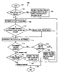
FIGS. l0A and lOB are flow diagrams 1000 and 1500, respectively, that
illustrate an approach for generating a routing stretch according to an
embodiment of
the invention. Referring first to FIG. 10A, after starting in step 1002, in
step 1004, a
determination is made whether the routing stretch is at the edge of the
routing region.
If so, then in step 1006, the routing stretch is redirected towards the end of
the
routing stretch along the edge of the routing region.
In step 1008, the distance to the next bend is determined. In step 1010, a
determination is made whether the determined distance is greater than the
distance to
the edge of the routing region. If so, then in step 1012, the determined
distance is
reduced to keep the routing stretch within the routing region.
In step 1014, the i-outing path is extended as far as possible, as described
in
more detail hereinafter with reference to FIG. 10B.
-28-
CA 02345443 2001-03-26
WO 00/23920 PCTIUS99/24454
In step 1016, a determination is made whether the determined distance was
achieved. If the determined distance was achieved, then in step 1018, a
determination is made whether the routing stretch has been completed. If the
routing
stretch was not completed, then in step 1020, the routing stretch is
redirected toward
the end of the routing stretch. Control then returns to step 1008 where the
distance to
the next bend is determined.
If in step 1016 the determined distance has not been achieved, then there is
an
obstacle in the way and iri step 1022, a determination is made whether all
feasible
redirects have been exhausted. If all feasible redirects have not been
exhausted, then
control proceeds to step 1026, where the routing stretch is redirected around
the
obstacle. Control then returns to step 1008 where the distance to the next
bend is
detennined.
A redirect is invalid if the redirect aims the routing path one hundred eighty
(180) degrees away from the end of the routing stretch, i.e., requires a U-
turn
afterward, or if the end of the routing path is outside the routing region
after making
the specified redirect.
If, in step 1022, all feasible redirects have been exhausted, then the
obstacle
conflict cannot be resolved and the process is complete in step 1024. In this
situation, obstacle resolution is performed in global routing to attempt to
resolve the
obstacle conflict.
If, in step 1018, the routing stretch is completed, then the process is
complete
in step 1024.
Referring to FIG. l OB, a flow diagram 1050 illustrates an approach for
extending a routing stretch according to an embodiment of the invention. After
starting in step 1052, in step 1054, an initial value of the current amount to
extend
the routing stretch is established. For example, the current amount may be set
to a
specified value. In step 1056, the routing stretch is extended by the current
amount.
In step 1058, a design rule check is performed on the extended routing stretch
to determine whether the applicable design rules are satisfied. In step 1060,
a
determination is made whether the design rule check was successful. If the
design
rule check was not successful, then in step 1062, a determination is made
whether the
simple routing indicator is asserted for the routing path. If the simple
routing
indicator is asserted, then no changes can be made to the surrounding layout
-29-
CA 02345443 2001-03-26
WO 00/23920 PCT/US99/24454
geometry and control proceeds to step 1064 where the current amount is reduced
by
a specified amount. Ther.t, in step 1066, a determination is made whether the
current
amount is zero. If the current amount is not zero, then control returns to
step 1056,
where the routing stretch is extended again, this time by the reduced current
amount
established in step 1064.
If in step 1062, the simple routing indicator is not asserted, then in step
1068,
changes are made to the surrounding layout geometry in an attempt to resolve
the
design rule check error. For example, as described herein, corner clipping may
be
employed or a source/drain contact moved to provide additional room for the
routing
stretch.
In step 1070, a detennination is made whether the changes were successful.
If the changes were not successful, then the current amount is reduced by the
specified amount in step 1064. Then, the determination is made in step 1066
whether the current amount is zero. If the current amount is not zero, then
control
returns to step 1056 where the routing stretch is extended by a lesser amount.
If in step 1060 the design rule check is successful, or in step 1070 the
changes
made to the surrounding geometry successfully resolved the design rule check
error,
or in step 1066 the current amount is zero, then the process is complete in
step 1072.
Note that in the situation where the process is completed because the current
amount
is zero, via step 1066, then the routing stretch could not be extended within
the
applicable design rules arid redirection or global routing is used to try to
resolve the
conflict. If the current amount returned is less than the initial value, step
1016 of
Figure 10A will note that the determined distance was not achieved, and step
1022
will be executed. If another feasible redirect is possible, the final design
rule check
error is used in step 1026 to determine the obstacle avoidance direction.
According to one embodiment of the invention, the routing of a new wire is
performed in the context of generating a "routing path." As defined herein, a
routing
path implements a connection between two join points as a wire on a single
layer
with no width changes. If a determination is made during global routing that
the
width of a wire is to be changed, then a branch join point is inserted with no
side
connections to allow the incoming wire to have a different width than the
outgoing
wire.
-30-
CA 02345443 2001-03-26
WO 00/23920 PCTIUS99/24454
Every edge in the node graph (i.e. the one created during global routing) has
a
routing path. Each routing path has a layer number, a wire width, a list of
strategies
used to guide detailed routing and one or two polygons that represent the
actual
routing for the wire. Detailed routing may proceed from either end of the
edge, or
even both ends if the atternpt from one end fails to reach the other (the
stretch in
between is referred to herein as an "unroute" and routing from both ends
reduces the
length of the unrouted section, sometimes allowing it to be completed), and
there is
one polygon per attempted end.
i. Moving Connection Points of Wires During Detailed Routing
As previously described herein, routing reference points are provided to guide
the routing of new wires to join points. Nevertheless, wires are not required
to be
connected only to the routing reference points, but can be connected to other
locations, as determined during detailed routing. FIG. 11 is a block diagram
that
illustrates changing connection points during detailed routing within the
constraints
of a set of applicable design rules according to an embodiment of the
invention.
An array of contacts join point 1100 includes four contacts, identified by
reference numerals 1102, 1104, 1106 and 1108. Theoretically, a wire may be
electrically connected to any location on array of contacts join point 1100.
However,
design rules limit the specific locations and/or angles or directions from
which a wire
may be connected to array of contacts join point 1100. For example, wires 1110
and
1112 can be connected to array of contacts join point 600 without violating
any
design rule spacing requirements. However, wire 1114 cannot be connected to
contact 1104 from the illustrated direction since this would result in an
acute angle
between wire 1114 and array of contact join point 1100 as indicated by arrow
1116,
which would violate desil,m rule spacing requirements. Similarly, wires 1118
and
1120 cannot be connected to array of contacts join point 1100 due to spacing
violations. That is, connecting wire 1118 or wire 1120 to array of contacts
join point
I 100 in the manner illusti=ated in FIG. 11 would cause a design rule spacing
requirement violation because of the acute angle between wire 1118 and 1120,
respectively, and array of contact join point 1100, as indicated by arrows
1122 and
1124, respectively.
-31-
CA 02345443 2001-03-26
WO 00/23920 PCT/US99/24454
As another example, suppose a wire (not illustrated) is to be connected to a
routing target 1126 on contact 1108. Given a wire width indicated by arrows
1128
and minimum spacing requirements indicated by arrows 1130, a test area 1132 is
defined for relocating the wire during detailed routing. If any geometry of
the join
point extends into the test area, the routing target site is illegal.
During detailed routing, the integrated circuit layout may be changed and join
points may be moved to allow a wire to be successfully routed from a starting
join
point to an ending join point, or otherwise as necessary to satisfy applicable
design
rules. According to one embodiment of the invention, three types of changes
are
allowed including clipping the corner of a contact enclosure, clipping the
corner of a
transistor island and moving a join point. Clipping the corner of a contact
enclosure
has been previously described herein. Generally, corner clipping is performed
whenever possible and the wire extended again. If no further progress is made,
then
the change is undone and the wire is bent as described in more detail
hereinafter.
FIG. 12 is a block diagram 1200 that illustrates an approach for clipping the
corner of a transistor island according to an embodiment of the invention. For
purposes of this example, a polysilicon wire 1202 is being extended along a
route
1203 between an obstacle on polysilicon 1204 and a transistor island comprised
of a
diffusion region 1206, a polysilicon gate 1208 and a source/drain contact
1209.
Since the minimum required spacing between diffusion and polysilicon would not
be
satisfied in the region indicated by reference numeral 1210, a portion 1212 of
diffusion region 1206 is removed, forming a new diffusion region boundary 1214
that satisfies the diffusion source/drain extension rule, as indicated by
reference
numeral 1216.
Clipping the corner of a contact enclosure or a transistor island can occur
only if permitted by the applicable design rules. Moving a join point, within
the
constraints specified by the applicable design rules, can be performed during
detailed
routing only if the join point is movable, i.e., is not a transistor gate or a
port, and has
no wires attached to it. Wires are not ripped up during detailed routing.
Rather, as
previously described, an attempt is made to generate a complete wire from the
starting join point to the ending join point and if the wire cannot be
completed, e.g.,
because of an obstacle that cannot be circumvented, then obstacle resolution
is
pursued during global routing. According to one embodiment of the invention,
when
-32-
CA 02345443 2001-03-26
WO 00/23920 PCT/US99/24454
a wire cannot be successfully routed from a starting join point to an ending
join point
during detailed routing, then an error code is provided to global routing that
indicates
the reason why the routing could not be successfully complete. For example,
the
error code might indicate a design rule check violation that would occur if
the wire
were extended any further.
A special type of join point move, one appropriate only to a layout synthesis
system, is to adjust a transistor source/drain contact placement within the
limits
calculated by the gate optimizer. FIGS. 13A and 13 B are block diagrams that
illustrate adjusting transistor source/drain contact placement to accommodate
the
routing of a new wire according to an embodiment of the invention. In FIG.
13A, a
transistor island 1300 includes a diffusion region 1302 and a polysilicon gate
1304
routed between source/drain contact join points 1306 and 1308 that each
include a
top metal layer. A metal wire 1310 is to be routed between source/drain
contact join
points 1306 and 1308 alor.kg a path 1311. However, this cannot be accomplished
without violating minimuin metal-to-metal spacing requirements. Specifically,
wire
1310 will violate the miniimum spacing requirement indicated by reference
numeral
1312 and will actually make contact with source/drain contact join point 1308
at
location 1314.
According to an embodiment of the invention, the routing of wire 1310
between source/drain cont.act join points 1306 and 1308 is achieved as
illustrated in
FIG. 13B by moving source/drain contact join points 1306 and 1308 apart, as
indicated by arrows 1316 and 1318, respectively, so that the metal-to-metal
minimum spacing requirements are satisfied, as indicated by arrows 1320 and
1322.
Note that the corners of source/drain contact join points 1306 and 1308
closest to
wire 1310 could also be clipped to provide additional space to route wire
1310.
Moving a contact join point in the manner just described can increase the
source/drain resistance of the transistor. Therefore, according to one
embodiment of
the invention, if further progress is not possible after moving a join point,
the join
point is moved back to its original location and the wire is bent instead. If
progress
is made, the change is stoi-ed in the change list for the wire being extended,
as
described in more detail. hereinafter.
As previously described, transistors can be spread apart within a single
transistor island or entire transistor islands spread apart during global
routing. These
-33-
CA 02345443 2001-03-26
WO 00/23920 PCT/US99/24454
are costly changes and are preferably performed during global routing because
they
require that existing wiririg be ripped up.
ii. Change Lists
Change lists are used to record changes made to integrated circuit geometry
while routing new wires during detailed routing. According to one embodiment
of
the invention, two change: lists are generated for each new wire. One of the
change
lists records changes made (in order) to the integrated circuit layout
geometry as a
new wire is extended frorn the starting join point to the ending join point.
The other
change list records changes made (in order) to the integrated circuit layout
geometry
as the new wire is extended from the ending join point to the starting join
point.
Recall that a wire may be routed from the starting join point towards the
ending join
point, from the ending join point towards the starting join point, or both. In
the event
that the two wires meet, successfully completing the routing, then the
polygons and
change lists are combined. According to one embodiment of the invention, one
of
the change lists is appended onto the other in reverse order so that all
changes are in
sequence when read from the specified end towards the other.
According to one embodiment of the invention, each change is characterized
by a change type, an object pointer, any parameters required for the change
operation
(such as a corner location), and the status of the object prior to the change
(e.g. the
previous amount of clipping, since enclosures can be clipped a bit at a time).
iii. Bending Wires
If a wire cannot be successfully routed even after clipping corners of a
transistor island or a join point or by moving a join point out of the way,
then the
new wire is bent. Because the wire is being extended at a known end, the
nature of
the design rule violation can be used to determine the preferred bend
directions for
obstacle avoidance. The canonical direction is determined by the design rule
check
performed in step 1060 of FIG. l OB. For example, according to one embodiment
of
the invention using a wire; comprising directed wire segments, the preferred
bend
direction is determined as described hereinafter with reference to FIGS. 14A-
14H.
Note that the bend directions here are determined for steps 1022 and 1026 of
FIG.
10A.
-34-
CA 02345443 2001-03-26
WO 00/23920 PCT/US99/24454
As illustrated in FIG. 14A, if the canonical direction from the end of a
routing
path 1400 to an obstacle 11402 is up and right, as indicated by arrow 1404,
then the
only allowable bend direction for routing path 1400 is up and to the left as
illustrated
in FIG. 14B, e.g., a forty-five degree bend. Any other direction would result
in a U-
turn which would require the routing path 1400 to be backed up and an earlier
bend
inserted.
As illustrated in FIG. 14C, if the canonical direction from the end of routing
path 1400 to obstacle 1402 is up and left, as indicated by arrow 1406, then
the only
allowable bend direction for routing path 1400 is up and to the right, as
illustrated in
FIG. 14D, e.g., a forty-five degree bend.
As illustrated in FIG. 14E, if the canonical direction from the end of routing
path 1400 to obstacle 1402 is up, then the bias direction is examined to
determine the
preferred bend direction. If the bias direction is towards the left, then, as
illustrated
in FIG. 14E, routing path 1400 is bent to the left, e.g., with a ninety degree
bend to
the left. If the bias directiion is towards the right, then, as illustrated in
FIG. 14F,
routing path 1400 is bent to the right, e.g., with a ninety degree bend to the
right.
If routing path 1400 cannot be extended in the preferred direction due to
further obstacles or becau.se routing path 1400 has reached the edge of a
valid region,
i.e., by exceeding the straying limit, then the reverse direction is attempted
before
failing. For example, a right ninety degree bend 1408 (FIG. 14E) if the bias
direction
is left and a left ninety degree bend 1410 (FIG. 14F) if the bias direction is
right.
As illustrated in FIG. 14G, if the canonical direction from the end of routing
path 1400 to an obstacle 1412 is left, then the detailed routing of routing
path 1400 is
backed up and a bend to the up and right is inserted, as illustrated by
reference
numeral 1414. If a bend to the up and right does not successfully circumvent
obstacle 1412, then a right bend is inserted in routing path 1400 as
illustrated by
reference numeral 1416.
As illustrated in FIG. 14H, if the canonical direction from the end of routing
path 1400 to obstacle 1412 is right, then the detailed routing of routing path
1400 is
backed up and a bend to the up and left is inserted, as illustrated by
reference
numeral 1418. If a bend to the up and left does not successfully circumvent
obstacle
1412, then a left bend is inserted in routing path 1400 as illustrated by
reference
numeral 1420.
-35-
CA 02345443 2001-03-26
WO 00/23920 PCT/US99/24454
d. Join Point Design Rule Checking
According to an embodiment of the invention, each layout polygon is tagged
with identifying information, such as a type code and object indices, so that
design
rules may be checked effectively during detailed routing. For example, a
transistor
gate polygon has a type transistor island geometry (that it is a transistor is
known
from the layer it is on) and indices denoting which island contains the
transistor gate
and the location of the transistor gate within the island. Transistor
source/drain
contacts, well ties and diffizsion polygons also have this type. Routing join
point
polygons have type join point and indices for the node number and point index
within the graph representing the node. Routing path polygons have type
routing
path, an index for the node number and an index for the edge number within the
graph. Other geometry, such as wells, implants, supply polygons, and perimeter
(bounding) polygons would also have identifying types and tags. Thus when a
design rule check is unsuccessful, the two affected polygons are used to
determine
the nature of the violatior.i as well as implement high-level avoidance
strategies. For
example, if a polysilicon ~wire approaches the diffusion polygon of a
transistor island,
detailed routing would stop and the violation would be returned to the global
router,
which then either increases the straying limit for the routing stretch,
generates hint
polygons to guide routing around the transistor island, changes the routing
layer to
one which may cross over a transistor island, or backs off and tries another
direction.
According to one embodiment of the invention, two types of design rule
checks are performed: a join point design rule check and a routing path design
rule
check. The join point design rule check evaluates the geometry of a join point
with
respect to the surrounding layout geometry. The routing path design rule check
evaluates the geometry of a routing path (or a section thereof) with respect
to the
surrounding layout geometry, as described in more detail hereinafter. Because
geometry is always added to a region that meets design rules, any identified
design
rule errors are a direct result of the new layout geometry, even if the design
rule
errors are between unrelated layout geometry elements. For example, this
occurs
when the addition of a join point or routing path causes a dogbone spacing
rule to be
violated. FIG. 15 is a block diagram 1500 illustrating the violation of a
dogbone
spacing rule attributable to an extension of a routing path. Diagram 1500
includes a
newly extended (metal) routing path 1502 adjacent to contact enclosures 1504
and
-36-
CA 02345443 2001-03-26
WO 00/23920 PCT/US99/24454
1506. For purposes of explanation, a typical spacing requirement may require a
minimum of four units of separation between contact enclosures 1504 and 1506,
as
indicated by arrow 1508. An exception to this requirement is the so called
"dogbone" rule which provides for an exception to the normal minimum spacing
requirement and allows contact enclosures 1504 and 1506 to be closer together,
so
long as either contact enclosure 1504 or 1506 does not have a specified amount
of
one of its edges adjacent to another layout element. Thus, in the present
example, if
routing path 1502 were not present and contact enclosures 1504 and 1506
evaluated
on their own, they would violate the standard spacing requirement, but would
satisfy
the dogbone exception. However, the amount of the lower edge of contact
enclosure
1504 that is adjacent to routing path 1502, represented by reference numeral
1510,
exceeds the specified amount. As a result, the presence of routing path 1502
causes a
spacing violation between enclosure contacts 1504 and 1506 that did not exist
prior
to the extension of routing path 1502 adjacent to contact enclosure 1504. It
should
be noted that a looser definition of edge length that considers only two
objects at a
time does not result in this type of spacing error. However, it is sometimes
preferable to perform a worst case evaluation.
An example of a join point design rule check implemented in pseudo code
according to an embodiment of the invention includes the following steps:
for each layer in the join point do
for each attached wire on the layer do
if the "approach" flag for the wire end is not set then
add the routing path polygon for the wiring end to an exclusion list
endif
if the "short path" flag for the graph edge of the wire is set then
add all polygons for the join point at the other end of the edge to an
exclusion list
endif
end # each attacheci wire
for each polygon near the join point polygon do # on all layers
compute the spacing between the two polygons according to the types of
polygon, the layer numbers, and the design rules
-37-
CA 02345443 2001-03-26
WO 00/23920 PCT/US99/24454
if a spacing does apply then
if the polygons are too close together then # including definite dogbone
error
return that error
endif # too close
if the nearby polygon is on this layer and
the nearby polygon is part of a join point and
the polygons might be too close together and # i.e. might violate
dogbone
errors are being accumulated then
remember the nearby join point
endif
endif # spacing applies
compute the enclosure between the two polygons according to the types of
polygon, the layer numbers, and the design rules
if an enclosure does apply and the polygons do not meet the rule then
return that error
endif
end # each polygon
end # each layer
if errors were accumulated and nearby join points may violate a dogbone rule
then
for each possibly violating nearby join point do
run a join point DRC around that join point without accumulating further
errors
if a violation was found then
return that violation # even though it may not refer to the new geometry
endif
end # each possibly violating join point
endif # may have violated
The computations required to check the correctness of spacing or enclosure,
performed by an object passed to a generic spacing or enclosure checking
routine,
depend upon the design rules, the layer numbers, the polygon types, the wire
width
-38-
CA 02345443 2001-03-26
WO 00/23920 PCT/US99/24454
of each polygon, the edge; length of each polygon, and whether the polygon
near the
join point is in any exclusion lists. For example, if the nearby polygon is a
wide
routing path, then the spacing requirement may be larger than normal unless
the edge
length of at least one of the two polygons is less than the dogbone edge
length in the
design rules. Other custom rule evaluations are possible as well, such as
dogbone
edge length requirements between wires of normal width or an extra spacing
between
polysilicon interconnect and transistor source/drain contacts.
According to one embodiment of the invention, the "worst" design rule
violation is identified, as determined by specified criteria such as the
distance the
new data must be moved in order to fix the violation. Thus each violation
found
would be compared with the current worst, and the worst violation would be
returned
at the end of the procedure.
The exclusion list applies to intralayer spacing checks for routing layers
within the join point and interlayer enclosure checks for contact layers
within the join
point. If the two polygor.Ls are on the same routing layer and the nearby
polygon is in
the exclusion list, no spacing applies. If the join point polygon is on a
contact layer
and the nearby polygon is in the exclusion list, e.g., part of the same join
point, then
no enclosure applies. This allows the join point to reduce temporarily the
enclosure
around the contact when defining a wire attachment, knowing that the enclosure
rule
requirements will be met as soon as the routing path is drawn. For example,
FIG. 16
is a block diagram 1600 that illustrates the approach of reducing temporarily
the
enclosure around the contact when defining a wire attachment. Diagram 1600
includes a contact enclosure join point 1602 with a reduced enclosure,
indicated by
reference numeral 1604, and a routing target 1606. The enclosure rule
requirements
are satisfied when a routing path 1608 is attached to contact enclosure join
point
1602.
According to one embodiment of the invention, after a design rule check is
performed, those join points that might possibly violate design rules are
identified
and remembered. For example, this occurs when a dogbone spacing violation
might
have occurred at a particular join point. If the nearby join point definitely
violates a
dogbone spacing rule to the join point being checked, that error is identified
immediately. Otherwiseõ a join point design rule check is performed later for
that
join point to see if the tot:al edge length in violation exceeds the design
rule limit. To
-39-
CA 02345443 2001-03-26
WO 00/23920 PCT/US99/24454
avoid infinite recursion, this join point design rule check does not identify
nearby
join points that might also violate the design rules. Rather, it is performed
only
because a single join poirit DRC does not consider all combinations of
spacings, but
only those that reference the join point under test.
e. Approaching Indicators for Design Rule Checking
It is necessary to ensure that routing paths do not come too close, i.e.,
violate
spacing rules, to portions of join points other than routing targets.
Therefore,
according to one embodiinent of the invention, each end of a routing path has
an
associated approaching iridicator (flag). When the approaching indicator is
asserted
(set) for a particular end, then the routing path has not yet reached the join
point and
spacings between the routing path and the join point may be checked,
especially
locations other than the routing target. This ensures that the routing path
does not
violate a spacing rule for a part of the join point other than the routing
target. Note
that the design rule checks associated with join points ensure that routing
targets for
attached wires do not create design rule violations, except when the routing
path is
long enough to bend.
Once it is known that a routing path will not cause any design rule violations
with the join point, the approaching indicator for the routing path is
deasserted. Then
the routing path is extended to abut the routing target on the join point, and
subsequent routing path DRCs exclude the join point routing polygons from
consideration.
FIGS. 17A and 17B illustrate the use of approaching indicators according to
an embodiment of the invention. In FIG. 17A, a routing path 1700 is being
extended
towards a contact enclosure join point 1702 and a routing target 1704. At this
point,
the approaching indicatoi- for routing path 1700 is asserted and the spacing
1706
between routing path 1700 and routing target 1704 checked against applicable
design
rules. In FIG. 1.7B, the approaching indicator for routing path 1700 is
deasserted
(cleared) and consequently, the spacing between routing path 1700 and contact
enclosure join point 1702 is not checked.
f. Short Path Indicators for Design Rule Checking
In some situations, a routing path connects two join points, in particular
contact enclosure join points, that are close enough to each other to prevent
a
-40-
CA 02345443 2001-03-26
WO 00/23920 PCT/US99/24454
meaningful design rule check of the routing path from being performed.
Similarly,
the close proximity of the join points causes a design rule check of either
join point
to exclude the routing polygons for the other join point. The wire between the
two
join points, if any (they may abut), may be drawn wider than normal to avoid
"notch"
violations as well.
For example, in FIG. 18, two contact enclosure join points 1800 and 1802 are
connected by a routing path 1804. Routing paths 1806 and 1808 are connected to
contact enclosure join points 1800 and 1802, respectively. In this example,
the close
proximity of contact enclosure join points 1800 and 1802 violates a minimum
spacing rule for contact enclosures, as indicated by reference numeral 1810,
making
a design rule check of contact enclosure join points 1800 and 1802 or routing
path
1804 impractical.
In other situations, a single join point integrates two contacts for
connecting
two non-adjacent routing layers, e.g., first metal and third metal, when the
contacts
cannot be placed directly on top of each other. In these situations, the close
proximity of the contacts prevents a meaningful design rule check from being
performed. Referring again to FIG. 18, in this situation for example, routing
path
1806 could be on a first metal layer, routing path 1804 on a second metal
layer and
routing path 1808 on a third metal layer. In this situation, contact enclosure
join
point 1800 would connect the first and second metal layers and contact
enclosure
join point 1802 would connect the second and third metal layers.
In view of the particular problems associated with very short routing paths
between join points, according to an embodiment of the invention, these types
of
short paths are identified by a short path indicator. When the short path
indicator for
a routing path is asserted, then the routing path is a short routing path and
the
conventional routing path and join point design rule checks are not performed.
Instead, the routing path and connected join points must be "correct by
construction."
g. Routing Path Design Rule Checking
An example of a routing path design rule check implemented in pseudo code
according to an embodiment of the invention is provided hereinafter. The
design
rule check of a routing path is similar to the design rule check of a join
point except
-41-
CA 02345443 2001-03-26
WO 00/23920 PCT/US99/24454
that the routing path has only a single layer and precisely two end join
points, as
opposed to an arbitrary nrunber of attached edges.
build a Test Polygon from the routing path polygon
if the "approach" flag for the first end is not set then
add all polygons in the join point at the first end to an exclusion list
for each other routing path attached to the first join point do
if the other routing path is on the same layer as the current routing path and
the "approach" flag for this end of the other routing path is not set then
add the near portion of the other routing path polygon to an exclusion list
if the other routirig path has the "short path" flag set then
add all polygor.ts in the join point at the other end of the other routing
path
to
an exclusion list
endif # short path
endif # on same layer
end # all other paths
endif
if the "approach" flag for the second end is not set then
add all polygons in the join point at the second end to an exclusion list
for each other routing path attached to the second join point do
if the other routing path is on the same layer as the current routing path and
the "approach" flag for this end of the other routing path is not set then
add the near portiion of the other routing path polygon to an exclusion list
if the other routir.ig path has the "short path" flag set then
add all polygons in the join point at the other end of the other routing path
to
an exclusion list
endif # short path
endif
end # all other paths
endif
for each polygon near the Tested Polygon do # on all layers
-42-
CA 02345443 2001-03-26
WO 00/23920 PCTIUS99/24454
compute the spacing between the two polygons according to the types of
polygon,
the layer numbers, and the design rules
if a spacing does apply then
if the polygons are too close together then # including definite dogbone
error
return that error
endif # too close
if the nearby polygon is on this layer and
the nearby polygon is part of a join point and
the polygons might be too close together and # i.e. might violate dogbone
errors are being accumulated then
remember the nearby join point
endif
endif # spacing does apply
compute the enclosure between the two polygons according to the types of
polygon,
the layer numbers, and the design rules
if an enclosure does apply and the polygons do not meet the rule then
return that error
endif
end # each polygon
if errors were accumulated and nearby join points may violate a dogbone rule
then
for each possibly vic-lating nearby join point do
run a join point DRC around that join point without accumulating further
errors
if a violation was found then
return that violation # even though it may not refer to the new geometry
endif
end # each possibly violating join point
endif # may have violated
-43-
CA 02345443 2001-03-26
WO 00/23920 PCT/US99/24454
The test polygon comprises enough of the routing path polygon to ensure that
any newly created dogbone violations are reported. Specifically, the test
polygon
includes all of the newly extended routing path geometry plus a length of the
existing
wire that is at least as long as the dogbone edge length limit. This value is
determined by the need to detect a dogbone spacing violation caused by the
first unit
of wire extension.
According to one embodiment of the invention, the entire routing path
polygon may be used for the routing path design rule check, although this may
be
computationally expensive if the routing path is very long, for example in a
in a chip-
level router. It is generally more efficient to test a (relatively) small
piece of the
routing path and "move" it along the routing path being constructed.
The required spacings and enclosures are computed in the same way as for
the join point design rule check. Again, the exclusion list is used for
intralayer
spacing checks to prevent the reporting of violations between the routing path
and
the join points at each end.
If the approaching indicator is not asserted for an end of a routing path, the
routing path may violate spacing rules with respect to other routing paths
that are
approaching the same join point on the same layer. As a result, a portion of
those
routing paths must be excluded from the design rule check.
FIG. 19 is a block diagram 1900 that illustrates this situation. Routing paths
1902 and 1904 connect to contact enclosure join point 1906. In this situation,
a
design rule minimum spacing requirement is violated by the proximity of
routing
paths 1902 and 1904, as indicated by arrow 1908. Similarly, routing paths
1910,
1912 and 1914 connect to a branch join point 1916. In this situation, a design
rule
minimum spacing requirement is violated by the proximity of routing paths 1910
and
1912, as indicated by arrow 1918. Furthermore, a design rule minimum spacing
requirement is violated by the proximity of routing paths 1912 and 1914, as
indicated
by arrow 1920.
Therefore, according to an embodiment of the invention, a final wire segment
of the routing path is not checked against the final wire segments of the
other routing
paths attached to the same join point. This excludes only false errors because
wire
segments are convex and the final wire segment must be at least as long as the
spacing rule. For example, in FIG. 20, a routing path 2000 comprising wire
-44-
CA 02345443 2001-03-26
WO 00/23920 PCT/US99/24454
segments 2002 and 2004 and a routing path 2006 comprising wire segments 2008,
2010 and 2012 are attached to a contact enclosure join point 2014. According
to an
embodiment of the invention, spacing checks are not performed between wire
segments 2002 and 2008. However, spacing checks are performed between wire
segment 2004 and wire segments 2008, 2010 and 2012. Similarly, spacing checks
are performed between wire segment 2010 and wire segments 2002 and 2004. Also,
spacing checks are performed between wire segment 2012 and wire segments 2002
and 2004.
If a routing path attached to a join point at an end of the first routing path
has
the short path indicator asserted, then there may be false spacing violations
between
the first routing path and the second join point. FIG. 21 illustrates two
contact
enclosure join points 2100 and 2102 connected by a routing path 2104. A
routing
path 2106 is connected to contact enclosure join point 2100. In this
situation, a
design rule check applied to routing path 2106 may falsely identify a spacing
error
2108 between routing paths 2106 and 2104 and a spacing error 2110 between
routing
path 2106 and join point 2102. According to one embodiment of the invention,
detailed routing ensures no true violations occur between routing path 2106
and
contact enclosure join point 2102, for example, by allowing only certain types
of
adjacency between join points. For example, a transistor gate join point may
have a
straight branch join point attached to it when the gate join point is known
not to
curve back around such that it would interfere with the branch join point. Two
single-contact join points may be placed adjacent to each other if for example
a
connection is to be made from polysilicon to the first metal layer in the
first join
point and from the first metal layer to the second metal layer in the second
join point.
Wires attached to the firsl: join point on the first metal layer would
otherwise have
false violations reported to the second join point.
Once again, the addition of new geometry to the routing path may cause
violations to appear on nearby join points, so it is necessary to run join
point design
rule checks centered around these join points in order to determine whether
any
dogbone violations are now present.
-45-
CA 02345443 2001-03-26
WO 00/23920 PCT/US99/24454
h. Tight Routing Situations
There are situations where two join points are so close together that there is
insufficient room to site a routing path for an approach design rule check.
For
example, this occurs wheri two join points are just a bit further apart than
the spacing
rule, or the attachment directions are so constrained that the ends of the
routing path
to be completed cannot be aligned, or a hint polygon is placed very close to a
join
point or another hint polygon because of a restricted routing environment. In
these
situations, detailed routing might not be able to complete the routing path or
routing
stretch.
Therefore, according to one embodiment of the invention, if the distance to
be routed is less than a specified multiple of the wire width, e.g., four
times, a
special-purpose tight routing approach is used to construct the routing
stretch (or
routing path) in one step, with no gaps between the routing path and the join
points
or hint polygons at its ends. Then a routing path design rule check is
performed on
the routing path with the approaching indicators deasserted to identify any
design
rule violations. If a design rule violation is detected somewhere along the
constructed routing path, then an attached wire or hint polygon may be moved
to
cure the design rule violation. In certain situations, e.g., a one hundred
thirty-five
degree bend, the shape of the routing path can be changed to remedy the design
rule
error, either by selecting locations for the bends or by converting ninety
degree
(orthogonal) bends into separate forty-five degree (non-orthogonal) bends.
FIGS. 22A and 22B illustrate the use of the tight routing approach according
to one embodiment of the invention. Specifically, in FIGS. 22A and 22B, a
routing
path is required between contact enclosure join points 2200 and 2202. In FIG.
22A,
contact enclosure join points 2200 and 2202 are connected by a jogged (non-
orthogonal) routing path 2204. In FIG. 22B, contact enclosure join points 2200
and
2202 are connected by a bent (non-orthogonal) routing path 2206.
The tight routing approach is particularly useful when an attachment direction
is constrained, e.g., at a transistor gate end, and the join point or hint
polygon is
offset to the side. For example, in FIG. 22C, a bent routing path 2208,
generated in
accordance with an emboc[iment of the invention, connects a transistor gate
join point
2210 and a hint polygon (with routing direction) 2212.
-46-
CA 02345443 2001-03-26
WO 00/23920 PCT/US99/24454
The tight routing approach is also useful when a wire attached to a join point
is offset all the way to a corner. In this situation, the routing path may be
bent before
the spacing rule is met because no notch would be formed between it and the
join
point. Normally the routing path must travel far enough from the join point to
meet
the spacing rule before bending. However, if another routing path is attached
near
the location of the bend a violation will be created. For example, in FIG.
22D, a
routing path 2214 connects a contact enclosure join point 2216 to a hint
polygon that
is offset from contact enclosure join point 2216 in a corner. In FIG. 22E, a
routing
path 2220, generated in accordance with the tight routing approach, connects
hint
polygons 2222 and 2224.
The tight routing approach is also useful when a U-turn must be made, for
example, to connect two adjacent gate ends. This may be used even though
detailed
routing stops when a U-turn is required to prevent excessive searches. FIG.
22F
illustrates the use of the tight routing approach to generate a routing path
2226 that
connects transistor gate join points 2228 and 2230. Note that since other
routing
paths attached to the join point on the same layer are excluded from
consideration in
the routing path design rule check, the tight routing approach must not
request that a
wire be attached to a join. point unless there are no nearby attached wires on
that
layer.
6. OBSTACLE AND INSUFFICIENT SPACE RESOLUTION
In the event that a wire cannot be routed because of an obstacle or
insufficient
space, then steps are taken to resolve the obstacle conflict and/or provide
additional
space in the integrated ciircuit layout to route the wire. According to one
embodiment, any numbeir of several approaches are employed to resolve obstacle
conflicts and/or provide additional space. These include changing or adding
hint
polygons, changing the routing strategy, inserting one or more layer changes,
instructing the detailed router to backup and insert a bend, ripping-up and
rerouting
one or more wires, or routing the wire from the destination connection point.
Each
of these steps is described in more detail hereinafter.
a. Change or Add Hint Polygons
Global routing may change or add hint polygons to direct a routing path
around an obstacle during detailed routing. FIG. 23 is a block diagram 2300
that
-47-
CA 02345443 2001-03-26
WO 00/23920 PCT/US99/24454
illustrates adding a hint polygon to resolve an obstacle conflict according to
an
embodiment of the invention. Suppose a routing path needs to be routed between
contact enclosure join points 2302 and 2304. An obstacle 2306 prevents the
routing
of a straight path between. enclosure join points 2302 and 2304. In this
example,
detailed routing may not have been able to determine a design rule correct
route
between enclosure join points 2302 and 2304. In accordance with an embodiment
of
the invention, a hint polygon 2308 is added to guide the detailed routing of a
routing
path between enclosure join points 2302 and 2304.
b. Change Routing Strategy
Global routing may change the routing strategy for a particular routing path
by changing the simple routing indicator, by adjusting the straying limits, or
by
changing the bias direction. Disabling the simple routing flag can provide
additional
space by allowing surrouriding layout geometry to be moved or changed, e.g.,
by
clipping corners.
Adjusting, e.g., increasing, the straying limit for a routing path can allow a
routing path to be routed around an obstacle. Adjusting straying limits may be
required in conjunction with adding one or more hint polygons, depending upon
the
location of the new hint polygons. As illustrated in FIG. 23, the original
routing
region is indicated by reference numeral 2310. Thus, even though new hint
polygon
2308 has been added to guide the detailed routing of a routing path between
enclosure join points 2302 and 2304, the routing cannot be accomplished
without
increasing the straying liniits. Specifically, for the first stretch of the
new routing
path between enclosure join point 2302 and hint polygon 2308, the straying
limits are
increased as indicated by reference numeral 2312. For the second stretch of
the new
routing path between hint polygon 2308 and enclosure join point 2304, the
straying
limits are increased as indicated by reference numeral 2314.
FIG. 24 is a block diagram 2400 that illustrates another example of increasing
straying limits to avoid an obstacle according to an embodiment of the
invention.
Suppose a routing path is to be generated between enclosure join points 2402
and
2404. An obstacle 2406 prevents the routing of a straight path between
enclosure join
points 2402 and 2404. A routing path 2408 is started from enclosure join point
2402
but is stopped at boundary 2410 defined by the current straying limit, which
may be
-48-
CA 02345443 2001-03-26
WO 00/23920 PCT/US99/24454
zero. The intended routing path is represented by line 2412. According to an
embodiment of the invention, the straying limit is increased to provided a
larger
routing region 2414 which allows routing path 2408 to be extended around
obstacle
2406 and connect to contact enclosure join point 2404.
Global routing may also change the bias direction for a routing path so that
when it is routed, or ripped up and rerouted, it avoids as much as possible an
area
desired for use by another routing path. This is simpler than inserting hint
polygons.
For example, it may be desirable to route a path towards the left side of an
open
region, rather than the middle, to provide space for a contact join point to
be inserted
later.
c. Insert One or More Layer Changes
Global routing may insert one or more layer changes to route a routing path
over or under an obstacle. FIGS. 25A and 25B illustrate an approach for
avoiding an
obstacle by inserting one o:r more layer changes to route a routing path over
or under
an obstacle according to an embodiment of the invention. In FIG. 25A, a
routing
path is to be routed between contact enclosure join points 2500 and 2502.
Although
routing paths 2504 and 2506 can be extended from contact enclosure join points
2500 and 2502, an obstacle: 2508 prevents the routing from being completed.
In FIG. 25B, contact enclosure join points 2510 and 2512 are added and
connected to routing paths 2504 and 2506, respectively, to provide a layer
change to
a different layer than the layer on which obstacle 2508 resides. Then a
routing
stretch 2514 is added to connect contact enclosure join points 2510 and 2512.
For
example, if contact enclosure join points 2500 and 2502 and obstacle 2508 are
located on a first metal layer, then contact enclosure join points 2510 and
2512 can
provide a connection to a second metal layer, which can include routing
stretch 2514
to pass over obstacle 2508. The approach is also applicable to changing layers
to
route a routing stretch under and obstacle.
d. Instruct the Detailed Route to Backup and Insert a Bend
Global routing can also resolve an obstacle conflict by instructing the
detailed
routing to backup and insei-t a bend to route around an obstacle. FIG. 26 is a
block
diagram 2600 that illustrates the use of this approach to avoid an obstacle. A
routing
path 2602 is being extended towards an ending join point 2604, which in this
-49-
CA 02345443 2001-03-26
WO 00/23920 PCT/US99/24454
example is a contact enclosure join point. An obstacle 2606 prevents routing
path
2602 from reaching ending join point 2604. According to an embodiment of the
invention, global routing instructs detailed routing to backup to a specified
location
and reroute routing path along a different path, indicated by reference
numeral 2608.
e. Rip-Up and Reroute One or More Wires
Global routing may also rip up and reroute one or more routing paths to
resolve an obstacle conflict. Should global routing rip up a routing path for
strategic
reasons, the changes are removed from the change lists one by one and the
effects of
each change are undone if possible. For example, if a contact enclosure corner
was
clipped, the corner is restored if it would not cause new design rule check
violations
(later routing might have taken advantage of the clipped corner as well). If a
wire is
only partially ripped up, only those changes required for the wire section
removed
are undone.
As previously described herein, clipping the corner of a contact enclosure
may slightly reduce circuit production yield (a partially uncovered contact
may not
function properly, and clipping corners increases the odds that this may
occur), so it
is performed only when necessary to increase routing density and only in
crowded
areas. Similar logic applies to clipping transistor island corners or
adjusting
source/drain contacts; the transistor source/drain resistance may increase,
slowing
down the circuit slightly. Thus if a routing path is ripped up to make room
for
another wire, all of the join point and transistor island changes for that
routing path
are undone if possible. Routing added later may have taken advantage of the
changes, so a design rule check must be run when restoring geometry. If an
error is
found, the change is left behind. Later rip-up may in turn remove the newer
routing,
so when all routing is complete the transistor island and join point corners
are
examined again to see if any corner clips can be restored.
f. Route Wire From Destination Connection Point
The global router may also attempt to draw the routing path from the other
end; the
length of the unroutable section can then be used to help determine the
strategy to
apply. For example, if the length is very short, e.g., not much more than the
width of
a single wire, then it may be advantageous to rip up the one or two wires
intervening,
then force those wires to go over the new one. If the wire length is long,
e.g., a
-50-
CA 02345443 2001-03-26
WO 00/23920 PCT/US99/24454
substantial fraction of the minimum possible routing path length, then the
routing
path will probably need to use a different layer. This is because the cost of
removing
all of the intervening geoinetry on the current layer is likely to be high.
7. IMPLEMENTATION MECHANISMS
The approach for routing integrated circuits described herein is applicable to
any type of integrated circuit design system and is independent of the
particular
design rules employed by a particular system. Furthermore, the approach may be
implemented as part of an integrated circuit design system or as a stand-alone
routing
mechanism that interacts with a integrated circuit design system. The routing
approach described herein may be implemented in hardware circuitry, in
computer
software, or a combination of hardware circuitry and computer software.
Figure 27 is a block diagram that illustrates a computer system 2700 upon
which an embodiment of the invention may be implemented. Computer system 2700
includes a bus 2702 or other communication mechanism for communicating
information, and a processor 2704 coupled with bus 2702 for processing
information.
Computer system 2700 also includes a main memory 2706, such as a random access
memory (RAM) or other clynamic storage device, coupled to bus 2702 for storing
information and instructions to be executed by processor 2704. Main memory
2706
also may be used for stori:ng temporary variables or other intermediate
information
during execution of instructions to be executed by processor 2704. Computer
system
2700 further includes a read only memory (ROM) 2708 or other static storage
device
coupled to bus 2702 for storing static information and instructions for
processor 2704.
A storage device 2710, such as a magnetic disk or optical disk, is provided
and coupled
to bus 2702 for storing ini'orrnation and instructions.
Computer system 2700 may be coupled via bus 2702 to a display 2712, such as
a cathode ray tube (CRT), for displaying information to a computer user. An
input
device 2714, including alphanumeric and other keys, is coupled to bus 2702 for
communicating information and command selections to processor 2704. Another
type
of user input device is cursor control 2716, such as a mouse, a trackball, or
cursor
direction keys for communicating direction infornlation and command selections
to
processor 2704 and for controlling cursor movement on display 2712. This input
-51-
CA 02345443 2001-03-26
WO 00/23920 PCTIUS99/24454
device typically has two degrees of freedom in two axes, a first axis (e.g.,
x) and a
second axis (e.g., y), that allows the device to specify positions in a plane.
The invention is related to the use of computer system 2700 for routing
integrated circuits. According to one embodiment of the invention, the routing
of
integrated circuits is provided by computer system 2700 in response to
processor
2704 executing one or more sequences of one or more instructions contained in
main
memory 2706. Such instructions may be read into main memory 2706 from another
computer-readable mediLUn, such as storage device 2710. Execution of the
sequences of instructions contained in main memory 2706 causes processor 2704
to
perform the process steps described herein. One or more processors in a multi-
processing arrangement r.nay also be employed to execute the sequences of
instructions contained in main memory 2706. In alternative embodiments, hard-
wired circuitry may be used in place of or in combination with software
instructions
to implement the invention. Thus, embodiments of the invention are not limited
to
any specific combination of hardware circuitry and software.
The term "computer-readable medium" as used herein refers to any medium
that participates in providing instructions to processor 2704 for execution.
Such a
medium may take many forms, including but not limited to, non-volatile media,
volatile media, and transrnission media. Non-volatile media includes, for
example,
optical or magnetic disks, such as storage device 2710. Volatile media
includes
dynamic memory, such as main memory 2706. Transmission media includes coaxial
cables, copper wire and fiber optics, including the wires that comprise bus
2702.
Transmission media can also take the form of acoustic or light waves, such as
those
generated during radio wave and infrared data communications.
Common forms of computer-readable media include, for example, a floppy
disk, a flexible disk, hard disk, magnetic tape, or any other magnetic medium,
a CD-
ROM, any other optical medium, punch cards, paper tape, any other physical
medium with patterns of holes, a RAM, a PROM, and EPROM, a FLASH-EPROM,
any other memory chip or cartridge, a carrier wave as described hereinafter,
or any
other medium from which a computer can read.
Various forms of computer readable media may be involved in carrying one or
more sequences of one or more instructions to processor 2704 for execution.
For
example, the instructions may initially be carried on a magnetic disk of a
remote
-52-
CA 02345443 2001-03-26
WO 00/23920 PCT/US99/24454
computer. The remote computer can load the instructions into its dynamic
memory
and send the instructions over a telephone line using a modem. A modem local
to
computer system 2700 can receive the data on the telephone line and use an
infrared
transmitter to convert the data to an infrared signal. An infrared detector
coupled to
bus 2702 can receive the data carried in the infrared signal and place the
data on bus
2702. Bus 2702 carries the data to main memory 2706, from which processor 2704
retrieves and executes the instructions. The instructions received by main
memory
2706 may optionally be stored on storage device 2710 either before or after
execution
by processor 2704.
Computer system 2700 also includes a communication interface 2718
coupled to bus 2702. Communication interface 2718 provides a two-way data
communication coupling to a network link 2720 that is connected to a local
network
2722. For example, communication interface 2718 may be an integrated services
digital network (ISDN) card or a modem to provide a data communication
connection to a correspoariding type of telephone line. As another example,
communication interface 2718 may be a local area network (LAN) card to provide
a
data communication connection to a compatible LAN. Wireless links may also be
implemented. In any such implementation, communication interface 2718 sends
and
receives electrical, electromagnetic or optical signals that carry digital
data streams
representing various types of information.
Network link 2720 typically provides data communication through one or
more networks to other data devices. For example, network link 2720 may
provide a
connection through local network 2722 to a host computer 2724 or to data
equipment
operated by an Internet Service Provider (ISP) 2726. ISP 2726 in turn provides
data
communication services through the world wide packet data communication
network
now commonly referred to as the "Internet" 2728. Local network 2722 and
Internet
2728 both use electrical, electromagnetic or optical signals that carry
digital data
strearns. The signals through the various networks and the signals on network
link
2720 and through commtinication interface 2718, which carry the digital data
to and
from computer system 2700, are exemplary forms of carrier waves transporting
the
information.
Computer system 2700 can send messages and receive data, including
program code, through the network(s), network link 2720 and communication
-53-
CA 02345443 2001-03-26
WO 00/23920 PCT/US99/24454
interface 2718. In the Internet example, a server 2730 might transmit a
requested
code for an application program through Internet 2728, ISP 2726, local network
2722
and communication interface 2718. In accordance with the invention, one such
downloaded application provides for the routing of integrated circuits as
described
herein.
The received code: may be executed by processor 2704 as it is received,
and/or stored in storage device 2710, or other non-volatile storage for later
execution.
In this manner, computer system 2700 may obtain application code in the form
of a
carrier wave.
The novel approach described herein for routing an integrated circuit
provides several advantages over prior routing approaches. One advantage is
that
design rule checks may be performed on an object-specific basis. This provides
increased flexibility during verification of an integrated circuit design. One
benefit
of this increased flexibility is that it allows object-specific design rules
to be
employed, for example, in phase-shift masking applications to reduce line
width.
Another benefit of the increased flexibility is that the design rules for any
particular
object may change over time, independent of the design rules applied to other
objects
in a layout. This is particularly important for supporting "landing zone"
rules.
Prior art routers are incapable of making room for new wires except by
separating cells, i.e., by adding feedthroughs in a row of cells, or
transistor islands (in
an intracell router). By moving or modifying obstacles only enough to allow a
wire
to approach, more room is left to add wires on the other side. Thus the
routing for
the integrated circuit gene;rated in accordance with the present invention can
be made
more dense than is possible with a coarse-grid or orthogonal router.
The combination of an obstacle-moving detailed router and an obstacle-
avoiding global router promotes algorithmic simplicity, execution speed, and
router
capability. The global router need not set up strategies for individual
routing paths
until an obstacle is found, meaning that a large fraction of wires may be
routed
without intervention. Once an obstacle is found, the global router can use its
high-
level knowledge of major obstacles, e.g., transistor islands, to define an
evasion
strategy. The use of hint polygons and straying limits allows an efficient,
goal-
directed ("depth first") search mechanism without concern for the suboptimal
routing
common to this type of approach as used in conventional routing approaches.
The
-54-
CA 02345443 2001-03-26
WO 00/23920 PCT/US99/24454
algorithms of the detailed router are also simpler because they do not need to
consider layer changes or expend significant effort traveling around
obstacles. Major
changes are made by the global router; minor changes are made by the detailed
router. Furthermore, significant performance advantages are achieved by
partitioning tasks, e.g., design rule checks, between join points and routing
tasks.
Another advantage is provided by the tight routing mechanism described herein
to
handle tight routing situations.
In the foregoing specification, the invention has been described with
reference to specific embodiments thereof. However, various modifications and
changes may be made thereto without departing from the broader spirit and
scope of
the invention. The specification and drawings are, accordingly, to be regarded
in an
illustrative sense rather than a restrictive sense.
-55-