Note: Descriptions are shown in the official language in which they were submitted.
CA 02345591 2001-05-03
Igarashi 1-1-4-1-I-1 I
RF CONNECTOR WITH IMPEDANCE MATCHING TAB
BACKGROUND OF THE INVENTION
Field of the Invention
The present invention relates to adaptors, interfaces, and connectors used to
couple an electrical signal to an electrical component receiving the signal.
Description of the Related Art
There is a need to provide connection between signal sources and signal sinks,
i. e.
components receiving the electrical signal from the source. For example, a
signal
generator may generate a 10 Gb/S RF modulation signal, which is carried via
coax cable
i o to a modulator driver of a high speed laser module used for telecom
applications. The
driver helps to generate a modulated output laser beam which has a modulation
obtained
from the modulation signal.
At such high frequencies, it is important to provide for impedance matching
for
optimal electrical return loss, to minimize signal reflections and to optimize
system
is performance. In general, impedance matching means that the impedance of the
external
device (sink), as well as the transmission line, matches that of the source.
Improper
impedance matching can lead to excessive distortion and noise problems such as
signal
reflection. Thus, transmission lines such as coaxial cables are often used for
high-
frequency RF signals, to provide uniform and matched impedance between the
signal
a o source and sink.
However, the connections between the end of the transmission line and the end
component receiving the signal often introduce unwanted impedance into the
signal path,
thus causing signal reflection and adversely ai~ecting system performance. For
example,
in a high speed laser module telecom application, the coax cable from the
output of the
a s signal generator is plugged into the receiving (input) end of an adaptor
or connector such
as an RF connector, by a standard coax type interface. The output side of the
RF
connector has an unshielded center pin. When the connector is inserted into
the
CA 02345591 2001-05-03
Igarashi 1-1-4-1-1-1 2
appropriate receptacle of the laser module housing, the center pin (typically
about 0.7 mm
in length) is wire bonded to the modulator driver (signal sink). The driver
uses the RF
modulation signal carried by the coax cable to modulate a laser beam.
The coax cable can be designed to have a uniform impedance such as SOS2,,
s which matches an input impedance of SOS2 of the modulator driver. However,
there will
be an air gap between the face of the RF connector, along the exposed,
unshielded length
of the center pin, to the modulator driver. This mismatching will introduce
unwanted
signal reflections and other undesirable effects, thus degrading system
performance.
Previous attempts to address this problem involve use of discrete adaptors and
1 o interfaces from the end user's RF signal to the end component receiving
the signal.
However, using an increased number of pieces reduces overall performance, and
results
in higher cost and more complex end product manufacturing. Further, when
discrete
components are used, there is always an interface issue with associated
performance
degradation. Discrete components also increase performance variation.
i s SUMMARY
According to the present invention, a sub-miniature push-on RF connector is
provided for connecting a transmission line to a signal sink. The connector
has a
shielded transmission line section having a signal line and a ground line
extending axially
through the connector. A center pin is coupled to the signal line and extends
from the
a o center of a front face of the connector in an axial direction. A
semicircular tab coupled
to the ground line extends from the front face of the connector substantially
along the
length of the center pin and partially surrounding the center pin to reduce an
air gap
impedance, the tab having first and second wire bonding surfaces at the ends
of the
semicircular shape thereof and disposed adjacent to said center pin.
25 BRIEF DESCRIPTION OF THE DRAWINGS
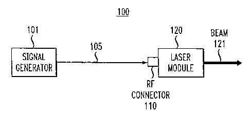
Fig. 1 is a block diagram of a system employing the improved RF connector of
the present invention;
CA 02345591 2001-05-03
Igarashil-1-4-1-1-1 3
Fig. 2 is a perspective view of the improved sub-miniature push-on (SMP), RF
connector with impedance matching tab of the system of Fig. 1, in accordance
with an
embodiment of the present invention;
Fig. 3 illustrates the SMP RF connector of Fig. 2 inserted into a receptacle
of a
s laser module of the system of Fig. 1; and
Fig. 4 is a top view illustration of the SMP RF connector of Fig. 2 wire
bonded
at its center pin and impedance matching tab to a modulator driver.
DESCRIPTION OF THE PREFERRED EMBODIMENT
Referring now to Fig. l, there is shown a block diagram of a system 100
i o employing an improved RF connector 110, having an impedance matching tab
for
improved impedance matching, connection, and signal transmission. As
illustrated, a
signal generator 101 produces a high frequency (e.g., 10 Gb/s) RF signal,
which is
carried by coax cable 105. Coax cable is attached to the input of RF connector
110, e.g.
by a bullet plug or standard coax interface. RF connector 110 of the present
invention
1 s is inserted into the appropriate receptacle of high-speed laser module
120, which
produces modulated output laser beam 121.
Referring now to Fig. 2, there is shown a perspective view of improved RF
connector 110 of Fig. 1, in accordance with an embodiment of the present
invention.
RF connector 110 is preferably a sub-miniature push-on (SMP) type RF
connector, also
a o comprising impedance matching tab 210. As illustrated, coax cable 105
attaches to the
back (input) end of SMP RF connector 110. At the front (output) end of RF
connector
110, center pin 201 extends for about 0.7 mm from front face 202.
Center pin 201 is electrically coupled at its base (at surface 202) to the
signal line
223 of a shielded transmission line section of connector 110, which extends
axially
25 through the connector housing. Shielded transmission line section also
comprises
shielding or ground line 222. Center pin 201 extends from the center of front
face 202
of the connector in an axial direction. In an embodiment, it is an extension
of signal line
223. At the other (back) end of connector 110, the shielded transmission line
section
CA 02345591 2001-05-03
Igarashi 1-1-4-1-1-1 4
terminates in a receptacle or input terminal 221 for mating to a shielded
transmission line
(coax line 105) having a signal line and a ground line. Thus, when coax line
105 is
plugged into the input terminal of connector 110, its signal line is
electrically coupled
with the signal line 223 of connector 110, and thus to the center pin 210, and
its ground
s line (i.e. shielding) is electrically connected to the ground line portion
222 of RF
connector's shielded transmission line section.
A semicircular, "U-shaped" impedance matching tab 210 extends from front face
202 of connector 210 substantially along the length of the center pin, and
partially
surrounding center pin 201 along the extent of the thickness of matching tab
210. Tab
i o 210 is electrically coupled to the ground line of the shielded
transmission line section of
connector 110, and thus to the RF ground of coax cable 105.
Tab 210 has two substantially flat and parallel end surfaces 21 l, 212, which
are
next and close to center pin 201. Surfaces 211, 212 may be referred to as
first and
second wire bonding surfaces, which are at the ends of the semicircular shape
of tab 210,
is and which are disposed adjacent to the center pin 201. End surfaces 211,
212 are
substantially aligned along lines radiating from center pin 201, so that wire
bonding may
be done on the top of center pin 201 and on top of nearby surfaces 211, 212.
In an
embodiment, surfaces 21 l, 212 are in a plane slightly higher than the exact
axial center
of pin 201, so that wire bonded onto the top of center pin 201 would be
substantially on
zo the same level as wire bonded on surfaces 211, 212. If surfaces 211, 212
are much
higher than the top of pin 201, it would be more difficult to wire bond pin
201 to an
input terminal of a signal. If surfaces 211, 212 are much lower than the top
of pin 201,
then it may be difficult to wire bond the surfaces 211, 212 to ground
terminals in the
same process as the wire bonding of center pin 201, and the level of shielding
and thus
25 protection from air gap impedance is reduced. Thus, connector 110 is an SMP
RF
connector for connecting a transmission line (105) to a signal sink (420 in
Fig. 4).
Referring now to Fig. 3, there is shown the SMP RF connector 110 assembled
in high speed laser module 120 of system 100. RF connector 110 is inserted
into a
CA 02345591 2001-05-03
Igarashi I-1-4-1-1-1 5
receptacle 307 of module 120. Other components of laser module 120 (such as
the
modulator driver and laser device) are not shown, for simplicity of
illustration. An
output laser beam is emitted via opening 305. Electrical contacts 303 provide
for
connection between other components and sources outside module 120 and the
s components contained therein, e.g. to the modulator driver.
Tab 210 partially surrounds the center pin 201 along center pin 201's length,
thereby reducing the air gap impedance that would otherwise be introduced by
the air
gap around center pin 201. As will be appreciated, tab 210 provides a good
deal of
shielding for center pin 201, because it partially surrounds and is so close
to center pin
i o 201. This significantly reduces the impedance that would otherwise be
introduced along
the air gap length of center pin 201, if it were completely unshielded, as in
prior art
connectors. Thus, the center pin and the air gap between the face 202 of the
connector
and the bonding to wires connected to the sink device, do not degrade
impedance
matching (introduce impedance, or impedance mismatch) to the extent that would
be the
1 s case in the absence of impedance matching tab 210. Thus, tab 210 helps to
ensure
impedance matching between source and sink, and along the transmission line.
Further,
tab 210 provides easy wire bonding access from the end component to the RF
ground,
due to the placement of surfaces 21 l, 212.
The housing of RF connector 110 has an outer portion 232 and inner portion
a o 23 l, in an embodiment. The inner portion 231, in an embodiment, has a
shoulder or
ledge which serves as a stop when RF connector 110 is inserted into receptacle
307 of
module 120. Outer portion 232 may have "timing flats" (not shown) manufactured
into
the sides thereof. As will be appreciated, these timing flats are opposing
flat surfaces in
the otherwise circular cross-section of outer portion 232, which may be used
for precise
a s alignment of RF connector 110, e.g. to align the RF connector parallel to
the package
base, as often required in telecom applications.
Referring now to Fig. 4, there is shown a top view illustration of the SMP RF
connector 110 wire bonded at its center pin 201 and impedance matching tab 210
to a
CA 02345591 2001-05-03
Igarashi 1-1-4-1-1-1 G
modulator driver 420. As shown, the signal input pin of driver 420 is bonded
by bonding
wire 401 to the top surface of center pin 201, near its tip (far end). The
ground
terminals of driver 420 are wire bonded to each of surfaces 211, 212, by
bonding wires
411, 412, respectively. In the implementation illustrated in Fig. 4, two
closely-spaced
s bonding wires 412 are used to connect to face 212 of impedance matching tab
210, and
two closely-spaced bonding wires 411 connect the ground of driver 420 to
surface 211
of impedance matching tab 210. In an alternative embodiment, different number
of
bonding wires may be employed to connect each of faces 211, 212 to the
corresponding
ground terminal of driver 420. For example, a single bonding wire may be
employed,
i o or three, or two pairs of two.
In Fig. 4, the length d2 represents approximately the distance from the face
202
of connector 110, in an axial direction, to approximately the end of center
pin 201,
approximately 0.7 mm. Length d3 represents the length from the end of pin 201
and the
outer face of tab 210 (roughly where the wires are bonded to these elements),
to the
i5 terminals of the sink device (driver 420). The length dl is the sum of d2
and d3, and
represents the distance from the face 202 of connector 110, in an axial
direction, to the
terminals of driver 420.
As shown, the use of impedance matching tab 210 reduces the air gap from
distance dl to the shorter distance d3. Further, the presence of impedance
matching tab
2 0 210 makes it possible to easily wire bond ground terminals of driver 420
to surfaces 21 l,
212, by bond wires 411, 412, respectively. Without impedance matching tab 210,
the
air gap over distance d2 would still be present, and it would be more
difficult to connect
the ground terminals of driver 420 to the RF ground. By eliminating the air
gap over
distance d2, and by providing precise and similar wire bond lengths for bond
wires 41 l,
2 5 412, 401, electrical return loss is optimized and the impedance of the
signal path remains
matched. Empirical results indicate that the use of impedance matching tab 210
significantly improves the performance in a high-speed telecom application,
over that
achieved when using a connector without an impedance matching tab.
CA 02345591 2001-05-03
Igarashi I-1-4-1-1-1 7
The SMP RF connector of the present invention thus provides for improved
impedance matching and performance, in a single package, without having to
employ a
discrete connector and matching element components. The present invention also
eliminates RF performance dependence on laser package vendors because the key
RF
s performance elements are embodied in a portable connector that requires only
a simple
hole in the package shell for installation. In addition, the SMP RF connector
has simple,
cost-effective timing flats to install the part in a package with the required
parallelism to
the package base. The physical requirements and tolerances on the package are
therefore minimized, allowing for substantial cost reduction of the package
body.
1 o In an alternative embodiment, pin 201 is not necessarily in the exact
center of
face 202, but may be off center. In this case, tab 210 will not necessarily be
semicircular, but will still partly wrap around pin 201 so as to reduce the
air gap
impedance, and will terminate in two wire bonding surfaces next to the top of
pin 201.
In a preferred embodiment, tab 210 is molded as an integral part of RF
connector 1 i 0,
15 and, in particular, is an integral part and extension of ground line
section 222. In an
alternative embodiment, tab 210 may be added onto face 201 and bonded, for
example,
to ground line 222.
It will be understood that various changes in the details, materials, and
arrangements of the parts which have been described and illustrated above in
order to
a o explain the nature of this invention may be made by those skilled in the
art without
departing from the principle and scope of the invention as recited in the
following claims.