Note: Descriptions are shown in the official language in which they were submitted.
CA 02345593 2001-05-03
-1- -
DEVICE FOR AND METHOD OF GENERATING INTERRUPT SIGNALS
The present invention relates generally to a device and method for generating
interrupt
signals to be,applied to a CPU and for requesting an interrupt process. This
invention
relates more specifically to such device and method for outputting a number of
interrupt
signals based on a plurality of interrupt events.
Many recent electronic apparatus have an energy-saving low power consumption
mode
(referred to as a "low power mode" below) that reduces power consumption by,
for example,
lowering the display brightness when the keyboard is not operated for a
specific period of
time, and/or by stopping power supply to an I/O device when there is no I/O
access for a
specific period of time. It will be noted that "low power mode" as used herein
means a mode
in which only some functions of the apparatus are enabled while others are
disabled, i.e.,
power supply to and operation of the major part of the apparatus is
temporarily stopped.
Furthermore, this low power mode generally shifts control to the normal
operating mode
when, for example, the keyboard is operated or an I/O access request is
received, and power
supply to the entire apparatus is restored.
u JP-A-8-249081 and JP-A-5-32018, for example, teach a method for putting a
high power
consumption CPU into a sleep mode as a means of effectively reducing energy
consumption.
It should be noted that, in general, a CPU sleep mode is a state in which the
CPU operating
clock is stopped and signals applied to only some of the terminals, such as
interrupt ports,
can be detected (the CPU itself is not able to run any operating processes). A
sleep mode is a
low power mode advanced to the state where the CPU clock is stopped.
The above-noted prior art documents describe state transitions between modes,
such as
between a normal operating mode and a sleep mode. They are not clear, however,
about how
to control plural overlapping interrupt events and handling subsequent
interrupt events
while an interrupt process triggered by an earlier interrupt event is being
executed. In
addition to steadily increasing functional complexity, recent electronic
apparatus must also
be able to set and handle a large number of interrupt events to, for example,
effect state
changes between a normal operating mode and a low power mode and between
various low
power modes including a sleep mode. There are even applications in which
dozens of
interrupt events must be handled.
When there are plural and particularly when there are dozens of interrupt
events,
controlling which interrupts to pass to the CPU under what conditions is an
important factor
relating to apparatus performance, that is, efficiently and appropriately
operating the
apparatus. A 1:1 relationship between interrupt events and interrupt signals
is often not
possible because the CPU has only a limited number of interrupt ports.
Depending upon the operating conditions, it may also be desirable to change
the priority
with which interrupt signals generated in response to particular interrupt
events are
so processed by the CPU. For example, more efficient processing could be
achieved in some
cases by assigning a high priority to interrupt events unique to the sleep
mode when the
CA 02345593 2001-05-03
2-
sleep mode is entered. It may also be useful to dynamically set or change the
priority of
processing interrupt events according to changes in the operating environment,
such as
changing interrupt event priority or disabling some interrupt events in
response to an error
state.
Under what specific conditions an interrupt will be generated, and what
priority will be
assigned to the interrupt, will vary according to the error or other cause of
the interrupt and
the frequency of the interrupt. If a problem occurs in the power supply, for
example, it is
necessary to immediately issue a specific warning and to take other measures
as necessary,
such as turning off the power supply. On the other hand, removing the ink tank
from an ink
jet printer or opening the cover when the printer's CPU is in a sleep mode are
events of low
urgency. In cases such as these the sleep mode can be maintained until an
operating
command is asserted, and the operating mode can be resumed when an interrupt
event of
greater importance occurs. It is thus preferable to be able to flexibly change
interrupt signal
priority.
Furthermore, when one interrupt is being handled and another interrupt request
(of the
same priority) is applied to the same interrupt port used for the interrupt
being currently
handled, the latter interrupt request may be ignored and an essential
interrupt process will
not be executed.
It is also possible to change interrupt event priority according to the
operating mode of the
apparatus (whether the CPU of the apparatus is in the sleep mode or other
operating mode,
for example). To accomplish this, however, it must be possible to change the
interrupt
priority in the mode transition process changing the operating mode. What
events (changes
in condition) cause the CPU to resume the normal operating mode will differ
according to
the basic design concept of the apparatus and what types of functions are
provided in the
apparatus. A high degree of freedom is therefore desirable for setting
interrupt conditions.
A first object of this invention is to provide a device and method for
generating interrupt
signals that allow to statically or dynamically set the priority of interrupt
signals generated
in response to various interrupt events.
A further object of this invention is to provide such device and method
capable of generating
a number of interrupt signals from a larger number of interrupt events.
A yet further object of this invention is to provide such device and method
whereby an
appropriate handling process can be run when an interrupt event occurs while a
previous
interrupt of the same priority is being handled.
The objects are achieved with a device as claimed in claims 1 and 10 and a
method as
claimed in claim 14. Preferred embodiments of the invention are subject-matter
of the
dependent claims.
Embodiments of the present invention can change the priority of interrupt
signals generated
in response to plural detection signals that represent interrupt events, can
generate from
plural detection signals a smaller number of interrupt signals, and, when a
detection signal
is received during an interrupt process, can perform an interrupt process
appropriate to the
detection signal after the current interrupt process ends, and thus resolves
the above-
described problems of the prior art.
CA 02345593 2001-05-03
-3- -
It should be noted that interrupt signal priority as used herein corresponds
to the number of
interrupt ports available on the CPU such that if the CPU has four interrupt
ports, for
example, a maximum of four priority levels can be assigned to interrupt
signals. It is
normally possible to assign a priority level to each interrupt port of the CPU
relative to the
other interrupt ports. Embodiments of the present invention can set or change
the priority of
interrupt signals generated from plural interrupt events representing
detection signals
according to the priority of the respective interrupt events, and assign
interrupt signals to
interrupt ports in the order of priority. In other words, these embodiments
set the priority of
interrupt signals generated from plural detection signals, and can change
interrupt signal
priority.
Other objects and attainments together with a fuller understanding of the
invention will
become apparent and appreciated by referring to the following description of
preferred
embodiments taken in conjunction with the accompanying drawings, in which:
Fig. 1 shows an embodiment of an interrupt signal gene'rating device according
to the
present invention;
Fig. 2 shows the interrupt signal generating device applied to a printer;
Fig. 3 lists some events resulting in an interrupt signal causing the CPU to
transit from
a sleep mode to a normal operating mode;
Fig. 4 shows a first embodiment of the interrupt handler in the interrupt
signal
generating device;
Fig. 5 shows an example of the signal distributer for changing interrupt
priority in the
interrupt handler of Fig. 4;
Fig. 6 shows a second embodiment of the interrupt handler;
Fig. 7 shows an exemplary grouping of input signals into interrupt groups;
Fig. 8 shows an example of the signal distributer for grouping and changing
interrupt
priority in the interrupt handler of Fig. 6;
Fig. 9 is a function block diagram showing a modification of the interrupt
handler in Fig.
6;
Fig. 10 is a flow chart of an interrupt signal output process and a CPU
interrupt routine
in an interrupt signal generating device according to Fig. 9:
Fig. 11 shows sample contents of a state register 71, history register 72, and
interrupt
mode register 73;
Fig. 12 is a function block diagram showing a further embodiment of the
interrupt
handler;
Fig. 13 is a function block diagram showing an embodiment of an interrupt
detector
applicable to the present invention;
CA 02345593 2001-05-03
.q _
Fig. 14 is a more detailed function block diagram of the interrupt detector in
Fig. 13;
Fig. 15 is a timing chart showing the relationship between a clock, an input
signal, and a
match signal in the interrupt detector 20 of Fig. 13;
Fig. 16 is a function block diagram used to describe changing a printer or
similar
communication terminal 60 from a sleep mode to an operating mode using an
interrupt signal generating device according to the present invention;
Fig. 17 is a function block diagram of a second embodiment of an interrupt
detector
applicable to the present invention;
Fig. 18 is a partial function block diagram to explain a third embodiment of
an interrupt
detector applicable to the present invention; and
Fig. 19 is a timing chart for use in explaining the operation of the interrupt
detector
shown in Fig. 18.
Despite the fact that embodiments of the invention are described below as
applied to an ink
jet printer, it will be understood that the invention can be applied to any
electronic
apparatus (simply called apparatus below) controlled by a CPU that handles
interrupts
resulting from a plurality of interrupt events.
The basic configuration of a printer having a interrupt signal generating
device according to
the present invention is described first with reference to the block diagram
shown in Fig. 2.
The CPU 1 shown in Fig. 2 has plural operating modes including a normal
operating mode
and a low power mode or sleep mode. A print mechanism 2, an interface 7, a ROM
8, and a
RAM 9 are connected to the CPU 1 by way of a bus line 25. CPU control software
(including
firmware) and data are stored in ROM 8 and RAM 9. Under the control of this
control
software, CPU 1 controls the print mechanism 2 to print according to print
data and print
commands received from a host 50 by way of an interface 7. The print mechanism
2
comprises a control circuit 3 and, connected thereto, a print head 4, a motor
5, and a plunger
6. The control circuit 3 controls these other parts according to instructions
from CPU 1.
An interrupt signal generating device 10 is further connected to CPU 1. Device
10 generates
an interrupt signal in response to an error or other interrupt event, outputs
the interrupt
signal from interrupt signal output terminals to the interrupt ports of CPU 1
by way of an
interrupt signal line 26, and is configured so that it can operate even when
the CPU 1 is in
the sleep mode. When an interrupt signal is input to an interrupt port of CPU
1 in the sleep
mode, particular interrupt processes are executed to awaken the CPU 1 and
bring it back to
the normal operating mode.
The present invention relates to generating interrupt signals for CPU 1 and is
unrelated to
the operating modes, but the interrupt events include events that are related
to the
operating mode and events that are not related to the operating mode of the
apparatus.
CPU 1 changes from a normal operating mode to a sleep mode as a means of
reducing power
consumption after no operations were performed for a specific period of time.
The conditions
in which a sleep mode is entered can be determined according to the type of
apparatus and
how it is used. Mode transitions are described in detail in the above-cited JP-
A-5-32018.
CA 02345593 2001-05-03
_5- -
Because the present invention relates to interrupt signal generation, further
description of
the transition from one operating mode to another is omitted.
When an error or another specific change in operating conditions occurs during
operation,
the CPU must perform an interrupt process to handle the change. When a problem
with the
power supply develops, for example, a specific alarm must be immediately
issued and other
actions, such as cutting off the power supply, taken as needed. When the ink
tank is removed
or the printer cover is opened, processes appropriate to these particular
conditions must be
performed. This is also the case when the CPU 1 is in the sleep mode, but then
it is also
necessary to first wake up the CPU 1 and return the CPU 1 to the normal
operating mode.
What interrupt process is performed in response to particular changes in
operating
conditions, and whether the CPU is returned to the normal operating mode,
depends on the
basic design concept of the apparatus and what functions the apparatus has. It
is therefore
desirable that the interrupt events and interrupt event priority can be set
and changed with
a high degree of freedom.
In the printer shown in Fig. 2, signals from a power supply error detector 11,
cover open
detector 12, paper detector 13, and no-ink detector 14 are input to device 10.
For example, if
the ink tank is removed, it is necessary to issue an alarm indicating that the
ink tank was
removed, and to control the operation so that printing does not start even if
a print command
is detected. If a voltage surge or other power supply error occurs, the power
supply must be
immediately cut off or another measure taken so that other parts of the system
are not
damaged.
Fig. 3 shows some of the events in response to which an input signal is
applied to the device
10 to cause an interrupt signal to be generated and applied to the CPU. When
one of these
events occurs while the CPU is in the sleep mode, an interrupt signal must be
generated to
first trigger an interrupt process for waking the CPU 1 from the sleep mode to
the normal
operating mode, and then trigger the respective interrupt process to handle
the specific
interrupt event. When the same event occurs while the CPU is in the normal
operating mode,
only the latter interrupt process needs to be triggered.
As shown in Fig. 3, such events typically include power supply problems and
errors as
detected by one of the various detectors or sensors. As also shown in Fig. 3,
user operating
instructions, such as pressing a paper feed switch are also interrupt events.
It will be
appreciated that in addition to the events shown in Fig. 3, there may be other
and/or
additional events, such as a time-out signal from a watchdog timer, that may
require an
interrupt process to be run in different CPU operating modes. Note that a
watchdog timer is
a timer for detecting a runaway of a CPU. When a CPU runaway occurs, an
interrupt
process stops the CPU and triggers another process, such as a reset.
Furthermore, as
described below an interrupt signal could be generated, for example, to cause
a change from
the sleep mode to the normal operating mode as a result of the host outputting
a wake-up
command to the apparatus, the printer in this embodiment, being in a sleep
mode.
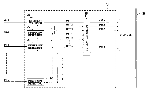
A first embodiment of the interrupt signal generating device 10 according to
the present
invention is described below with reference to Fig. 1. Input signals IN (IN-1
to IN-n) from
the sensors or detectors (such as detectors 11 to 14 in Fig. 2) are input to
corresponding
interrupt detectors 20 of the device 10. The interrupt detectors 20 can be
configured to
output a detection signal DET (DET-1 to DET-n) unconditionally whenever an
input signal
IN is received, or only when the respective input signal IN satisfies specific
conditions.
CA 02345593 2001-05-03
-6- -
The detection signals are output to an interrupt handler 15. Following
predefined conditions,
interrupt handler 15 outputs a received detection signal as an interrupt
signal INT (INT-1 to
INT-n) of a specific priority. The interrupt handler is designed such that the
priority of an
s interrupt signal corresponding to a particular input signal can be
arbitrarily set irrespective
of which of input signals IN-1 to IN-n is applied to which of the interrupt
detectors 20 and
the physical connections between interrupt detectors 20 and interrupt handler
15.
The interrupt signals INT are applied via interrupt signal line 26 to the
interrupt ports of
CPU 1. Priority is determined by CPU 1 for each interrupt port, and interrupt
processes are
run according to the port priority. It is therefore possible to select and
change the priority
with which a certain interrupt signal is processed by selecting or changing
the interrupt port
of the CPU 1 to which that interrupt signal is applied. The interrupt handler
15 and
interrupt detectors 20 receive control data from CPU 1 by way of bus line 25,
and can be
1s configured to detect interrupt events and set or change interrupt signal
priority based on the
received control data.
Fig. 4 shows a first embodiment of the interrupt handler 15. The interrupt
handler 15 of this
embodiment comprises a controller 17, a state memory 18, and a signal
distributer 19.
Detection signals DET are input to the signal distributer 19. The signal
distributer 19 may
be any device having a plurality of input and output terminals that allows
switching the
assignment between the input and output terminals. The signal distributer 19
functions as a
priority setting/changing unit.
An example of the signal distributer 19 is shown in Fig. 5. The signal
distributer 19
comprises n selectors 19-1 to 19-n. Only the first selector 19-1 is shown in
detail and will be
explained below because all selectors 19-1 to 19-n are identical in structure
and function. All
detection signals DET-1 to DET-n are applied to all selectors 19-1 to 19-n in
parallel.
Selector 19-1 has an n-stage selection register 46. Each stage holds one bit,
i.e., there is one
bit for each of the n detection signals DET-1 to DET-n. The outputs of the n
stages of
selection register 46 are applied to first inputs of AND gates Al to An,
respectively. The
detection signals are applied to respective second inputs of the AND gates. In
the example
shown, the output of the first stage and detection signal DET-1 are applied to
AND gate Al,
the output signal of the second stage and detection signal DET-2 are applied
to AND gate A2,
etc. The outputs of AND gates Al to An are applied to respective inputs of an
OR gate 47
providing the output signal of-selector 19-1, i.e., the interrupt signal INT-
1. Although not
shown in the drawings a signal formatter may follow the signal distributer as
an output
stage of the device 10, as needed, to ensure a desired format, such as pulse
width, of the
interrupt signals. This applies to all embodiments described in this text.
If the value of the bit in one of the n stages of selection register 46 is 1
and that of all other
stages is 0, only the AND gate corresponding to the 1 bit is enabled while all
other AND
gates are disabled. A 1:1 correlation between input/detection signals and
interrupt signals
can be achieved by setting the bits in the n selection registers of selectors
19-1 to 19-n so that
in each selector a different one of the n AND gates is enabled and all other
AND gates are
disabled. It will be appreciated that by shifting the respective 1 bit in all
selection registers
46 to another stage such setting can be easily changed while keeping the 1:1
assignment.
This allows to select and change for each input signal the interrupt port to
which the
so corresponding interrupt signal is applied (within the 1:1 assignment
constraint). Since
different priorities are assigned to different interrupt ports, this allows
selecting (and
CA 02345593 2001-05-03
7 - -
changing) the priority of an interrupt signal corresponding to a respective
detection signal.
In the example shown in Fig. 5, only the bit in the third stage of selection
register 46 is set to
1 in selector 19-1. AND gate A3 is, therefore, enabled and OR gate 47 outputs
1 only when
detection signal DET-3 is input. A signal is therefore output from the first
output terminal of
signal distributer 19 in response to detection signal DET-3. The output signal
from the first
output terminal is applied as interrupt signal INT-1 to the first interrupt
port of CPU 1
which is here assumed to have the highest priority among all interrupt ports.
Hence, the assignment between input terminals (or input signals) and output
terminals (or
output signals) of interrupt handler 15 can be set by pre-setting certain
binary values
(words), each including one 1 digit and (n-1) 0 digits, in the selection
registers 46 with all
these values differing from one another. The selection registers can
preferably be externally
pre-set or changed. Fig. 4 shows a configuration in which control is provided
by controller 17.
A particular control signal is sent to controller 17 from CPU 1 or an input
device such as an
operating panel to set or change the values in the selection registers 46. It
should be noted
that CPU 1 can control state memory 18 and signal distributer 19 by way of
controller 17 by
sending appropriate control data to controller 17 via bus line 25.
State memory 18 stores information that identifies the detection signal DET
when any is
received by interrupt handler 15. The CPU 1 can confirm the interrupt event
that caused an
interrupt signal during an interrupt process by reading the content of state
memory 18, and
can thus run the interrupt process appropriate to that interrupt event.
A second embodiment of the interrupt handler 15 is described next with
reference to Fig. 6.
The interrupt handler 15 of this embodiment comprises a different signal
distributer 16, a
controller 17, and a state memory 18. The controller 17 and state memory 18
are identical to
those of the first embodiment in Fig. 4, and only signal distributer 16 is
therefore described
below.
As described above, signal distributer 19 distributes n detection signals DET-
1 to DET-n to n
interrupt signals INT-1 to INT-n with a unique relationship between the
detection and
interrupt signals. By contrast, signal distributer 16 distributes n detection
signals DET-1 to
DET-n to m interrupt signals INT-1 to INT-m with m < n. In other words, signal
distributer
16 groups some or all of the n detection signals DET-1 to DET-n according to
specific
conditions into m interrupt groups and provides one interrupt signal for each
group.
Referring to only the signal distributer, its function can be defined as
grouping some or all of
its n input terminals into m groups and to assign each group to one of its m
output terminals,
a different one for each group. The conditions based on which the signals (or
input
terminals) are grouped are controlled by controller 17. As described above,
controller 17 can
be controlled by CPU 1 using bus line 25. The CPU normally has eight interrupt
ports, but
there can be more than forty input signals (and thus detection signals) that
represent
interrupt events. An appropriate interrupt process can be run even when there
are
numerous detection signals by appropriately grouping the detection signals and
assigning
interrupt signal priority by interrupt group.
Fig. 7 shows an exemplary method of grouping plural detection signals. In this
example the
priority of the interrupt processes performed by the CPU decreases in a
reciprocal relation to
the number 1 to m of the interrupt signals. A power supply error, for example,
could result in
equipment damage and disable normal operation, and is therefore normally
handled by an
interrupt process having the highest priority. In the example shown in Fig. 7,
power supply
CA 02345593 2001-05-03
-8- -
errors, reset instructions, and watchdog timer input are assigned the highest
priority. It
should be noted that while the watchdog timer signal is treated as a high
priority signal in
Fig. 7, a CPU runaway cannot occur in the sleep mode. The sleep mode
transition process
can therefore be designed to the change interrupt signal priority so that,
e.g., the priority of
the watchdog signal is lowered in the sleep mode, to that of INT-4, for
instance.
It will thus be understood that the present invention allows setting and
changing the
interrupt signal priority statically, i.e., not dependent on any operating
mode, but also
dynamically, namely in response to a change in operating mode.
The second highest priority is assigned to conditions that will cause a
problem with printing,
such as no ink cartridge, an open ink cartridge, or no paper.
Next-highest priority is assigned to such events as the operator pressing the
paper feed
button, and home position detection by a sensor. It will be obvious that the
priority assigned
to specific events will vary according to the design concept of the a
particular apparatus.
Furthermore, while events are grouped into four interrupt groups in this
example, the
specific number of interrupt groups will be determined according to need or
the number of
interrupt ports on the CPU 1.
Fig. 8 shows an exemplary configuration of signal distributer 16. In this
example, signal
distributer 16 comprises m selectors 16-1 to 16-m as opposed to n selectors in
signal
distributer 19. Selectors 16-1 to 16-m shown in Fig. 8 are substantially the
same as selectors
19-1 to 19-n in Fig. 5. Only the binary values set in selection registers 46
are different in
that, in signal distributer 16, the selection register of one or more
selectors holds a binary
value with more than one 1 digit. In order to obtain in interrupt signal in
response to each of
the n detection signals, there must be a total of n 1 bits in all selection
registers together.
How these n 1 bits are distributed among the individual selection registers
depends on how
the n detection signals are to grouped into those m interrupt groups or, in
other words,
so which detection signals are included in which interrupt group is determined
by presetting
respective values in the selection registers 46.
For example, bits 2, 3, and 4 are set to 1 in selection register 46 of first
selector 16-1 shown
in Fig. 8. AND gates A2, A3, and A4 are therefore enabled, and OR gate 47
outputs 1 when
any one of detection signals DET-2, DET-3, and DET-4 is input. As a result,
interrupt signal
INT-1 is output by first selector 16-1 when any one of three detection signals
DET-2 to DET-4
is applied.
Setting the selection registers 46 can be controlled by the controller 17 as
described above
with reference to Fig. 4. As also noted above, controller 17 can be controlled
by the CPU by
way of bus line 25. Setting the selection registers 46 can therefore also be
controlled by CPU
1 or by an external operating panel, for example.
A process for handling further detection signals that may be received while an
interrupt
process, triggered by a previous detection signal of the same interrupt group,
is being
executed, is described next with reference to Fig. 9. Fig. 9 is a function
block diagram
showing a third embodiment of interrupt handler 15 which is a modification of
the second
embodiment. In addition to the signal distributer 16, controller 17 and state
memory of the
second embodiment, the interrupt handler 15 of this third embodiment includes
an interrupt
mode register 73.
CA 02345593 2001-05-03
9
State memory 18-1 in this embodiment has a state register 71 and a history
register 72. The
state register 71 stores the fact that a certain detection signal has been
received and
information identifying each received detection signal. State register 71 and
history register
72 may each be an n-bit register, for instance, having a respective bit (flag)
for each of the n
detection signals. The contents of history register 72 is the same as that of
state register 71
as longs as the CPU 1 is in its normal operating mode, and can be read by the
CPU by way of
bus line 25 when the CPU starts running an interrupt routine. When an
interrupt routine is
triggered in any of the m interrupt groups, CPU 1 sets a corresponding mode
flag in mode
register 73 indicating that an interrupt mode was entered. This is done
separately for each of
the m interrupt groups, i.e., mode register 73 holds m such mode flags.
When an interrupt occurs, the CPU sets that mode flag in mode register 73 that
is assigned
to the interrupt group having triggered the interrupt (for easier reference
the interrupt
group having triggered a running interrupt routine will be assumed to be the
first interrupt
group). Because interrupt modes are managed separately for each interrupt
group, the
remaining mode flags remain unchanged and there is no effect on the other
interrupt groups.
When the mode flag in mode register 73 corresponding to the first interrupt
group is in the
set state, state register 71 and history register 72 are controlled by
controller 17 as follows.
When a detection signal assigned to a different interrupt (suppose: the
second) group is
received, the state register 71 is updated and the change is copied to history
register 72 as in
the normal operating mode (assuming that the mode flag for the second
interrupt group is in
the reset state). On the other hand, when a detection signal assigned to the
same interrupt
group (the first interrupt group) is received, the state register 71 is
updated but this change
is not copied to history register 72. The contents of state register 71 and
the contents of
history register 72 thus differ.
When the interrupt routine ends and CPU 1 resets the mode flag it had set
before, controller
17 is caused to compare the contents of state register 71 with that of history
register 72. If
the contents differ, a control signal is output from controller 17 to signal
distributer 16, and
a corresponding interrupt signal is sent from signal distributer 16. Another
interrupt routine
is thus performed and the same procedure is repeated. Because a separate flag
is kept for
each detection signal in state register 71 and history register 72, controller
17 knows which
detection signal has been kept waiting, when there is a mismatch between the
two registers.
Fig. 10 is a flow chart of the interrupt signal output process of this
interrupt signal
generating device and the interrupt routine of the CPU. Fig. 11 shows settings
stored in
state register 71, history register 72, and mode register 73 by way of
example. Interrupt
signal output and CPU operation are described next below with reference to the
flow chart in
Fig. 10 and Fig. 11. Note that for simplicity only four interruptsignals
corresponding to four
interrupt groups are used in the following explanation.
First, when a detection signal DET is received (S101 returns Yes), an
interrupt signal INT is
output (S102), the corresponding bit Fx (x=1,:..,n) in state register 71 is
set to 1, and this
as change in state register 71 is copied to history register 72. If detection
signal DET-3, for
example, is received in this step, bit 3 is set to 1 in both state register 71
and history register
72 as shown in Fig. 11 (a) and (b). Interrupt signal INT-1 is output to the
CPU because
detection signal DET-3 belongs to the first interrupt group assigned to
interrupt signal INT-
1 as shown in Fig. 11.
When it receives the interrupt signal (S201 returns Yes), the CPU disables the
interrupt port
CA 02345593 2001-05-03
10- -
involved (port 1) and, thereby, prohibits receiving subsequent interrupt
signals (S202). It
then sets the respective mode flag 1 (mode flag 1, the mode flag assigned to
the first
interrupt group, in this example) in the mode register 73 of that interrupt
signal generating
device 10 that sent the interrupt signal (S203), reads the contents of history
register 72
(S204) to confirm the interrupt event, and runs the corresponding interrupt
process (S205,
S206).
The device 10 monitors the mode register. When it detects that mode flag 1 in
mode register
73 is set to 1 as shown in Fig. 11 (c) (S104), controller 17 restricts
updating the history
register 72, i.e., it does not copy any further change in bits 1 to 5 in state
register 71 to the
history register 72 (S106). That is, even if any of detection signals DET-1 to
DET-5 associated
with the same (i.e., the first in this example) interrupt group is received,
the corresponding
update in bits 1 to 5 is not copied to history register 72.
If another detection signal is received during an interrupt routine (S107
returns Yes), and
the detection signal belongs to an interrupt group other than The first
interrupt group, steps
S102 to S107 and CPU steps S201 to S206 are repeated. If the detection signals
belongs to
the same, i.e. the first, interrupt group, only steps S102 to S107 are
repeated. In this latter
case however, because an interrupt routine is already in progress, only state
register 71 is
updated whereas updating of history register 72 is restricted. Therefore,
assuming for
example that detection signal DET- 1 is received, bits 1 and 3 in state
register 71 are set to 1
as shown in Fig. 11 (d), but history register 72 remains with only bit 3 set
to 1 as shown in
Fig. 11 (b). In this latter case, interrupt signal INT-1 is output to the CPU
in step S102, but
it has no effect because the CPU's interrupt port 1 is disabled. This is
because running two
interrupt routines of the same level at the same time would require a complex
control. It
should be noted, however, that whereas the flow chart in Fig. 10 describes a
configuration
that outputs another interrupt signal of the same number even when the same
detection
signal is again generated during an interrupt routine, it is also possible to
have the
configuration so that such repeated output of the same interrupt signal while
the interrupt
routine triggered by the first occurrence of that interrupt signal is still
being executed, is
prevented. This is described further below.
When the CPU interrupt process ends (S206 returns Yes), the CPU clears the
interrupt
mode, i.e., it resets mode flag 1 in our example (S207), enables the interrupt
port (port 1)
3s (S208), and ends the interrupt routine.
When controller 17 in the device 10 notices that the mode flag is reset, it
compares the
contents of state register 71 with that of history register 72 (S109). If the
contents are the
same (S110 returns Yes), registers 71 and 72 are reset or only state register
71 is reset, the
update restriction of history register 72 is canceled and the process ends.
Note that this reset
of registers 71 and 72 or only register 71 concerns only the bits assigned to
the interrupt
group that triggered the interrupt process that was completed in step S206.
Note further
that resetting of only register 71- would be sufficient because the update of
history register
72 in response to the next detection signal from the same interrupt group will
harmonize the
bit values of both registers corresponding to that interrupt group Because
detection signal
DET-1 is received during the interrupt routine in this example, the contents
of state register
71 and that of history register 72 differ as shown in Fig. 11 (b) and (d) and
step S110 thus
returns No. When S110 returns No, control loops back to step S102, interrupt
signal INT-1
corresponding to detection signal DET-1 is output, and the process described
above (steps
S102 to S11l) is repeated. The CPU can perform the appropriate interrupt
process (steps
S201 to S208) because the interrupt port 1 has been enabled again as described
above.
CA 02345593 2001-05-03
-11-
Fig. 12 is a function block diagram of a fourth embodiment of the interrupt
handler 15. This
embodiment is adapted to block repeated interrupt signals of the same
interrupt group
during an interrupt routine triggered by a previous interrupt signal from that
interrupt
group. To achieve this additional function, an interrupt output controller 75
is added to the
signal distributer 16. Although interrupt output controller 75 is shown
external to the signal
distributer 16 in the configuration shown in Fig. 12 for easier understanding
of the
configuration of the controller 75 it may in fact be part of the signal
distributer 16. The
example shown in Fig. 12 is also described using only four interrupt signals
INT-1 to INT-4.
ia
While only one pair of AND gate 76 and inverter 77 is shown in Fig. 12,
controller 75 is in
fact assumed to have four such pairs, one for each pair of AND gate (Bi to B4)
and OR gate
(C1 to C4); the output terminals 1- 4 of the mode register 73 are separately
connected to the
respective AND gate 76 and inverter 77 of each pair. Furthermore, controller
17 outputs the
result of comparing the contents of state register 71 with that of history
register 72 on line
74, which is commonly connected to all AND gates 76.
An output terminal of mode register 73 goes high (= 1) when the corresponding
mode flag is
set as explained above. Let us assume output terminal 1 of mode register 73
goes high. This
causes inverter 77 to disable AND gate B1 for interrupt signal INT-1, so that
the output of
interrupt signal INT-1 is disabled by AND gate Bl until the mode flag is
reset.
When controller 17 detects that the mode flag has been reset, it compares the
contents of
state register 71 with that of history register 72 and sets line 74 high if
the contents differ.
At this stage mode register 73 is not cleared and output terminal 1 stays
high. As a result,
the inputs of the AND gate 76 connected to output terminal 1 of mode register
73 meet the
AND condition. As a result, one input to OR gate Cl corresponding to the
output terminal of
the mode register 73 goes high, and interrupt signal INT-1 is output. The
controller 17 can
then either clear the mode flag 1 in mode register 73 or the mode register 73
can hold the
mode flag. If the comparison of registers 71 and 72 detects a match, mode
register 73 is
cleared. Incidentally, if a signal formatter as mentioned above is to be used
with this
embodiment it could be arranged to be in between signal distributer 16 and
controller 75 or,
more preferably, it could be arranged to follow controller 75.
Embodiments of the interrupt detectors 20 in the interrupt signal generating
device 10
according to the present invention are described below. Although each of the
embodiments of
the interrupt handler 15 described above can be combined with each of the
embodiments of
the interrupt detectors to be described below, the following description uses
the interrupt
handler 15 shown in Fig. 6 as an example.
Fig. 13 is a function block diagram showing a first embodiment of an interrupt
detector 20
for use in a device 10 according to the present invention. The interrupt
signal generating
device 10 has a total n interrupt detectors 20 corresponding to n input
signals IN-1 to IN-n.
Fig. 13 shows the internal configuration of only one of the interrupt
detectors 20, namely
that for input signal IN-1, because each of the n interrupt detectors 20 can
have the same
structure. A case where individual ones of the n interrupt detectors may have
different
structures is explained later.
In this first embodiment, the interrupt detector 20 has a pattern generator
21, a pattern
comparator 22, and a detection signal generator 23. The pattern generator 21
generates a
CA 02345593 2001-05-03
-12- -
specific signal pattern from the input signal as will be explained in more
detail later. Signal
pattern generation by the pattern generator 21 is controlled according to
conditions set by
the CPU by way of bus line 25. The signal pattern generated by pattern
generator 21 is
output to pattern comparator 22.
Pattern comparator 22 compares the signal pattern received from the pattern
generator 21
with a reference pattern. The data representing this reference pattern is sent
from the CPU
1 by way of bus line 25. If the pattern comparison detects a match between the
signal pattern
and the reference pattern, a match signal is output to both detection signal
generator 23 and
state memory register 18. As will be explained in more detail later, this
pattern comparison
may be regarded as a kind of filtering whose main purpose is to pass relevant
input signals
as detection signals but to block irrelevant input signals such as noise. In
absence of this
filtering noise, for instance, could be mistaken as an input signal. In this
sense, a match
signal is an input signal that has passed the filter.
The state memory register 18 stores for each of the n interrupt detectors a
respective flag (a
bit) that is set in response to the match signal. The CPU 1 can identify the
interrupt event
and confirm the apparatus status, such as what error occurred, by reading the
contents of
this state memory register 18 in the routine performed after the interrupt
occurs.
Detection signal generator 23 checks whether to send a detection signal to the
interrupt
handler 15 when it receives a match signal. More specifically, the detection
signal is not
output immediately when a match signal is received, but is output only when
specific
conditions are met. The intention is to have the sleep mode, if any, continue
even when for
any of the input signals IN-1 to IN-n a match signal is received unless other
conditions are
also met. When no detection signal is output, no interrupt signal is applied
to CPU 1, but the
fact of the match signal having been output is stored in state memory register
18. It is
therefore possible for CPU 1 to confirm, when a subsequent interrupt occurs,
that there is an
unprocessed match signal and to perform a process appropriate to the error.
The conditions
under which interrupt detector 20 generates a detection signal in response to
a match signal
can be set by CPU 1 via bus line 25 and can be freely determined in accordance
with the
design concept of the particular electronic apparatus.
As described above, the CPU 1 can thus freely set the conditions for
generating a signal
pattern from an input signal, set the reference pattern, and set the
conditions for generating
a detection signal. It is therefore possible to accomplish an interrupt
process that is
appropriate with respect to complicated conditions and differences in the time
scale of state
changes according to the diverse actual operating environments in which the
apparatus may
be used.
Fig. 14 shows a more detailed example of this first embodiment of the
interrupt detector 20
and will be used to explain one way of pattern generation and comparison. As
shown in Fig.
14, pattern generator 21 has a clock selector 31 and a shift register 30,
pattern comparator
comprises a comparator 22a and a pattern memory 22b storing the reference
pattern, and
detection signal generator 23 includes a state change detector 23a and an
interrupt settings
register 23b.
A frequency divider 37 frequency-divides an input clock into plural clocks of
different
frequencies that are input to clock selector 31, which selects one of the
applied clocks based
on output from a clock selection data storage 32. By thus selecting a
particular clock from
among plural clocks, the clock frequency appropriate to an event to be
detected can be used
CA 02345593 2001-05-03
-13-
to generate a signal pattern. Different clocks may be selected for different
ones of the n
interrupt detectors 20.
Which clock, i.e., which frequency, is used is preset by CPU 1 in clock
selection data storage
32, and can be changed as necessary by CPU 1. Furthermore, frequency divider
37 is
disposed externally to interrupt detectors 20 so that the plural clocks can be
supplied to all
interrupt detectors 20 by providing one frequency divider 37 common to input
signals IN-i to
IN-n.
Input signal IN-1 is applied to shift register 30, which is clocked by the
clock selected as
explained above. The input stage of shift register 30 samples input signal IN-
1 and the
contents of the whole shift register is sequentially shifted with each clock
pulse. Although a
4-stage shift register is shown in Fig. 14, more or fewer stages can be used
as needed. The
output signals from all the shift register stages are output as a signal
pattern to comparator
22a.
~
Comparator 22a compares the reference pattern previously stored in the pattern
memory
22b with the signal pattern output from shift register 30, and outputs a match
signal to state
memory register 18 and detection signal generator 23 when a match is detected.
The state
change detector 23a outputs a detection signal when conditions stored in
interrupt settings
register 23b are met. CPU 1 controls storing these conditions to interrupt
settings register
23b by way of bus line 25.
Fig. 15 is a timing chart showing the (selected) clock, input signal IN-1, the
output signals of
the four shift register stages and the match signal. Note that the reference
pattern stored in
this example is 1110.
Let us assume that input signal IN-1 goes high at the timing shown in Fig. 15,
i.e., within
the pulse width of a clock pulse numbered 0. Note further, that the shift
register 30 is
supposed to be edge triggered and thus sequentially shifts its contents at
each rising edge of
the clock. Because input signal IN-1 is low at the rising edge of clock pulse
0, shift register
30 cannot detect a change in the input signal. Shift register 30 therefore
outputs 0000 at this
time.
Stage 1 of shift register 30 goes high at the rising edge of clock pulse 1,
the next clock pulse,
because input signal IN-1 is high. The signal pattern output by shift register
30 is therefore
1000 at this time. -
Input signal 1 is high at the rising edge of clock pulse 2, stage 1 therefore
remains high and
stage 2 goes high resulting in a signal pattern 1100.
In the same way, shift register 30 outputs signal pattern 1110 at clock pulse
3. This signal
pattern matches the reference pattern 1110, and the match signal therefore
goes high at the
timing of a sampling signal also shown in Fig. 15.
Shift register 30 outputs signal pattern 1111 at clock pulse 4. This does not
match the
reference pattern 1110, and the match signal output therefore stops. This
configuration
achieves the following benefits.
First, improper operation as a result of noise can be prevented because a
match signal is not
output unless there is no signal input for a specific continuous period of
time. Furthermore,
CA 02345593 2001-05-03
-14- -
when a match signal is output only when there is a match with the reference
pattern 1110
(or another reference pattern different form Illl), the match signal is output
only for as long
as there is a pattern match even if the input signal continues for an extended
period, and
continuous interrupt signal output can thus be prevented.
It is also possible, however, to continue outputting a match signal even if a
match is no
longer detected, when it is desirable to control interrupt signal generation
under other
conditions. This may be achieved by storing the match signal from comparator
22a in a latch,
flip-flop or other device in the detection signal generator 23 and using the
output signal from
that device as the match signal.
Alternatively, the match signal can be held by setting the reference pattern
to 1111. In this
case, match signal output continues for as long as the respective input signal
is high once all
shift register stages went high as shown in the bottom row in Fig. 15. When
the reference
pattern is set to 1111 and the match signal is output continuously, match
signal output stops
automatically when the respective input signal is no longer present (is low).
This
configuration thus provides the additional benefit of not requiring a reset
operation such as
would be required when a latch or similar device is used as noted above.
The pattern match detection explained above can also be used to let the host
50 cause the
CPU 1 to change from a sleep mode to the normal operating mode. This is
further described
with reference to Fig. 16 showing a function block diagram of the related
configuration.
Fig. 16 shows host 50 and a communication terminal 60 (such as the printer of
Fig. 2)
connected to it. This communication terminal 60 has an interrupt signal
generating device
10 according to the present invention including n interrupt detectors 20 as
described before.
One of these n interrupt detectors has the structure as shown in Fig. 14 and
is reserved for
use by the host to wake up the CPU. Different from the remaining n-1 interrupt
detectors,
this one does not receive an input signal from any sensor or detector. The
remaining n-i
interrupt detectors may but need not necessarily have the structure of Fig.
14. To simplify
and make it easier to understand the essential points of the following
explanation, the
detailed configuration of communication terminal 60 is not shown in Fig. 16.
Note, further,
that 1110 is stored as reference pattern in the pattern memory 22b of the
interrupt detector
20.
When host 50 wants to change CPU 1 of communication termina160 to the normal
operating
mode, host 50 sends a 1110 bit pattern to communication terminal 60. Level
converter 27,
protocol converter 28 and device 10 of communication terminal 60 continue
operating even
when CPU 1 is in the sleep mode. The 1110 bit pattern sent from host 50 is
therefore
received, passed through level converter 27 and protocol converter 28, and
input into shift
register 30 of interrupt detector 20.
Because a reference pattern 1110 is stored in pattern memory 22b, a match
signal is output
from the comparator 22a. As a result, detection signal generator 23 outputs a
detection
signal to interrupt handler 15. Based on this detection signal, interrupt
handler 15
generates an interrupt signal and sends it to the corresponding interrupt port
of CPU 1. The
interrupt signal then causes CPU 1 to change from the sleep mode to an
operating mode. The
CPU 1 having returned to the normal operating mode reads the state memory 18
and will
learn from the information found therein that not any critical error occurred
but the host 50
so is asking for attention.
CA 02345593 2001-05-03
15-
It will be understood by those skilled in the art that various means can be
used to write the
1110 bit pattern from host 50 to shift register 30. Typical methods use a
serial interface or a
parallel interface. Using a serial interface is described first. The received
data is output from
protocol converter 28 as serial data, synchronized to a specific clock, to
shift register 30 and
entered into the shift register 30 with the register's shift clock as applied
by clock selector 31.
Clock selector 31 selects, as the shift clock, a clock that is synchronized to
the serial data
synchronization clock (not shown in the figure). If a parallel interface is
used, the received
data 1110, for example, can be directly input to the shift register 30 as
parallel data.
A second embodiment of an interrupt detector for a device according to the
present invention
is described next with reference to Fig. 17. Fig. 17 is a function block
diagram of an interrupt
detector 20 according to this embodiment.
The difference between the interrupt detector shown in Fig. 17 and that shown
in Fig. 15 is
is that the former has a presettable frequency divider 38 between clock
selector 31 and shift
register 30. This configuration makes it possible to reduce the frequency
(increase the
period) of the clock input to the shift register 30 by any desired factor 1/N.
The value of N
(being an integer) is stored in a divisor memory 39 and is preset into the
frequency divider
38. The CPU 1 can set and change the value N stored in divisor memory 39 as
required. The
w frequency divider 38 is provided in addition to the frequency divider 37 to
increase the
flexibility regarding the available shift clock frequencies. Cases where such
increased
flexibility is useful will be explained in the context of the next embodiment.
A third embodiment of an interrupt detector for use in a device 10 according
to the present
zs invention is described next with reference to Fig. 18. Fig. 18 is a
function block diagram of
an interrupt detector 20 which can be viewed as a modification of the first or
the second
embodiment. It will be noted that parts of this interrupt detector 20 not
shown in Fig. 18 are
the same as corresponding parts in the previously described embodiments. This
interrupt
detector 20 adds to the previous embodiments a match count unit 40 including a
16-bit
30 counter 41, a count comparator 42, and a count memory 43.
In this embodiment the match signal from comparator 22a is input to the enable
terminal En
and clear terminal CLR of counter 41. Counting thus continues for as long as
the match
signal is output, but the counter is reset when the match signal disappears
and resumes
35 counting when the next match signal is output. This configuration is
effective when it is
required to determine if the match signal is continuously output for an
extended time
exceeding a threshold limit. It should be noted that while a 16-bit counter 41
is used in this
embodiment, a counter using more or less than 16 bits can be used as needed.
40 The count comparator 42 compares the count value of counter 41 with the
value preset into
count memory 43 by CPU 1. If the two values match, a detection signal is
output to interrupt
handler 15. Based on this detection signal, interrupt handler 15 generates an
interrupt
signal of a specific priority, and. sends the resulting interrupt signal to
the respective
interrupt port of CPU 1. The CPU is activated when an interrupt signal is
applied to the
45 interrupt port, and thus confirms the interrupt event and runs the required
appropriate
process as controlled by the interrupt routine stored in ROM 8 or RAM 9.
Interrupt detector 20 according to this third embodiment is effective when an
interrupt
signal is generated on the condition that an input signal IN longer than a
normal signal is
so present. The number of stages in the shift register 30 would have to be
increased if the
presence of a long input signal were to be detected using a clock with a
relatively short
CA 02345593 2001-05-03
-16- -
period. On the other hand, input signals to the pattern generator 21 cannot be
uniformly
increased in length because a wide range of input signals IN is possible. For
example, there
could be a difference of more than 1000 times in the period of signals that
must be detected
as interrupt events (the period could be only 20 gs in a short signal, and 20
ms or longer in a
long signal).
If the length of input signals to be detected can be as long as 1000 times the
shortest
detected signal, it is not only impractical for frequency divider 37 to
generate clocks of each
corresponding frequency, it is also not possible to generate accurate signal
patterns. The
shift register 30 samples the input signal at the rising edge (which could
alternatively be the
falling edge) of the shift clock. Therefore, if an input signal disappears
during one shift clock
period but is present again at the next rising edge, the input signal is
sequentially shifted as
though nothing had happened, and the input signal change cannot be detected.
The possibility that such problems occur increases as the period of the shift
clock becomes
longer, and it is therefore not desirable for the shift clock period to be
very long. This also
applies when the clock period is increased by frequency divider 38 in the
interrupt detector
20. If a shift clock with a short period is used to avoid such problems, the
shift register 30 of
pattern generator 21 needs an extremely large number of shift stages in order
to generate
the signal pattern for a long input signal.
Different types of interrupt detectors 20 can be used for input signals of
different lengths.
For example, an interrupt detector according to the first or second embodiment
is used for
interrupt detection of input signals of a typical common length, and an
interrupt detector
according to the third embodiment is used for interrupt detection of input
signals
particularly longer than these other input signals.
The detection signal output timing of the interrupt detector 20 shown in Fig.
18 is described
next with reference to the timing chart in Fig. 19.
In this example 16-bit counter 41 counts clock pulses of a clock B shown in
the uppermost
row in Fig. 19. The period of this clock is typically longer than that of the
clock A applied to
shift register 30 in order to detect particularly long input signals. When the
match signal
goes from low to high, enable terminal En of counter 41 goes high and counting
begins.
When counter 41 reaches a count equal to the count stored in count memory 43,
a count
match signal is output. This count match signal can be applied to detection
signal generator
23 instead of the match signal from comparator 22a, or it can be directly used
as a detection
signal.
The counter 41 is cleared (bottom row in Fig. 19) and no count match signal is
output if
comparator stops outputting the match signal before the counter 41 has counted
the stored
count value (indicated by dotted lines). A detection signal is therefore not
output, and an
interrupt does not occur when the match signal from comparator 22a is shorter
than the
period required for counter 41 to reach the count value stored in count memory
43.