Note: Descriptions are shown in the official language in which they were submitted.
CA 02345605 2001-04-30
-1-
METHOD OF TESTING EMBEDDED MEMORY ARRAY AND
EMBEDDED MEMORY TEST CONTROLLER FOR USE THEREWITH
[ 0001 ] The present invention relates, in general, to testing of memory
arrays
and, more specifically, to a method of efficiently repeating test instructions
and to a
test controller for use therewith.
BACKGROUND OF THE INVENTION
[ 0002 ] Memory BIST controllers use a very wide instruction word (e.g., 40
bits) for programming algorithms. A memory test developer may specify as many
instructions as required in a memory BIST microprogram memory array to perform
a
memory test. However, since the developer wishes to keep the number of gates
required to implernent a word in the memory array to a minimum, it is
desirable to
keep the number of instructions to a minimum. Generally, each word requires
about
250 gates.
[ 0003 ] Many memory test algorithms, particularly March algorithms,
repeatedly perform the same operations but with opposite data or parameters or
traverse an address space in one direction and then in the opposite direction.
The
conventional way of doing this utilizes many more instructions than are
required.
This requires many more gates than required.
0004 ] Kalter et al United States Patent No. 5,961,653 granted on October 5,
1999 for "Processor based BIST for an embedded memory" describes a processor
based BIST macro for testing memory embedded in logic and includes a base ROM
which is structured to have test instructions written into it in microcode
form. The
base ROM component is configured having 160 addresses by 34 bits wide,
providing
for a total of 160 test instructions, branch statements to be used in
conjunction with
the instructions and a scannable ROM. The scannable ROM is configured having
34
addresses by 34 bits wide. The arrangement allows for altering, adding,
deleting,
changing the sequence of any test patterns and looping within a single pattern
or
any group of patterns. The 34 address lines in the scannable ROM allow for 17
branch instructions which bound the beginning and end of each test pattern
produced from the base ROM and 17 extra instruction words to accommodate any
modifications or changes. The scannable ROM addresses are typically sequenced
from 192 through 225. The two ROMs and are multiplexed together onto a 34 bit
test buss controlled by the sequencer.
CA 02345605 2001-04-30
-2-
[ 0005 ] Illes et al United States Patent 5,925,145 granted on July 20, 1999,
for "Integrated circuit Tester with Cached Vector Memories" discloses an
integrated
circuit tester which includes a set of nodes providing test access to separate
terminals of an IC and each carrying out a sequence of actions at the terminal
in
response to test vector sequences. Each node includes a low speed vector
memory
supplying test vectors during the test. A host writes vectors into the vector
memories
before the test sending them over a common bus to vector write caches within
each
node which compensate for access speed limitations of the vector memory.
During
the test, blocks of vectors are read out of the vector memory at a low rate
and written
into a high speed read cache array. An instruction processor within each node
reads
individual vectors read out of the read cache array at a high rate and uses
them for
controlling test operations at the node during each cycle of the test. The
read cache
array also allows the instruction processor to re-use repeated vector
patterns,
thereby reducing the number of vectors that must be distributed to the nodes.
. [ 0006 ] Ozawa et al. United States Patent 6,038,649 granted on March 14,
2000 for "Address Generating Circuit for Block Repeat Addressing for a
Pipelined
Processor" discloses an address generating circuit for repeating a selected
block of
instructions. An instruction address maintained by a program counter is
compared to
register that holds the address of the end of the selected block of
instructions.
When the end address is detected, the program counter is loaded with a
starting
address of the block of instructions. A Block repeat count register maintains
a
repeat count. A zero detection circuit delays decrements by a number of clock
cycles
that is equivalent to a pipeline depth for instruction prefetching of a
processor
connected to the program counter. The zero detection circuit outputs a loop-
end
control signal which controls a selector to selectively provide an incremented
address or the start address to the program counter. By delaying decrements,
the
state of the repeat count is correctly maintained when the processor pipeline
is
flushed during an interrupt. The zero detection circuit also deactivates the
loop-end
control signal for the number of clock cycles equivalent to the depth of the
pre-fetch
pipeline during the final repeat loop iterations) so that a loop with a block
size less
than or equal to the depth of the prefetch pipeline can be repeated the
correct
number of times.
0007 ] Heidel et al United States Patent 6,108,798, granted on August 22,
2000 for "Self programmed built in self test, discloses a Dynamic Random
Access
Memory (DRAM) with self-programmable Built In Self Test (BIST). The DRAM
CA 02345605 2001-04-30
-3-
includes a DRAM core, a Microcode or Initial Command ROM, a BIST Engine, a
Command Register and a Self-Program Circuit. During self test, the BIST engine
may test the DRAM normally until an error is encountered. When an error is
encountered, the Self-Program Circuit restarts the self test procedure at less
stringent conditions.
SUMMARY OF THE INVENTION
( 0008 ] The present invention provides a method for repeating an instruction
or a series of consecutively executed instructions with modifications to the
instruction
fields of each commands as well as a circuit especially adapted to carry out
the
method.
( 0009 ] One aspect of the invention is generally defined as a method for
testing memory embedded in an integrated circuit, the method comprising
executing
each instruction of a plurality of test instructions in sequence, each
instruction having
an inactive repeat control field except for a last instruction of each of one
or more
groups of one or more instructions to be repeated, each of the last
instruction having
an active repeat control field; and, for each instruction having an active
repeat
control field, executing, in sequence, the instructions of the group of
instructions with
which each instruction is associated for a predetermined number of repeat
cycles for
2o the group; and, for each repeat cycle, modifying predetermined fields of
each
instruction in accordance with a predetermined field modification instructions
for
each repeat cycle.
( 0010 ] Another aspect of the invention is generally defined as an memory
improvement to a test controller for testing a memory array, the controller
having a
test instruction register array having registers for storing a plurality of
test
instructions, each register having instruction fields for storing memory
addressing
sequencing data, write data sequencing data, expect data sequencing data and
operation data specifying an operation to be performed on the memory array,
the
improvement comprising a repeat module for repeating a group of one or more
test
instructions with modified data, the repeat module including storage means for
storing instruction field modification data; and each register of the test
instruction
register array including an instruction field for enabling or disabling the
repeat
module.
( 0011 ] A still further aspect of the present invention is generally defined
as a
test controller for use in testing memory imbedded in an integrated circuit,
the test
CA 02345605 2001-04-30
-4-
controller comprising a scannable microcode register array having one or more
instruction registers for storing a plurality of test instructions for
performing a test of
the memory in accordance with a predetermined test algorithm; a pointer
controller
for selecting one of the test instructions for execution and determining a
next
instruction for execution in accordance with conditions stored in each the
test
instruction; an instruction repeat module for reading address sequencing,
write data
sequencing, expect data sequencing data from a current test instruction and
outputting address sequencing, write data sequencing, expect data sequencing
data,
the repeat module being responsive to instruction repeat data in the current
test
instruction for repeating an operation specified in the test instruction with
different
data; a sequencer responsive to an operation code in the current instruction
for
performing a predetermined operation on the memory under test; and an address
generator and a data generator responsive to the output address sequencing,
write
data sequencing, expect data sequencing data for application to a memory under
test in accordance with an operation specified in the current instruction.
BRIEF DESCRIPTION OF THE DRAWINGS
[ 0012 ] These and other features of the invention will become more apparent
from the following description in which reference is made to the appended
drawings
in which:
[ 0013 ] Figure 1 is a block diagram view of a portion of a memory test
controller including a Repeat Loop microcircuit according to an embodiment of
the
present invention;
[ 0014 ] Figure 2 is a flow diagram partially illustrating the operation of a
pointer controller according to an embodiment of the present invention;
[ 0015 ] Figure 3 is a block diagram illustrating salient portions of a
pointer
controller and a scannable microcode memory array according to an embodiment
of
the present invention;
0016 ] Figure 4 is a block diagrammatic view of a repeat loop module
according to an embodiment of the present invention;
[ 0017 ] Figure 5 is a diagrammatic view of a repeat loop sub-circuit
according
to an embodiment of the present invention;
( 0018 ] Figure 6 is a diagrammatic view of a repeat trigger sub-circuit
according to an embodiment of the present invention;
CA 02345605 2001-04-30
-5-
[ 0019 ] Figure 7 is a circuit diagram of a repeat register data processing
sub-circuit according to an embodiment of the present invention;
[ 0020 ] Figure 8 is a circuit diagram of a repeat loop instruction field
modification sub-circuit according to an embodiment of the present invention;
[ 0021 ] Figure 9 is a circuit diagram of an InhibitDataCompare modification
circuit according to an embodiment of the present invention; and
0022 ] Figure 10 is a circuit diagram of an InhibitLastAddressCount
modification circuit according to an embodiment of the present invention.
DETAILED DESCRIPTION
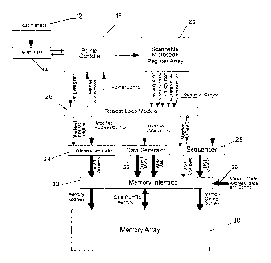
0023 ] Figure 1 is a block diagram of portion of a memory test controller 10
according to a preferred embodiment of the present invention in which the test
controller is embedded in an integrated circuit. The circuit includes a test
interface 12 for loading test instructions and data into the circuit, a Finite
State
Machine (FSM) 14 which controls the initialization, setup, and initiation of a
memory
test, a pointer controller 16 which controls the sequencing of test
instructions, and a
scannable microcode register array 20 for storing a plurality of test
instructions, as
discussed more fully below. The test controller further includes a data
generator 22
and an address generator 24 which operate to execute data and address commands
in response to data fields in an active or current microcode instruction which
has
been loaded for execution, as explained below. A repeat loop module 26 reads
the
instruction fields of the current instruction and generates memory address and
data
control signals which are applied to the data generator and address generator.
Address generator 24 controls the sequencing of the addresses applied to the
memory under test. Data generator 22 provides a programmable write data
register
(not shown) and a programmable expect data register (not shown). A number of
operations can be performed at runtime on these registers to generate a custom
data pattern. The write data register controls the data pattern written to the
memory
under test. The expect data register controls the expected data pattern used
to
compare with data read from the memory under test. The data and address
generators operate independently and are controlled by respective fields of
the
active microprogram instruction. A sequencer 28 is responsive to an operation
field
contained in a current test instruction for performing a specified one of a
plurality of
predetermined operations on the memory under test. Memory address, control
signals and data are applied to the memory under test 30 via a memory
interface 32
CA 02345605 2001-04-30
-6-
which also observes data from the memory under test. In normal operational
mode
of the circuit, address, data and control signals are applied to the memory
interface
via inputs generally designated by arrow 36. Data generators, address
generators,
sequencers and memory interfaces are well known in the art and, accordingly,
are
not described in detail herein.
Scannable Microcode Register Array
0024 J Scannable microcode register array 20 is comprised of a plurality of
serially connected instruction shift-registers. For purposes of illustration,
seven
registers are shown in Figure 3. The number of instructions in the array
depends on
the specific design requirements and design budget. Each register may be in
the
order of 34 or more bits and stores a microcode test instruction for
execution. The
instructions are "ordered" which means that the instructions are executed in
sequence. The first address is instruction zero. The instructions stored in
the
registers perform tests of the memory according to predetermined test
algorithms
under the control of the pointer controller and the repeat loop module and in
accordance with command fields contained in the instructions. An objective of
the
invention is to enable one to scan in instructions to perform memory tests
according
to virtually any test algorithm. Thus, the details of the algorithm and of the
manner in
which data pattern and address sequencing is achieved is not important for the
purposes of the present invention and, accordingly, are not described herein.
( 0025 J Test instructions are serially loaded into the scannable microcode
register array 16 via test interface 12. One instruction is executed for each
execution of an operation applied to the memory under test by the sequences.
The
microcode instructions of the memory BIST controller provide parallel control
of
blocks such as the address generator, data generator, sequences and pointer
controller, creating a wide but very flexible architecture for the generation
of complex
test algorithms. The contents of the test instructions in the scannable
microcode
register array are not modified during a test. The pointer controller,
described in
more detail later, operates to select an instruction for execution and
determines the
branch for execution of the next instruction from data contained in each test
instruction. Before describing the structure and operation of the various sub-
circuits
of the test controller, it would be useful to briefly describe the various
instruction
fields which comprise a microcode instruction. It is to be understood at the
outset
that additional fields may be provided without departing from the present
invention.
CA 02345605 2001-04-30
d
-7-
Microcode Instruction Field Descriptions
[ 0026 ] Each instruction includes at least the following instruction fields:
Address sequencing commands, including Z, X1, X0, Y1, YO address segment
fields
(referred to as Z Address Cmd, X1 Address Cmd, XO Address Cmd,
Y1 Address Cmd, YO Address Cmd, respectively, later in the description);
OperationSelect; InhibitLastAddressCount; InhibitDataCompare; WriteDataCmd;
ExpectDataCmd; BranchTolnstruction; and RepeatLoopControl and
NextConditions.
[ 0027 ] Each instruction provides a 2-bit instruction field for each of a Z
bank
address segment control field, X1 and XO row address segment control fields
and Y1
and YO column address segment control fields for the memory under test. TABLE
I
shows the address segment control field decodes which apply to all of these
fields.
Actions such as increment or decrement can be performed on each address
segment independently. The decodes are arranged in pairs so that a command can
be changed to its opposite or complement value simply reversing the least
significant
bit.
TABLE
I
0 Address
Segment
Control
Field
Decode
Field Instruction Description
Value
00 Hold
01 Hold I
10 Increment
11 Decrement
[ 0028 ] The InhibitLastAddressCount field is a single bit field which, when
active, prevents an address counter from counting the next address on a True
NextConditions.
[ 0029 J The WriteDataCmd control field is a 3-bit field which is decoded to
select the data or perform an operation on a data register which is applied to
the
memory for a write operation. It will be noted that the decodes are arranged
in pairs
in which the only difference between the bit values of members of the pairs is
the
CA 02345605 2001-04-30
8
values of the least significant bit. The repeat loop module uses this
characteristic in
a manner explained later. The field decode is shown in TABLE III.
TABLE
III
WriteDataCmd
Instruction
Field
Decode
Field Instruction Description
Value
000 Select the WriteData Register
001 Select the WriteData Register and Invert
r--
010 Select the register containing all zeroes
011 Select the register containing all ones
100 Select and Rotate the WriteData Register
101 Select and Rotate the WriteData Register
and Invert
110 Select and Rotate the WriteData Register
with Inverted
feedback
111 Select and Rotate the WriteData Resister
with Inverted
feedback and Invert i
[ 0030 ] The ExpectDataCmd instruction field is a 3-bit field which is decoded
to select the expect data or to perform an operation on an expect data
register for
comparison on a read operation. The ExpectDataCmd field decodes are identical
to
the WriteDataCmd field and are shown in TABLE IV.
CA 02345605 2001-04-30
_g_
TABLE IV
ExpectDataCmd
Instruction
Field
Decode
Field Instruction Description
Value
000 Select the ExpectData Register
001 Select the ExpectData Register and Invert
010 Select the register containing all zeroes
011 Select the register containing all ones
100 Select and Rotate the ExpectData Register
I
101 Select and Rotate the ExpectData Register
and Invert
110 Select and Rotate the ExpectData Register
with Inverted
feedback
111 Select and Rotate the ExpectData Resister
with Inverted
feedback and Invert
[ 0031 ] The InhibitDataCompare field is a single-bit instruction field which,
when set, disables any StrobeDataOut signal during execution of the specified
operation. When not set, normal comparison of expected data and read data from
the memory under test is performed.
[ 0032 ] The OperationSelect field specifies the operation to be applied to
the
memory under test. The length of the OperationSelect field is dependant on the
number of operations defined by the test algorithm designer. This field is
applied to
and used by the sequencer which is designed to perform all of the desired
operations.
[ 0033 ] The BranchTolnstruction field identifies the instruction which the
pointer control selects as the next instruction for execution if any of the
requested
NextConditions triggers, apart from the RepeatLoopDone condition, are not
true.
[ 0034 ] The RepeatLoopControl instruction field is a 2-bit field with an
instruction decode given below. As explained more fully later, the repeat loop
module
includes two 2-bit counters. As indicated in the RepeatLoopControl field
decodes
shown in TABLE II, each counter can be incremented separately or the two
counters
may be chained together to form one 4-bit counter and incremented
sequentially.
Thus, the instruction decode from the RepeatLoopControl field defines the
counter
configuration. The RepeatLoopDone condition, described below, is always
required
to increment a repeat operation if the instruction decode from the
CA 02345605 2001-04-30
a
-10-
RepeatLoopControl field is increment Loop Counter A, Increment Loop Counter B,
or
Increment Loop Counter BA.
TABLE
II
RepeatLoopControl
Field
Decode
Field Instruction Description
Value
00 Idle
01 Increment Loop Counter
A
10 Increment Loop Counter
B
11 Increment Loop Counter
BA I
[ 0035 ] The NextConditions instruction field defines the conditions which
must
test true to advance to the next instruction. The next instruction is the next
sequential instruction in the scannable microcode register array. The
conditions in
the NextConditions field include the following conditions: Z Endcount;
YO Endcount; Y1_Endcount; XO Endcount; X1_Endcount; and RepeatLoopDone.
Each of these conditions is briefly described below. An unconditional
NextConditions
is implied when all of the bits of the NextConditions field are set to zero.
The
NextConditions conditions are as follows:
[ 0036 ] the Z Endcount condition specifies whether the Z_Endcount trigger is
a required condition for advancing to the next instruction. The Z Endcount
trigger is
True if the z address instruction field is set to increment and the z address
segment
has reached the maximum of a predetermined bank address count range, or the
z address instruction field is set to decrement and the z address has reached
the
minimum of a predetermined bank address count range.
[ 0037 ] The YO_Endcount condition specifies whether the YO endcount
trigger is a required condition for advancing to the next instruction. The YO
endcount
trigger is true if the YO address instruction field is set to increment and
the YO
address segment has reached a predetermined maximum of the column address
count range, or the YO address instruction field is set to decrement and the
YO
address segment has reached a predetermined minimum of the column address
count range.
0038 ] The Y1 Endcount condition specifies whether the y1 endcount trigger
is a required condition for advancing to the next instruction. The Y1 endcount
CA 02345605 2001-04-30
-11-
condition is true if the Y1 address instruction field is set to increment and
the Y1
address segment has reached a predetermined maximum of the column address
count range, or the Y1 address instruction field is set to decrement and the
Y1
address segment has reached a predetermined minimum of the column address
count range.
0039 ] The XO Endcount condition specifies whether the XO endcount
trigger is a required condition for advancing to the next instruction. The
XO_Endcount
condition is true if the XO address instruction field is set to increment and
the XO
address segment has reached a predetermined maximum of the row address count
range or the XO address instruction field is set to decrement and the XO
address
segment has reached a predetermined minimum of the row address count range
specified in the count range.
0040 ] The X1 Endcount condition specifies whether the X1_Endcount
trigger is a required condition for advancing to the next instruction. The X1
Endcount
condition is true if the X1 address instruction field is set to increment, and
the X1
address segment has reached a predetermined maximum of the row address count
range or the X1 address instruction field is set to decrement and the X1
address
segment has reached a predetermined minimum of the row address count range.
0041 ] The RepeatLoopDone condition specifies that one or both of two
repeat loop counters equals maximum count values based on a LoopCountAMax or
a LoopCountBMax registers and indicates the end of a repeat operation . These
registers are described later in the description of the repeat loop module.
0042 ] It will be understood that other the field decodes may be altered from
that shown above and that other fields may be included in the instructions
without
departing from the spirit of the present invention.
Pointer Controller
0043 ] The pointer controller operates to select an instruction for execution
and determine the branch or next instruction for execution. Determination of
the
branch is based on the content of the NextConditions conditions, repeat loop
module
condition and the BranchTolnstruction pointer field of the current
instruction.
Figure 2 illustrates the branch decision tree of the pointer controller. As
illustrated,
the prioritization of testing conditions for determining the branch are as
follows, from
highest priority to lowest priority:
( 0044 ] NextConditions: Advance the instruction address pointer by one;
CA 02345605 2001-04-30
-12-
0045 ] Repeat Loop Conditions: Branch to the instruction address specified
in a repeat loop module BranchTolnstruction register;
0046 ] Branch To Instruction: Branch to the instruction identified by the
BranchTolnstruction field in the executing instruction.
As shown in Figure 2, an instruction is loaded into an instruction execution
register
34. The first instruction loaded is instruction zero. The NextConditions field
of the
current instruction is applied to a NextConditions compare block 36 which
compares
the NextConditions trigger signals. When the trigger signals satisfy the
predetermined values in the current instruction, a NextConditions True flag is
set to
logic 1. This causes the instruction address to be incremented and the next
instruction in sequence to be loaded into instruction execution register 34.
Otherwise, the NextConditions True flag is set to logic 0 and control passes
to a
Repeat Loop Conditions compare block 42. Block compares compares the content
of the RepeatLoopControl field of the current instruction against the
RepeatLoopControl decodes shown in TABLE II. If it matches one of the three
RepeatLoopControl decodes, 01, 10, and 11, a RepeatLoop_Conditions True signal
is set to logic 1 and the instruction at the appropriate RepeatLoop_BranchTo-
Instruction address is selected and the corresponding instruction is loaded
into
instruction execution register 34. Otherwise, signal RepeatLoop_Conditions
True is
set to logic 0 and the address specified in the BranchTolnstruction field of
the current
instruction is loaded into the instruction address register and the
corresponding
instruction is loaded into instruction execution register 34.
0047 ] Figure 3 is a block diagram of the architecture of the pointer
controller 16. The Figure illustrates microcode array 20 as having eight
instruction
registers labeled "Instruction 0" through "Instruction 7". An instruction
select
multiplexer 46 is responsive to the output of a Next Instruction Determining
Block 44.
The figure further illustrates instruction execution register 34, instruction
address
register 38, and NextConditions compare block 40. Compare block 40 outputs the
aforementioned RepeatLoop_Conditions True signal and the Next Conditions True
signal to block 44. The contents of the NextConditions field of the
instruction in
register 34 are applied to block 40 and the contents of the
BranchTolnstruction field
of the current instruction are applied to block 44. A RepeatLoop_BranchTo-
Instruction address output by the repeat loop module, as described later with
reference to Figure 7, is applied to block 44. Finally, the address of the
current
CA 02345605 2001-04-30
-13-
instruction is incremented at 48 and applied to block 44. The microprogram
address
is always initialized to address "zero" (Instruction 0) prior to executing any
of the
microcode instructions. A LastStateDone signal is returned to the Finite State
Machine on a True NextConditions when a microprogram address has completed
execution of the last available instruction.
Repeat Loop Module
0048 ] Repeat loop module 26 provides optimal coding for redundant or
symmetric sub-test sequences. Without the repeat loop module, a much larger
number of instructions would be required to perform a memory test. The repeat
loop
module is used to repeat execution of a group of one or more sequential
instructions.
A group of sequential instructions includes the instructions between and
including an
instruction specified by a repeat loop module BranchTolnstruction register and
the
instruction which initiates the repeat operation. This group of sequential
instructions
is re-executed a plurality of times, with each instruction being modified in
accordance
with a set of modification commands for each repeat sequence or cycle. The
repeat
loop module may include one or more repeat loop circuits described later. The
specific embodiment illustrates herein include two repeat loop circuits.
Modification Commands
0049 ] In the embodiment illustrated herein, the modification commands
comprise a set of five bits, one bit for each of Address sequencing, WriteData
sequencing, ExpectData sequencing, InhibitDataCompare and
InhibitLastAddressCount fields. Each modification bit has a value of logic 0
or
logic 1. The modification bit for the address segment, WriteDataCmd and
ExpectDataCmd fields, a value of logic 0 means that the instruction field is
to remain
unchanged. A value of logic 1 means to the least significant bit of a
corresponding
instruction field is to be changed to its complimentary value. When set to
logic 1, the
InhibitLastAddressCount modification bit overrides the InhibitLastAddressCount
instruction field for the instruction containing the corresponding
RepeatLoopControl
command. The InhibitDataCompare modification bit overrides the
InhibitDataCompare Instruction bit for all instructions which form part of the
group of
repeated instructions.
0050 ] The single address sequence modification bit applies to all of the
address segment instruction fields and specifies that each of the address
segment
CA 02345605 2001-04-30
v
-14-
commands executed by instructions during a repeat operation will either be
executed
as specified by the instruction field or the command will be modified to a
complimentary command. Similarly, WriteDataCmd and ExpectDataCmd
modification bits specify that the WriteDataCmd and ExpectDataCmd fields,
respectively, executed by instructions during a repeat operation will either
be
executed as specified by the instruction or the command will be modified to a
complimentary command.
[ 0051 ] The InhibitLastAddressCount modification bit provides for a reverse
address sequence on the next instruction without requiring an additional
instruction
to change the address pointer. Valid values are logic 0 by which any address
segment command to increment or decrement is executed normally and logic 1
which prevents a selected address register from counting on the last execution
of
the selected instruction when all requested NextConditions are True and the
next
sequential instruction is loaded for execution.
[ 0052 ] The InhibitDataCompare modification bit overrides the
InhibitDataCompare instruction field. Valid values are logic 0 where expected
data
and read data are compared normally and logic 1 by which any StrobeDataOut
signal is disabled, and the expect data and read data are not compared.
Repeat Procedure
[ 0053 ] A repeat procedure comprises executing, in sequence, a previously
executed instruction or a group of sequentially executed instructions for a
predetermined number of repeat cycles. The first execution of an instruction
or a
group of sequential instructions is performed unmodified, i.e., as the
instruction was
programmed.
[ 0054 ] To cause an instruction or a group of sequential instructions to be
repeated, the last instruction of the group is arranged such that its
RepeatLoopDone
bit is set to "1" and its RepeatLoopControl field is set to the appropriate
one of the
three loop incrementing codes shown in TABLE II, i.e., "01 ", "10" or "11 ".
In all
other instructions of the group, including the first instruction, the
RepeatLoopDone bit
is set to "0" and the RepeatLoopControl field is set to Idle, "00"; the
address of the
first instruction of the group is stored in a repeat loop branch-to-
instruction register;
a value indicating the number of repeat sequences or cycles to be performed is
stored in a maximum count register; and a set of modification bits for each
repeat
sequence is stored in a corresponding or associated modification bit register.
CA 02345605 2001-04-30
-15-
[ 0055 ] To cause one group of instructions to be nested within another group,
the same steps are performed for the second group, using a separate repeat
loop
branch-to-instruction register, maximum count register, and modification bit
registers.
[ 0056 ] When the last instruction of a repeat operation is loaded, the
RepeatLoopControl specified in the last instruction is performed. This causes
the
instruction specified in the repeat loop branch-to-instruction to be loaded
and
executed, followed by the loading and execution of all subsequent instructions
until
the last instruction is again loaded. This operation continues until the
number of
repeat sequences equals the value stored in the maximum count register.
[ 0057 ] In the first repeat cycle, the instructions in the group are executed
without modification. On each subsequent repeat cycle, instruction fields are
modified according to a corresponding set of modification bits. When more than
one
repeat operation is in progress, the manner in which instruction fields are
modified
must be adjusted to accommodate the modification bits specified far the two or
more
active repeat operation. This is described in detail later with reference to
Figure 8-10. An instruction has completed execution when the sequencer has
completed the operation specified in the OperationSelect field of the current
instruction. The sequencer signals completion of the operation by generating
an
active LastTick signal.
Repeat Loop Module Structure
[ 0058 ] Figure 4 Illustrates a block diagram of a Repeat Loop Module
according to a preferred embodiment of the present invention. Repeat loop
module 26 generally comprises a Repeat Loop Circuit 50, a Generate Repeat Loop
Done circuit 52, a select repeat loop BranchTolnstruction circuit 53, and an
instruction field modification circuit 54. The 2-bit RepeatLoopControl field
is input to
the repeat loop circuit 50 which decodes and executes the code. The two other
inputs to repeat loop circuit 50 are the RepeatLoop_Conditions True signal
from the
pointer control module 16 and the LastTick signal from sequencer module 28.
The
RepeatLoopControl field also controls generate repeat loop done circuit 52 and
instruction field modification circuit 54. Generate repeat loop done circuit
52
generates the RepeatLoopDone signal which is used by the Pointer Controller
16.
The RepeatLoopDone signal remains inactive until a RepeatLoopControl has
reached the last repeat cycle at which point the RepeatLoopDone signal becomes
active and remains active until the selected repeat loop is reset. Select
repeat loop
CA 02345605 2001-04-30
r
-16-
BranchTolnstruction circuit 53 specifies the instruction pointer used by
Pointer
Controller 16 to determine the next instruction to be loaded into the
instruction
execution register.
Repeat Loop Circuit
[ 0059 ] Figure 5 illustrates the architecture of Repeat Loop circuit 50. The
repeat loop circuit architecture comprises a Command Decoder 55 and two nearly
identical units called Repeat Loop A and Repeat Loop B. Command Decoder 55
receives the 2-bit RepeatLoopControl signal from the instruction in
instruction
execution register 34. The RepeatLoopControl generates the binary signal
values
given in TABLE V for signals IncCntrA, IncCntrB, IncCntrBA when decoded:
TABLE
V
RepeatLoopControlIncCntrAIncCntrBIncCntrBA
00 0 0 0
01 1 0 0
10 0 1 0
11 0 0 1
[ 0060 ] The 2-bit RepeatLoopControl field is decoded to perform one of four
functions in the repeat loop circuit as specified in TABLE II. '00' performs a
HOLD
function which does not change the state of the repeat loop circuit; '01'
instructs
2-bit counter 71 in Repeat Loop A to count; '10' instructs 2-bit counter 60 in
Repeat
Loop B to count; and '11' instructs counter 60 in Repeat Loop B and counter 71
in
Repeat Loop A to count in such a manner that the two 2-bit counters form a
single
4-bit counter. In this 4-bit counter, counter 71 from Repeat Loop A contains
the two
least significant bits and counter 60 from Repeat Loop B contains the two most
significant bits.
0061 ] Repeat Loop B is comprised of three AND gates 56, 58, and 59, one
OR gate 57, 2-bit counter 60, four 5-bit repeat loop registers 61, 62, 63, and
64, a 4-
to-1 multiplexer 65, a 2-bit comparator 66, and a 2-bit LoopCountBMax register
67.
AND gates 56 and 59 and OR gate 57 perform the logic function:
IncCntrBA AND Loop CntrA_Max
OR
IncCntrB AND LoopStateTrue AND LastTick.
This logic function enables counter 60 to increment the count value by one
when
RepeatLoopControl specifies incrementing counter BA and Repeat Loop Counter A
CA 02345605 2001-04-30
-17-
has reached its maximum value OR, when the RepeatLoopControl is to increment
counter B. The remaining two signals ensure that the counter only counts when
the
LoopStateTrue condition from the pointer control is '1' and on an active
LastTick
signal, indicating the end of an operation performed on the memory, has been
issued. AND gate 59 performs the logic function:
Loop CntrB_Max AND LoopStateTrue AND LastTick
Signal Loop CntrB Max is the output of comparator 66 which compares the count
value from the counter 60 with the maximum count value initialized in the
LoopCountBMax register 67. This logic function resets counter 60 to '00' when
the
counter has reached the maximum count value initialized in the LoopCountBMax
register 67. The output of counter 60 is the select input of a 4-to-1
multiplexes used
to select one of four 5-bit repeat registers 61, 62, 63, or a register 64
containing all
zeros. Initially, register 64 is selected because counter 60 is reset and
contains the
value '00'. When the output of counter 60 is '01', register 61 is the output
of the 4-
to-1 multiplexes 65. When the output of counter 60 is '10', register 62 is the
output of
the multiplexes. When the output of counter 60 value is '11', register 63 is
the output
of the multiplexes.
[ 0062 ] Repeat Loop A is comprised of two AND gates 69, and 70, one OR
gate 68, 2-bit counter 71, four 5-bit repeat loop registers 72, 73, 74, and
75, a 4-to-1
multiplexes 76, a 2-bit comparator 77, and a 2-bit LoopCountAMax register 78.
AND
gate 69 and OR gate 68 perform the logic function:
(IncCntrBA OR IncCntrA) AND LoopStateTrue AND LastTick
This logic function enables counter 71 to increment its count value by one
when the
RepeatLoopControl field specifies incrementing counter BA OR when the
RepeatLoopControl specifies incrementing counter 71. Again, the remaining two
signals ensure that the counter only counts when the LoopStateTrue condition
from
the pointer control is '1' and at the LastTick signal which indicates the end
of an
operation performed on the memory. AND gate 70 performs the logic function:
Loop CntrA_Max AND LoopStateTrue AND LastTick
The signal Loop CntrA_Max is the output of the comparator 77 which compares
the
count value from counter 71 with the maximum count value initialized in
LoopCountAMax register 78. This logic function resets the counter 71 to '00'
when
the counter has reached the maximum count value initialized in LoopCountAMax
register 78.
CA 02345605 2001-04-30
-18-
0063 ] The output of counter 71 is the select input of the 4-to-1 multiplexer
used to select one of the four 5-bit repeat registers 72, 73, 74, and a
register 75
containing all zeros. Initially the register 75 is selected because counter 71
is reset
and contains the value '00'. When the output of counter 71 value is '01', the
register
72 is the output of the 4-to-1 multiplexer; when the output of counter 71
value is '10',
register 73 is the output of the multiplexer; when the output of counter 71
value
is '11', register 74 is the output of the multiplexer.
Repeat Loop Done Circuit
[ 0064 ] Repeat loop done circuit 52, illustrated in Figure 6, generates
control
signal, RepeatLoopDone, which is input to pointer controller 16. The
RepeatLoopDone signal is used in pointer controller 16 to indicate whether
repeat
loop module 26 has completed execution (logic 1) or has not completed (logic
0).
As shown in Figure 6, the circuit comprises a three-input AND gate 80, two 2-
input
AND gates 81 and 82, and a 3-input OR gate 84. The inputs to the repeat loop
done
circuit are IncCntrBA signal from command decoder 55, the Loop CntrA_Max
signal
generated by comparator 78, and the Loop CntrB Max signal from comparator 67.
AND gate 80 performs a logical AND of signals IncCntrBA, Loop CntrA_Max, and
Loop CntrB Max, indicating when both repeat loop counters 60 and 71 have
reached their respective maximum values and the repeat loop command is "11".
AND gate 81 performs a logical AND of the signals IncCntrB and Loop CntrB Max
indicating when counter 60 has reached its maximum value and the
RepeatLoopControl command is '10'. AND gate 82 performs a logical AND of
signals IncCntrA and Loop CntrA_Max indicating when repeat loop counter 71 has
reached the maximum value and the RepeatLoopControl command is '01'. OR
gate 84 performs a logical OR of the outputs of AND gates 80, 81 and 82. The
output of OR gate 83 is the RepeatLoopDone signal. These gates perform the
logic
function:
IncCntrBA AND Loop CntrA_Max AND Loop CntrB Max
O R
(IncCntrB AND Loop CntrB Max)
OR
(IncCntrA AND Loop CntrA_Max)
CA 02345605 2001-04-30
-19-
Select Repeat Loop BranchTolnstruction Circuit
[ 0065 ) Select Repeat Loop BranchTolnstruction circuit 53 selects an
instruction pointer, RepeatLoop_BranchTolnstruction, which is input to pointer
controller 16. The Repeat-BranchTolnstruction signal provides an instruction
address of an instruction to be loaded for execution. The
RepeatLoop_BranchTolnstruction is loaded for execution by pointer controller
16
when Next Conditions True is '0' and the RepeatLoop_Conditions True (see
Figure 3) is logic 1. When only Repeat Loop A is active, the address of the
first
instruction in that loop must be output. Similarly, when only Repeat Loop B is
active,
the address of the first instruction in that loop must be output. When both
loops are
active (one loop is nested within the other), the address of the first
instruction of the
first loop is selected to start the repeat operation. When the first loop has
completed
executing, the address of the first instruction of the second loop must be
selected to
begin its repeat operation.
[ 0066 ) As shown in Figure 7, the circuit comprises of a BranchTolnstruction
register 84 for repeat loop A, a BranchTolnstruction register 85 for repeat
loop B, a
2-input AND gate 86, a 2-input OR 87, and a 2-to-1 multiplexer 88. The inputs
to
select repeat loop BranchTolnstruction circuit 53 are the IncCntrBA signal
from
command decoder 55, the IncCntrB signal from command decoder 55, and the
Loop CntrA_Max signal generated by comparator 77. AND gate 86 performs the
logic function:
Loop CntrA_Max AND IncCntrBA
Signal Loop CntrA_Max is the output of comparator 77 which compares the count
value from counter 71 with the maximum count value initialized in
LoopCountAMax
register 78. Signal IncCntrBA is decoded from the RepeatLoopControl field by
command decoder 55 and activates both repeat loops, as mentioned earlier. The
output of AND gate 86 indicates that the repeat loop B counter 71 will be
enabled to
count since repeat loop A counter 60 has reached is maximum value and the
repeat
loop command instructs both repeat loop B counter 71 and repeat loop A counter
60
to increment. Thus, repeat loop B counter 71 will count and
RepeatLoopB_BranchTolnstruction will be selected.
0067 ) OR gate 87 performs a logical OR of the output of AND gate 86 and
the IncCntrB signal. The output of OR gate 87 is the select signal for 2-to-1
multiplexer 88. The select signal for multiplexer 88 selects
RepeatLoopA_Branch-
CA 02345605 2001-04-30
-20-
Tolnstruction 84 register or the RepeatLoopB_BranchTolnstruction register 85.
Registers 84 and 85 each contain an instruction address which is selected by
multiplexes 88. The output of multiplexes 88 is the
RepeatLoop_BranchTolnstruction
signal.
Instruction Field Modification Circuit
0068 ] Instruction field modification circuit 54 performs instruction field
modifications to the following fields in the executing instruction: Z Address
Cmd,
X1 Address Cmd, XO Address Cmd, Y1 Address Cmd, YO Address Cmd,
WriteDataCmd, ExpectDataCmd, InhibitDataCompare, and InhibitLastAddressCount.
The modifications to these instruction fields is dependant on the selected
register
from Loop A and the selected register from Loop B of repeat loop circuit 50.
When
a bit in the selected register of Loop A is a logic '1', the corresponding
instruction
field is to be modified and when the bit is a logic '0', the corresponding
instruction
field is to not be modified. The same applies to the selected register of Loop
B.
0069 ] As shown in Figure 8, the Instruction Field Modification Circuit 54
comprises ten XOR gates 89, 90, 91, 92, 93, 94, 95, 96, 97, 98, an
InhibitDataCompare modification circuit 99, and an InhibitLastAddressCount
modification Circuit 100.
( 0070 ] Bit 4 from the selected Loop A register and of the selected Loop B
register modify bit 0 of the ExpectDataCmd instruction field. As previously
discussed, the ExpectDataCmd instruction field is a 3-bit field with up to
eight unique
decodes. These eight ExpectDataCmd decodes are paired such that the function
of
a given decode and its complement function differ only with bit 0 of the
ExpectDataCmd field. Thus, modifying bit 0 of the ExpectDataCmd field results
in
the complement function replacing the function instructed to be performed by
the
ExpectDataCmd field. EXCLUSIVE-OR gate 97 performs a logical XOR between
bit 4 of the selected Loop A register and bit 4 of the selected Loop B
register. Since
there are multiple repeat loop structures which may be nested, bit 4 of the
selected
Loop B register and bit 4 of the selected Loop A register are EXCLUSIVE-ORed.
0071 ] If selected Loop A register bit 4 is 0 and selected Loop B register bit
4
is '0', the output of XOR gate 97 is '0', indicating that no modification is
required. If
the selected Loop A register bit 4 is '0' and selected Loop B register bit 4
is '1', the
output of the XOR gate 97 is '1', indicating that a modification is required.
Similarly,
if the selected Loop A register bit 4 is '1' and the selected Loop B register
bit 4 is '0',
CA 02345605 2001-04-30
a
-21 -
the output of the XOR gate 97 is '1', indicating that a modification is
required. If the
selected Loop A register bit 4 is '1' and selected Loop B register bit 4 is
'1' the output
of the XOR gate 97 is '0', indicating that both repeat loops require a
modification
which cancel each other out and no modification is performed. XOR gate 98
performs the inversion of the ExpectDataCmd field bit 0 when the output of XOR
gate 97 is a '1'. When the output of XOR gate 97 is '0', bit 0 of the
ExpectDataCmd
field remains unchanged.
0072 ] Bit 3 from the selected Loop A register and selected Loop B register
modifies the WriteDataCmd instruction field bit 0. As previously discussed,
the
WriteDataCmd instruction field is a three-bit field with up to eight unique
decodes.
The eight WriteDataCmd decodes are paired such that the function of a given
decode and its complement function differ only with bit 0 of the WriteDataCmd
field.
Thus, modifying bit 0 of the WriteDataCmd field results in the complement
function
replacing the function instructed to be performed by the WriteDataCmd field.
EXCLUSIVE-OR gate 95 performs a logical XOR between the bit 3 of the selected
Loop A register and bit 3 of the selected Loop B register. Since there are
multiple
repeat loop structures which may be nested, both the selected Loop B register
bit 3
and the selected Loop A register bit 3 are EXCLUSIVE-ORed.
0073 ~ If selected Loop A register bit 3 is '0' and selected Loop B register
bit 3 is '0', the output of the XOR gate 95 is '0', indicating that no
modification is
required. If bit 3 of the selected Loop A register is '0' and bit 3 of the
selected Loop
B register is '1', the output of the XOR gate 95 is '1', indicating that a
modification is
required. If bit 3 of the selected Loop A register is '1' and bit 3 of the
selected Loop
B register is '0', the output of the XOR gate 95 is '1', indicating that a
modification is
required. If bit 3 of the selected Loop A register is '1' and bit 3 of the
selected Loop
B register is '1', the output of the XOR gate 95 is '0', indicating that both
repeat loops
require a modification which cancel each other out and, therefore, no
modification is
performed. XOR gate 96 performs the inversion of the WriteDataCmd field bit 0
when the output of XOR gate 95 is a '1'. When the output of XOR gate 95 is
'0',
bit 0 of the WriteDataCmd field remains unchanged.
0074 ] Bit 2 from the selected Loop A register and selected Loop B register
modify bit 0 of the address instruction fields, Z AddressCmd, X1 AddressCmd,
XO AddressCmd, Y1 AddressCmd, and YO AddressCmd. As previously discussed,
the address command fields for the address segments Z, X1, X0, Y1, and YO are
two-bit fields with each having up to four unique decodes. These four decodes
are
CA 02345605 2001-04-30
-22-
paired such that the function of a given decode and its complement function
differ
only with bit 0 of the instruction field. Thus, modifying bit 0 of the address
command
fields results in the complement function replacing the function instructed to
be
performed. EXCLUSIVE-OR gate 89 performs a logical XOR between the selected
Loop A register bit 2 and the selected Loop B register bit 2. Since there are
multiple
repeat loop structures which may be nested, both the selected Loop B register
bit 2
and the selected Loop A register bit 2 are EXCLUSIVE-ORed.
[ 0075 ] If bit 2 each of the selected Loop A and B registers is '0', the
output of
XOR gate 89 is '0' indicating that no modification is required. If bit 2 of
the selected
Loop A register is '0' and that of the selected Loop B register is ' 1', the
output of the
XOR gate 89 is '1' indicating that a modification is required. If bit 2 the
selected
Loop A register is '1' and that of the selected Loop B register is '0', the
output of
XOR gate 89 is '1', indicating that a modification is required. If bit 2 of
both selected
registers is '1', the output of XOR gate 89 is '0', indicating that both
repeat loops
require a modification. The two cancel each other and no modification is
performed.
XOR gates 90, 91, 92, 93, and 94 perform the inversion of bit 0 of the
respective
Z AddressCmd, X1 AddressCmd, XO AddressCmd, Y1 AddressCmd, and
YO AddressCmd fields when the output of XOR gate 89 is a '1'. When the output
of
XOR gate 89 is '0' bit 0 of the address command fields is unchanged.
[ 0076 ] Bit 0 from the selected Loop A register and selected Loop B register
modifies the InhibitDataCompare field. The modification to the
InhibitDataCompare
field is performed in the InhibitDataCompare Modification Circuit 99,
described below
with reference to Figure 9. The InhibitDataCompare Modification Circuit 99
requires
the Loop CntrA and Loop CntrB input signals from the Repeat Loop Circuit 50.
Bit 1 from the selected Loop A register and of the selected Loop B register
modify
the InhibitLastAddressCount field. The modification to the
InhibitLastAddressCount
field is performed in the InhibitLastAddressCount Modification Circuit 100.
InhibitLastAddressCount Modification Circuit 100 requires the Loop CntrA and
Loop CntrB input signals from the Repeat Loop Circuit 50 (see Figure 5).
CA 02345605 2001-04-30
v
-23-
InhibitDataCompare Modification Circuit
[ 0077 ] InhibitDataCompare Modification Circuit 99 performs the
InhibitDataCompare instruction modifications. The modifications to these
instruction
fields is dependant on the selected Loop A register bit 0 signal and the
selected
Loop B register bit 0 signal from the Instruction Field modification circuit
54. The
InhibitDataCompare instruction bit from the pointer controller 16 is replaced
with the
combination of bits from the selected Loop A register bit 0 and the selected
Loop B
register bit 0 signals.
0078 ] As shown in Figure 9, InhibitDataCompare Modification Circuit 99
comprises one XOR gate 101, three OR gates 102, 103, and 104, and a 2-to-1
multiplexer 105. The select input for multiplexer 105 is the output of the OR-
tree
comprising of the OR gates 102, 103, and 104. The OR tree detects if either of
repeat loop A counter 71 or repeat loop B counter 60 is active or contains
values
greater than zero. If either of the repeat loop counters has a value greater
than
zero, the output of the OR gate 104 is a logic '1' and the multiplexer selects
the
output of the XOR gate 101. The XOR gate 101 combines bit 0 of the selected
Loop
A register and bit 0 of the selected Loop B register. If both of the repeat
loop
counters have a value of zero, the output of the OR gate 104 is a logic '0'
and the
multiplexer selects the InhibitDataCompare instruction command field from the
pointer controller 16.
InhibitLastAddressCount Modification Circuit
[ 0079 ] InhibitLastAddressCount Modification Circuit 100 performs the
InhibitLastAddressCount instruction field modifications. The
InhibitLastAddressCount
instruction bit from the pointer controller 16 is replaced with either the
selected Loop
A register bit 0 or the selected Loop B register bit 0 depending on which
repeat loop
is active.
[ 0080 ] As shown in Figure 10, InhibitLastAddressCount Modification Circuit
100 comprises five OR gates 107, 110, 114, 117, and 118, and six AND gates
106,
108, 109, 112, 114, and 116, NAND gate 113, and NOR gate 111. Only one of the
three signals InhibitLastAddressCount, selected Loop A register bit 0, or
selected
Loop B register bit 0 is passed through the circuit at any given moment. These
three
signals are combined utilizing OR gate 118 since the active level of the
Modified InhibitLastAddressCount is a logical '1'. The output of the OR gate
118 is
CA 02345605 2001-04-30
-24-
the Modified_InhibitLastAddressCount signal which is applied to Address
Generator 24.
0081 ~ The first bit which may be passed through the circuit to drive the
Modified_Inhibit-LastAddressCount signal is bit O from the selected Loop A
register.
This bit passes through the circuit on the last execution of a repeat loop
before
repeat loop A counter 71 increments. This bit is selected by OR gates 114 and
117,
AND gate 115, and NAND gate 113. NAND gate 113 ensures that when the repeat
loop command to the repeat circuit 50 is logical'11', which increment both
repeat
loop counters in repeat loops A and B, the Loop CntrA_Max signal must be
logical
'0' meaning that the repeat loop A counter 71 will increment and not be reset.
The
output of NAND gate 113 performs a logical OR in OR gate 114 when the repeat
loop command to the repeat circuit 50 is logical '01' to increment only the
repeat loop
A counter. If either of these conditions is True, the output of the OR gate
114
performs a logical AND in gate 115 which ensures that the
InhibitLastAddressCount
field replacement only occurs when repeat loop A counter 71 is greater than
zero
and the LoopStateTrue condition from the pointer controller 16 is logical '1'.
The
output from AND gate 115 then proceeds to the AND gate 116 which gates bit 0
of
the selected Loop A register to OR gate 118.
[ 0082 ] The second bit which may be passed through the circuit to drive the
Modified_Inhibit-LastAddressCount signal is bit 0 from the selected Loop B
register.
This bit passes through the circuit on the last execution of a repeat loop,
before the
repeat loop B counter 60 increments. This bit is selected utilizing OR gates
107 and
110, and two AND gates 106 and 108. The output of AND gate 106 performs a
logical OR in OR gate 107 when the repeat loop command to repeat circuit 50 is
logical '10' to increment repeat loop B counter. If either of these conditions
is true,
the output of OR gate 107 performs a logical AND in gate 108 which ensures
that
the InhibitLastAddressCount field replacement occurs only when repeat loop B
counter 60 is greater than zero and the LoopStateTrue condition from the
pointer
controller 16 is logical '1'. The output from AND gate 108 then proceeds to
AND gate
109 which gates bit 0 of the selected Loop B register to OR gate 118.
0083 ] The third bit which may be passed through the circuit to drive the
Modified_Inhibit LastAddressC.ount signal is the InhibitLastAddressCount
signal from
the pointer controller 16. This bit passes through the circuit when neither of
the
above two bits is enabled to pass through. This bit is selected utilizing NOR
gate111
CA 02345605 2001-04-30
-25-
and AND gate 112. NOR gate 111 ensures that neither of selected Loop A
register
bit 0 nor selected Loop B register bit 0 conditions enabling them to pass
through the
circuit is True. The output of NOR gate 111 proceeds to the AND gate 112 which
gates the InhibitLastAddressCount signal to the OR gate 118.
[ 0084 ] Although the present invention has been described in detail with
regard to preferred embodiments and drawings of the invention, it will be
apparent to
those skilled in the art that various adaptions, modifications and alterations
may be
accomplished without departing from the spirit and scope of the present
invention.
Accordingly, it is to be understood that the accompanying drawings as set
forth
herein above are not intended to limit the breadth of the present invention,
which
should be inferred only from the following claims and their appropriately
construed
legal equivalents.