Note: Descriptions are shown in the official language in which they were submitted.
CA 02345684 2001-03-28
Discharge lamp for dielectrically impeded discharges,
having an improved electrode configuration
Technical field
This invention relates to a discharge lamp designed for
dielectrically impecied discharges. Such a discharge
lamp has at least one cathode and at least one anode in
a discharge vessel filled with a discharge medium, at
least the anode being separated from the discharge
medium by a dielectric layer. The mode of operation of
dielectrically impecied discharges in such discharge
lamps is not of individual interest here. Consequently,
reference is made here to the prior art, in particular
to the documents still to be cited below.
In particular, this invention relates to the electrode
configuration in a discharge lamp for dielectrically
impeded discharges.
Prior art
The invention proceeds from strip-shaped electrodes
known per se. Strip-shaped electrodes are provided, in
particular, for discharge lamps in the form of flat
radiators which essentially comprise two plane-parallel
plates which are, if: appropriate, connected by a frame.
In this case, the strip-shaped electrodes are generally
formed on one or more of the walls of these plates, it
being possible for ciielectrically impeded discharges to
be produced in a correspondingly flat discharge volume
between the plati=_s. Generally, the strin-shaped
cathodes and anodes run essentially paralle? to one
another in this case.
CA 02345684 2001-03-28
- 2 -
Strip-shaped electrodes are also, of course, possible
on other discharge lamps, particularly in conjunction
with differing discharge vessel geometries. They can
also be deposited in the case of non-flat discharge
vessels on inner or outer surfaces of boundary walls
forming the discharqe vessel, or also independently of
a discharge vessel wall, for example on a plate,
carrying the electrode strips, inside the discharge
vessel. In particular, the invention is therefore
directed towards strip-shaped electrodes which are
applied to a wall of the discharge vessel or to a wall
in the discharge vessel.
However, in principle this invention requires no
carrier for the electrode strips.
The invention theref:ore proceeds from a discharge lamp
having a discharge vessel filled with a discharge
medium, a strip-shaped cathode and a strip-shaped anode
as well as a dielectric layer between the anode and the
discharge medium.
Essential criteria in the development and assessment of
electrode configurations in the discharge lamps
considered here, which have dielectrically impeded
discharges are, in addition to an advantageous
electrical performarice of the electrode configuration
as electrical comporient, the geometrical properties of
the electrode configuration and/or the discharge
structures to be produced using it. Importance can
attach here, on the one hand, to the uniformity of the
production of light both in time and in space, that is
to say to the temporal freedom from fluctuation and to
as homogeneous a surface distribution as possible. Of
course, it is also possible for specific inhomogeneous
surface distributions to be intended. Furthermore,
interest also attaches, moreover, to the surface
luminance to be ac~iieved with the discharge lamp for
CA 02345684 2001-03-28
- 3 -
specific applications, for example in the field of flat
screen backlighting, or in signal lamps.
Summary of the invention
Overall, the present invention is based on the
technical problem of specifying a discharge lamp for
dielectrically impeded discharges having an improved
electrode configuration, and a lighting system
containing such a discharge lamp and also a suitable
ballast.
According to the invention, this problem is solved by
means of a discharge lamp of the type denoted above,
which is characterized in that the anode runs in a
meandering shape such that the spacing between the
cathode and the anode is modulated by the meandering
shape, or is characterized in that the cathode and the
anode run in a meandering shape, the meandering shapes
running in phase opposition locally relative to one
another such that the spacing between the cathode and
the anode is modulated by both meandering shapes.
Furthermore, the invention relates to a lighting system
having one of these two discharge lamps and a ballast
which is designed for pulsed coupling of active power
into the discharge lamp.
Numerous preferred refinements of the discharge lamp
and the ballast, and thus of the lighting system, are
specified in the dependent claims and described in more
detail below.
In its most gener_al form, the invention is to be
considered in two variants as regards the discharge
lamp. The first variant presupposes --he inventive
meandering course of the electrodes only for the anode.
The precise course of the strip-shaped cathode is
basically open in this case, although the meandering
CA 02345684 2001-03-28
- 4 -
shape of the anode is intended to modulate the spacing,
decisive for the discharge, between the cathode and the
anode. For this purpose, the cathode can have a
straight form of strip, or else any other desired form
of strip, as long as the modulation of the discharge
spacing by the meandering shape is not nullified
thereby or overlaid by a form which influences the
discharge spacing in another way so strongly that the
effect intended by the invention is lacking. In
particular, however, it is also possible in this case
for the cathode to have a meandering shape, this
corresponding to a special case of the second variant
of the invention.
In this case, it is a precondition for this first
variant, discussed here, of the invention that the
anode of the discharge lamp is distinguished from the
cathode in some form, that is to say can be
distinguished from the cathode in principle. This can
be the case, in principle, in many different forms, in
the simplest case by virtue of the fact that there is
no dielectric layer between the cathode and the
discharge medium.
However, use is also made occasionally of a dielectric
layer on the cathode or cathodes, in order to protect
them against sputtering damage by the ion bombardment
from the discharge medium. In this case, the dielectric
layer on the cathode or cathodes is frequently thinner
than the dielectric layer as regards the anode. The
anode is distinguished from the cathode in this case
too.
This even includes the case in which the anode is
distinguished only by an appropriate designation on the
discharge lamp, for example by a polarity symbol on its
electric connection. Basically, it may be stated in
this context that both a bipolar and a unipolar power
supply are possible in the case of discharge lamps for
CA 02345684 2001-03-28
- S -
dielectrically impeded discharges. In the bipolar case,
the cathodes and anodes naturally alternately exchange
their electrical roles, and therefore cannot be
distinguished from one another in operation. The
statements made in this description for one of the two
types of electrode then hold for both types of
electrode. Conversely, this means for the first
variant, just discussed, of the invention that such a
discharge lamp is designed for a unipolar operation.
The second variant of the discharge lamp according to
the invention will firstly be represented before then
discussing in detail the effects and advantages of the
meandering shape according to the invention. In this
case, the meandering shape relates to both types of
electrode, that is t:o, say at least one cathode and at
least one anode run in a meandering shape. It is
provided in this case that the meandering shapes
reinforce one another with regard to the modulation of
the discharge spacing between the cathode and the
anode. They run in phase opposition relative to one
another for this purpose.
However, the invention is to be understood in this case
to be generalized to the extent that the meandering
shapes of the electrodes need not be periodic.
Consequently, the term phase opposition possibly
relates only to a periodicity which is local and
altered at a diffferent point, and possibly to
nonperiodic cases as well in which, however, in essence
"peak strikes trough" and "trough strikes peak"
locally, the electrodes thus being guided towards or
away from one another essentially at the same points.
It is also to be clarified that the described
reinforcement of the meandering shapes in phase
opposition need not necessarily mean algebraic addition
of the "stroke", respectively associated with the
meandering shape, in the direction of the discharge
CA 02345684 2007-06-08
77332-94
- 6 -
spacing. Rather, the meandering shapes can also lie in
different planes which need not necessarily run
parallel to one another either. For example, the
electrode strips can be formed on opposite inner walls
of a discharge vessel.
It holds for both variants of the invention that the
discharge spacing between cathode and anode is
modulated by at least one meandering shape of an
electrode. Consequently, the respective points of the
locally smallest discharge spacing simultaneously form
points of the locally strongest field, and thus
preferred root points for individual discharge
structures.
Specifically, the discharge lamps according to the
invention are particularly advantageous in conjunction
with a method for pulsed coupling of active power,
which is not described here in more detail.
WO 94/23 442 and/or German Patent 43 11 197.1 may be
cited for this purpose. In the operating method described
there for dielectrically impeded discharge
lamps, it is preferably spatially largely stable
individual discharge structures which are produced, and
they are formed in accordance with the coupled active
power in different numbers, initially at the points
with the respectively highest field strengths between
electrodes. It is also possible for less localized
"curtain-like" discharge structures to form, but they
are equivalent within the scope of this invention.
Of course, in the case of the divergent operating
method conceivable in principle, discharges also come
about between the electrodes exclusively, or at least
preferably at the points between the electrodes at
which the highest field strengths occur. Consequently,
the statements relating to this invention also hold in
a more general sense.
CA 02345684 2007-06-08
77332-94
- 7 -
Electrode structures for local field reinforcement
which are provided for the purpose of improving the
temporal and spatial inhomogeneity of the overall
picture from individual discharges have already been
described in DE 196 36 965 Al. Here, in particular,
nose-like punctiform projections are provided on
electrode plates or electrode wires which otherwise run
in a straight line.
By contrast with this prior art, in the case denoted
above as the first variant the present invention is
directed towards- a local field reinforcement through
shaping the anode. However, the cited prior art
provides projections on the cathode for the unipolar
case. Specifically, the prior art was then based on the
idea that the discharge structures at the cathode which
occur in the case of the pulsed operating method
exhibit more of a pointed form on the cathode and a
fanned-out form on the anode. Consequently, the
corresponding tip of the discharge structure should be
localized by geometrically shaping the cathode, for
which reason essentially punctiform noses on the
cathode have logically preferably been taken into
consideration.
However, it has been observed in the case of this
invention that the more fanned-out sides of the
discharge structures can likewise be localized relative
to the anode, specifically by anode shapes which are
defined here as meandering. This term covers many
different conceivable shapes which run with undulations
in some way or other, but need not necessarily be
round. Striking examples are sinusoidal waves,
rectangular waves, sawtooth waves etc.
Whzther in combination with a meandering cathode in
accordance with the so-called second variant or not, a
CA 02345684 2001-03-28
- 8 -
meandering anode offers substantial advantages,
however, by comparison with the conventional
structures. Thus, by comparison with the nose-type
projections, already described, according to the prior
art, a meanderinq shape is substantially more
favourable in capacitive terms, because spacings which
are conspicuously larger than the spacing which is
actually decisive for the discharges can occur between
the electrode strips on a substantial fraction of the
electrode length, at the points where the electrodes
come closest together. However, with a reduced
capacitance of the electrode configuration, and thus
smaller reactive currents, the ballasts required for
operating the discharge lamps can be of smaller design,
so that economies can be made in costs, overall volume
and weight. Furthermore, steeper pulse edges, and thus
better pulse shapes overall, can be implemented in
conjunction with smaller operating capacitances.
In a preferred embodiment, the discharge lamp provides
an electrode conficfuration made from a plurality of
cathodes and a plurality of anodes which are arranged
alternately in individual strips. This means that in
each case only one anode strip runs between two cathode
strips, and vice versa. Of course, the capacitive
points of view hold in the case of this embodiment, as
well, and even to a greater extent with regard to the
electrodes surrounded by electrodes of opposite
polarity. Moreover, this embodiment holds here with its
advantages for the two variants of the invention
distinguished at the beginning.
However, yet a further aspect of the invention comes to
light in the case of the alternating arrangement.
Specifically, the term "meandering sha-pe" already
discussed necessarily means that in th=_ case of a
meandering electrode which is adjoined on two sides by
respective electrodes of opposite pc~arity, the
preferred points for the respective discharge
CA 02345684 2001-03-28
- 9 -
structures alternate relative to the two sides along
the electrode considered. It has now emerged in the
scope of the inve:ntion that this is particularly
important for an anode, since the abovementioned
somewhat fanned-out sides of a plurality of individual
discharge structures "interfere" with one another at
one and the same anode. This means that it is not
possible to build up a stable overall discharge pattern
given an excessively small spacing between the anode-
side ends of the discharge structures.
This holds for all electrodes, of course, in the case
of a bipolar power supply. In the unipolar case, the
discharge structures on the cathodes hardly interfere
with one another at all. Here, however, a meandering
shape in conjunction with the described alternating
electrode arrangement is of considerable advantage for.
capacitive reasons, as set forth elsewhere. Moreover,
the meandering shape leads to a larger spacing between
the cathode-side "pointed" ends of the discharge
structures on the cathode strip. This is advantageous
because the discharge tips on the cathodes have, as it
were, a feed zone on both sides of the cathode strip in
which a surface glow discharge can burn visibly on the
cathode strip; it is evidently associated with the
supplying of electrons for the discharge structure. If
the spacing between the discharge tips is now larger,
there is also therefore an increase in the size of this
feed zone on the cathode, and this benefits the
effectiveness of the lamp overall.
However, in accordance with the first variant the
invention also incltides the case of the strip-shaped
cathode having no such meandering shape. It can run in
a straight line in a conventional way, in particular
within the scope of this first variant. Particularly in
cases in which the mutual interference of the
individual discharge structures with their narrow
cathode-side end as compared with the widely fanned-out
CA 02345684 2001-03-28
- 10 -
anode side plays a conspicuously subordinate role, for
example in the case of particularly large discharge
spacings, straight cathode strips have the advantage
that they permit as dense an arrangement as possible of
the individual striiDs from discharge structures in the
direction transverse to the strip direction. In this
case, a meandering anode shape according to the
invention can once again be used to take account of the
mutual interference of the individual discharge
structures.
It is preferred in this case that the meandering shapes
of two anodes adjacent to the same cathode run in phase
locally relative to one another, in order to achieve an
alternating arrangement of the preferred discharge
points on both sides of the cathode.
Two criteria which are mutually independent in
principle have proved to be sensible with regard to a
quantitative geometrical description of preferred
regions for the electrode configurations according to
the invention. The first criterion relates to the ratio
between the fluctuation in the discharge spacing, that
is to say the difference between the maximum discharge
spacing dmax within half a period length and the minimum
discharge spacing dnin in the same half period, and this
half period length of the meandering shape, which is
denoted below by the acronym SL, itself. A value of 0.6
has proved to be f:avourable as upper limit for this
ratio. The value 0.5 is better, and 0.4 is particularly
preferred.
The ratio just described can also assume very small
values within the scope of the invention, as long as it
differs from zero. Perceptible effects of the invention
can already be achieved starting from values of, for
example, 0.01.
CA 02345684 2001-03-28
- 11 -
The second criterion relates to the minimum discharge
spacing, already incorporated by reference, as it
relates to the maximum discharge spacing occurring with
regard to the discharge structures actually occurring
during operation of the discharge lamp in accordance
with design. It must. be recalled for this purpose that,
both in the case of relatively localized discharge
structures and in the case already mentioned involving
widening "in the fashion of a curtain", an individual
discharge structure has a certain "averaging"
expansion, and thus spans a certain variation in
discharge spacings. Here, an individual discharge
structure will in many cases not even reach the maximum
discharge spacing, but will do so only given a
relatively strong power coupling. The terms minimum and
maximum discharge spacing thereby relate rather to the
discharge spacings which can be achieved in principle
during operation of the lamp than to the discharge
spacings actually implemented in a specific operating
state. The minimum discharge spacing is preferably
greater than 30% and smaller than 90% of the maximum
discharge spacing, but preferably larger than 40% or
50% of the maximum discharge spacing.
As mentioned, in this case the maximum striking
distance does not necessarily correspond to the maximum
striking distance actually achieved by discharge
structures in a specific operating state, but to the
striking distance which can be achieved in the
electrode configuration of the specific discharge lamp.
A further possibili7y according to the invention is
important in this connection, specifically operating
the discharge lamp with a ballast which is suitable for
power control in the discharge lamp. Here, in a power
control device of the ballast a suitable electric
parameter of the power supply of the discharge lamp is
changed such that an arc voltage of the discharges is
varied and the individual discharges can bridge more or
less large strik_Lng distances in the electrode
CA 02345684 2007-06-08
77332-94
- 12 -
configuration. Consequently, there is a change either
in the overall volume of individual discharge
structures, or in the number of individual discharge
structures at the r'spective preferred points between
the electrodes. Thus, it is possible, in particular,
for a plurality of individual discharge structures to
occur next to one another at the same preferred point
of the electrode configuration. For further details in
this regard, reference may be made to the parallel
application "Dimmbare Entladungslampe fur dielektrisch
behinderte Entladungen" ["Dimmable discharge lamp for
dielectrically impeded discharges"] from the same
applicant with the file reference DE 198 44 7.20.5.
The delimitation undertaken in the above discussions
relative to the document DE 196 36 965 Al
is not to be understood so as to exclude
the possibilities described there for forming points of
local field reinforcement in the electrode
configuration in the case of this invention. Rather,
they can be implemented in addition to the features
according to the invention and also be entirely
advantageous in this ca.se. An example is the
facilitation of the striking of an individual discharge
when beginning to operate the discharge lamp,
specifically particularly in the case of those
electrode configurations which do not already have a
corner or tip in the meanders which fulfils the same
function. Reference may be made to the exemplary
embodiments in t.his regard.
A further aspect of the iTive?ltion, relates to particular
embodirnents for the electrode surface ~n the regions
bet w= _n t:'=e meanders. 'n7hat Is 1T'ieant here bY the regions
r =vre T7 Pe?="1d=rS, for exaTip! e iT? L-he case o; the
Q C_r'c''ape~ is L'_ 5-r3_gCt
p1eC 5
G_ -.~_ 'i==C ~ - _ __ ~ O: _ St-?1 gis_ p_ C 5 FJ twecn tne
CA 02345684 2001-03-28
- 13 -
individual arcs, that is to say, from the mathematical
point of view, zero crossings or points of inflection.
These regions correspond to a certain extent to the
boundaries between the discharge structures on two
sides of the same meandering shape, and can be designed
according to the invention such that they render a
widening of a disc:"iarge structure into these regions
difficult or impossible.
The first possibility in this regard consists in
specifically varyinq the grain size of a layer applied
to the electrode, fluorescent layers being particularly
suitable. In this case, a more coarsely grained
fluorescent materia:L should be selected in the region
between meanders than in the meander bows. The meander
bows can also be entirely free from fluorescent
material.
Another possibility with the same aim consists in
varying the layer thickness of a dielectric layer
located on the electrode. The dielectric layer should
then be thicker in the region between the meanders than
in the remaining region. In the case of the cathodes,
it is also possible here to form the remaining regions
entirely without a dielectric layer.
As already set forth, the invention also relates to a
combl.nation of a clischarge lamp with. al1 appropriate
ballast. According to the invention, in this case the
ballast is suitable for the above-described pulsed
method of coupling active power, or is designed
therefor. The power control function possible in this
connection or, in the continuous or approximately
continuous case, the dimming function has already been
considered.
From the point of view of the ballast, it has proved to
be worthwhile to pursue the avenue of selecting a
unipolar coupling of active power. This means that the
CA 02345684 2001-03-28
14 -
external voltage applied to the discharge lamp in the
case of the active power pulses always has the same
sign, apart from small exceptions caused by technically
parasitic effects. This does not necessarily mean that
the current flowin.g through the discharge lamp is
unipolar. Rather, intentional restrikings can occur in
the discharge lamp which have an appropriately inverted
current sign but which in the unipolar case are not a
direct consequence of an external lamp voltage.
Two further parallel applications from the same
applicant on the same date of application in this case
relate to operating methods and ballasts, also in
particular for the discharge lamp in accordance with
the present invention, which preferably come into
consideration here. Reference is made to the German
parallel applicatioris with file references 198 39 336.9
and 198 39 329.6 dated 28.8.1998. These each describe a
ballast using a forward converter principle with the
aid of an operat:Ing method designed to produce
restriking without a bipolar external lamp voltage and
a ballast using a combined flyback/forward converter
principle with a similar aim. The disclosure of these
applications is also hereby incorporated by reference.
On the other hand, the bipolar mode of operation is
particularly suitable for those electrode
configurations in which both types of electrode
([temporary] anode and [temporary] cathode) have a
meandering shape. 'I'he first reason for this is the
geometrical symmetry of the electrode configuration.
However, suitability for bipolar operation further
requires all the electrodes to be covered with a
dielectric layer (two-sided dielectric impediment).
Consequently, from the point of view of physical
discharging, as well, the electrodes are of the same
type and assume the role both of a temporary anode and
a cathode alternatelv over time.
CA 02345684 2001-03-28
- 15 -
An advantage of the bipolar mode of operation can
reside, for example, in rendering the discharge
conditions in the lamp symmetrical. Problems caused by
asymmetrical discharge conditions can thereby be
avoided particularly effectively, for example ion
migrations in the dielectric, which can lead to
blackening, or space charge accumulations which worsen
the efficiency of the discharge.
A modified forward converter, for example, comes into
consideration as ballast for the bipolar operating
method. The modifications are aimed at ensuring a
reversal of direction in the primary-circuit-side
current, effecting the voltage pulse in the secondary
circuit, in the transformer of the forward converter.
This is generally simpler than corresponding electrical
measures for reversing direction on the side of the
secondary circuit.
In particular, for this purpose the transformer can
have two windings on the primary-circuit side which are
each assigned to one of the two current directions,
that is to say only one of the two directions is used
for a primary circuit current. This means that current
is applied alternately to the two windings on the
primary-circuit sid.e. This can be performed, for
example, by using two clocking switches in the primary
_
circuit which respectively clock the current through an
assigned one of the two windings. Each of the two
current directions is thus assigned to a dedicated
clocking switch and a dedicated winding of the
transformer on the primary-circuit side.
When a ballast according to the invention is used on an
AC source, it can be advantageous with reference to the
two current directions on the primary-circuit side to
make use of two storage capacitors which are
alternately charged in half periods from the AC source.
Thus, the AC half periods of one sign are used for one
CA 02345684 2007-06-08
77332-94
16
of the storage capacitors, and the AC half periods of the
other sign are used for the other storage capacitor. The
currents for one direction each can then be withdrawn from
these two storage capacitors. This operation can be
performed together with the outlined double design of the
primary winding of the transformer, but such a design is not
actually necessary here. Rather, a single winding on the
primary-circuit side can be supplied from the two storage
capacitors alternately by appropriate switches, each storage
capacitor respectively being assigned to a current
direction. An appropriate rectifier circuit, the details of
which are immediately clear to the person skilled in the
art, can be used to feed the storage capacitors from the AC
source.
In one broad aspect, there is provided discharge lamp having
a discharge vessel filled with a discharge medium, a strip-
shaped cathode and a strip-shaped anode as well as a
dielectric layer between at least the anode and the
discharge medium, the anode being distinguished from the
cathode, wherein the anode runs in the meandering shape such
that the spacing between the cathode and the anode is
modulated by the meandering shape.
In another broad aspect, there is provided discharge lamp
having a discharge vessel filled with a discharge medium, a
strip-shaped cathode and a strip-shaped anode as well as a
dielectric layer between at least the anode and the
discharge medium, characterized in that the cathode and the
anode run in a meandering shape, the meandering shapes
running in phase opposition locally relative to one another
such that the spacing between the cathode and the anode is
modulated by both meandering shapes.
CA 02345684 2007-06-08
77332-94
16a
Description of the drawings
A few exemplary embodiments for electrode configurations
according to the invention are explained below with the aid
of the attached figures, it being possible for the
individual features illustrated also to be essential to the
invention in other combinations. In detail:
Figure 1 shows a schematic illustration of an electrode
configuration with sinusoidal anodes and cathodes;
Figure 2 shows a variant of the electrode configuration in
Figure 1;
Figure 3 shows a schematic illustration of a further
electrode configuration with anodes and cathodes in the
shape of rectangular waves;
Figure 4 shows a further schematic illustration of an
electrode configuration with anodes and cathodes in the
shape of saw teeth;
CA 02345684 2001-03-28
- 17 -
Figure 5 shows a further schematic illustration of an
electrode configuration with anodes and
cathodes in the shape of semicircular waves;
Figure 6 shows a schematic circuit diagram of a
ballast which is suitable for the bipolar
variant of: the operating method, with a
discharge lamp; and
Figure 7 shows a diagram with measurement curves for
the exte.rrial voltage across and the current
through the discharge lamp in the case of the
lighting system according to Figure 6.
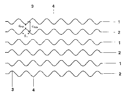
Represented in Figure 1 is a schematic illustration of
an electrode configuration of anodes 1 and cathodes 2
which alternate in individual strips and run
essentially parallel to one another. Disregarding a
right-hand and a left-hand straight connecting piece,
in this case all anodes 1 and cathodes 2 have a
sinusoidal meandering shape, immediately adjacent
anodes 1 running in phase with one another and
immediately adjacent cathodes 2 running in phase with
one another, and immediately adjacent anodes and
cathodes running, in turn, in phase opposition with cne
another.
If upwardly pointing bows 3 of the sinusoidal shape are
denoted in Figure 1 as maxima, and downwardly pointing
bows 4 are denoted as minima, cathode maxima 3
therefore meet anode minima 4 and vice versa, that is
to say they are respectively opposite one another in an
immediately adjacent fashion. Consequently, the points
of highest field strength are respectively situated
between a maximum 3 and a minimum 4.
Individual discharge structures, which are not
illustrated here, initially form at these points. Given
CA 02345684 2001-03-28
- 18 -
adequate power coupling, all preferred points are
occupied by a respective individual discharge
structure. AccordincC to the invention, a further rise
in the power feed, for example through an increase in
the amplitude of the external voltage applied to the
discharge lamp, now leads to a widening of the
respective individual discharge structures from the
region of the immediate maxima 3 and minima 4. In this
case, a corresponding power control device of a ballast
can be used to raise the power until the individual
discharge structures are reached at the boundary
regions between the maxima 3 and the minima 4, that is
to say in the surroundings of the points of inflection.
This results in a dimming region which can be traversed
entirely continuously by means of a curtain-like
widening of the individual discharge structures.
Reference is made for this purpose to the parallel
application already incorporated by reference.
Also illustrated in Figure 1 are the already described
geometrical variables of half period length SL, minimum
discharge spacing dmin and maximum discharge spacing
dmax- The half period length SL corresponds in this case
to the control region of the dimming function
mentioned, by virtue of the fact that the width of the
discharge structure can be set. The minimum discharge
spacing corresponds to the spacing between an
immediately adjacent maximum 3 and minimum 4. The
maximum discharge spacing does not, however, correspond
to the spacing between a maximum 3 and a minimum 4,
which respectively point to opposite sides. Rather, the
maximum discharge spacing dma,t corresponds to the
discharge spacing at the outer boundaries of the
control length SL. The adjoining half periods of the
sinusoidal wave do not belong to the control length SL,
and therefore also do not define a large= discharge
spacing dmax, because they serve the purpose of
discharges to the electrodes respectively adjacent on
CA 02345684 2001-03-28
- 19 -
the opposite side (for example not used for discharges
in the case of edge electrodes).
A largely identical structure is shown in Figure 2, but
in this case a cutout in the line drawn between the
maxima 3 and the minima 4 in the region 5 of the points
of inflection is intended to indicate a thickening of
the dielectric layer present there.
Specifically, in the case of all the exemplary
embodiments illustrated here the anodes 1 and the
cathodes 2 are symmetrical, that is to say cannot be
distinguished from one another. Consequently, both
types of electrode are covered with a dielectric layer.
The regions 5 in F:Lgure 2 correspond to an increased
layer thickness of the dielectric.
The already-described variants, associated with the
grain size of the fluorescent material, of a particular
structuring of these regions 5 between meanders are
also possible here.
With regard to the first variant, thus designated, of
the invention, there is virtually no divergent
representation in the figures; all that would be
required in Figure 'L is to imagine a dielectric coating
of the anodes 1 and cathodes 2 which alternates in
layer thickness, or an alternating coating and non-
coating.
An alternative meandering shape is shown in Figure 3,
specifically a shape of the type of a rectangular wave
for the anodes 1 and cathodes 2. Consequently, the
maxima 3 and the minima 4 are not localized in this
example, but correspond to a half period of the
respective electrode strip.
CA 02345684 2001-03-28
- 20 -
In this example, thi=_refore, nose-like projections 6 are
provided on the maxima 3 and minima 4, and face the
respectively adjacent minima 4 or maxima 3.
These nose-like projections 6 facilitate the initial
striking of discharge structures, and fix the discharge
structures centrally in the regions, expanded in this
example, of the maximum field between the electrode
strips as long as the power supply does not lead to a
widening of the discharge structures over the entire
width of the half period.
The abovementioned geometrical variables are also
illustrated in Figure 3. The half period length SL
corresponds to the linear extent of the maxima 3 or
minima 4. The minimum discharge spacing dmin corresponds
to the spacing between the described nose-like
projections 6, wher_eas the maximum discharge spacing
corresponds to the discharge spacing in the adjacent
straight region of the electrodes. It is clear in this
figure that the minimum discharge spacing dmin is only
slightly smaller than the maximum dmax.
A facilitated striking can, however, also be performed
by the meandering shape as such, as shown by the
example in Figure 4 with a sawtooth shape.
Here, the reference numerals 3 and 4 denote the
respective meanders of the saw tooth, that is to say
the regions around a maximum and minimum. The maxima
and minima themselves correspond respectively to a
punctiform corner 7, which therefore has the function
of facilitating striking in the same way as the nose-
like projections 6 already discussed with the aid of
Figure 3.
Once again, the geornetrical reference variabl:,s SL, dmin
and dmaxi which have been repeatedly mentioned, are
CA 02345684 2001-03-28
- 21 -
illustrated in Figure 4, the explanation here being
similar to Figure 1.
Of course, it is also possible in the case of this
exemplary embodiment to provide measures, as with the
example in Figure 2, in the case of the regions between
meanders which correspond here to the middle regiori of
each straight section of the sawtooth shape. However,
this is not illustrated separately.
Figure 5 shows electrode tracks in the shape of
semicircular waves, that is to say the shape of each
electrode corresponds to a sequence of semicircles
which are joined to one another alternately in mirror
fashion relative to the longitudinal axis of the
respective electrode track, this being done in such a
way that the upwardly pointing semicircular arcs 3 can
be denoted as maxima, and the downwardly pointing
semicircular arcs 4: as minima. In other words, the
electrode tracks in Figure 5 can be conceived as having
been produced from -those in Figure 1 by virtue of the
fact that each sinusoidal half wave has been replaced
by an appropriate in-phase semicircle.
The following dimensions (in mm) hold for the
geometrical variables of minimum discharge spacing dminr
maximum discharge spacing dma~ and half period length SL
for the exemplary embodiments in Figures 1, 2, 3, 4 and
5:
Example djõ d,,,,. SL
Figure 1 5 8 9
Figure 2 5 6 6
Figure 3 5 6 ~
Figure 4 6 10 17
Figure 5 4 8 ~
In the overall comparison of the electrode
configurations illustrated in Figures 1-5, Figure 4 is
CA 02345684 2001-03-28
- 22 -
distinguished by a particularly favourable striking
performance.
The example in Figure 3 is less favourable for various
reasons, firstly because of the relatively large
capacitance owing to the electrode strips, which run
close to one another over a relatively wide region.
Secondly, disregarding the respective nose 6, in the
region of the extended maxima 3 and minima 4 there is
here no further pro:nounced dependence of the discharge
preconditions on location, for which reason this
structure is initially poorly suited to power control.
However, it would be possible here to use other
measures than varying the discharge spacing - as in
examples in Figures 1, 2 and 4 - to create such an
inhomogeneity, for example varying the electrode width.
Only then can the half period width SL be denoted as
control length. Reference may be made once again, for
this purpose, to the already cited parallel application
regarding power control.
By contrast with the sinusoidal shape in Figures 1 and
2, the sawtooth shape in Figure 4 has, in turn, the
disadvantage that, because of the corners 7 of the
sawtooth shape, there is also a certain concentration
of current on the ariode side of a discharge structure -
in the bipolar case, the instantaneous anode side.
However, for the purpose of optimizing the overall
efficiency of the discharges and the discharge lamp,
efforts must be made to extend the individual
discharges in themselves as far as possible spatially,
and to create regions of increased charge carrier
concentration which are as few or small as possible.
The double sinusoidal shape illustrated in Figures ~
and 2 therefore offers a favourable compromise as
regards the efficiency of the discharges, the overall
capacitance, the power control properties, the
CA 02345684 2001-03-28
- 23 -
achievable surface luminance and the uniformity of this
luminance.
The semicircular waveform shape illustrated in Figure 5
is distinguished f.'rom the sinusoidal shape illustrated
in Figures 1 and 2 by shallower gradients in the region
of the control length SL, which has a positive effect
on the controllabil.ity of power, that is to say the
dimming performance. For this reason an exemplary
embodiment based on the electrode configuration
illustrated in Figui-e 5 may be explained in more detail
below. This is a flat lamp with a discharge vessel (not
illustrated) which is formed from a baseplate and a
front plate as well as a circumferential frame. The
plates consist of glass of thickness 2 mm and
dimensions of 105 mm by 137 mm. The height and width of
the frame are both 5 mm. The inner area of the
baseplate is 78 mm by 110 mm. The electrode
configuration in Fig-are 5 is arranged on the baseplate
and covered with a glass solder (not illustrated) with
a thickness of approximately 150 pm (discharge
dielectrically impeded on both sides) Consequently,
this flat lamp is also suitable for the bipolar variant
of the operating method. Moreover, a light-reflecting
layer made from A1203 or Ti02 is applied to the
baseplate and the frame. A three-band fluorescent layer
follows thereafter on all inner surfaces. The discharge
vessel is filled with xenon at a pressure of
approximately 13 kPa. In the case of a unipolar mode of
operation and a voltage pulse frequency of 80 kHz, it
is possible using the peak voltage as controlled
variable to influerice the widths of the delta-shaped
partial discharges (not illustrated) in the region of
the respective control length SL. The average power
consumption can be increased from 7 W to 10 W in this
way, given an increase in the peak voltage f_rom 1.39 kV
to 1.49 kV.
CA 02345684 2007-06-08
77332-94
- 24 -
Further details on the shape and structure of the
characteristic partial discharges produced by the
pulsed operation of dielectrically impeded discharges
under various operating conditions are to be found in
WO 94/23442, already cited.
The electrode configurations illustrated here are all
provided for flat radiators such as are described in
the earlier application WO 98/43277, for example.
As regards further technical
details, reference may also be made to the parallel
application, already repeatedly mentioned, entitled
"Dimmbare Entladungslampe fur dielektrisch behinderte
Entladungen" ["Dimmable discharge lamp for
dielectrically impeded discharges"] with the file
reference DE 198 44 720.5.
Figure 6 shows a schematic circuit diagram of a ballast
which is designed for the bipolar variant of the
operating method. Thus, external voltage pulses of
alternating polarity are applied to the dielectrically
impeded discharge lamp L, for example of the type
described in relation to Figure 5. For this purpose,
the transformer T has two primary windings which are
illustrated in Figure 6 with an opposite winding sense.
Each of the primary windings is connected electrically
in series to an assigned switching transistor TQ with a
dedicated control device SE. Of course, the two control
devices can also be understood as two functions of a
unitary control device; the aim is merely to symbolize
that the two primary windings are not clocked jointly,
but alternately. Because of the reversal in winding
sense between the two primary windings, upon clocking
of the primary windings the transformer T respectively
produces voltage pulses of opposite polarity in the
secondary ci rcui t S. To summarize, in the case of the
circuit in Figure 1 the module comprising the primary
winding W1, the switch TQ and the control device SE is
CA 02345684 2001-03-28
- 25 -
of double design, a reversal of sign being effected by
the winding sense.
Figure 7 shows corresponding real measurement curves of
the external lamp voltage UL and the lamp current IL,. It
is to be borne in rr.i.nd here that the measured external
lamp voltage UL is composed of the voltage of the
actual pulse and the voltage of the natural oscillation
of the secondary circuit. However, at least the latter
has no decisive influence on the discharge. What is
decisive, rather, are the actual voltage pulses which
effect the corresponding lamp current pulses of the
striking and the restriking and finally result in the
operation using active power pulses already disclosed
in WO 94/23442. The fact that there is a bipolar
operating method cari be detected both from the striking
pulses of the external lamp voltage and from the lamp
current pulses of the striking and the restriking.