Note: Descriptions are shown in the official language in which they were submitted.
CA 02345845 2010-06-01
-1-
BITLINE PRECHARGE
FIELD OF THE INVENTION
The present invention relates to content addressable memory (CAM). In
particular,
the present invention relates to a circuit and method for high speed
precharging of bitlines in
an open bitline architecture CAM device.
BACKGROUND OF THE INVENTION
In many conventional memory systems, such as random access memory, binary
digits
(bits) are stored in memory cells, and are accessed by a processor that
specifies a linear
address that is associated with the given cell. This system provides rapid
access to any
portion of the memory system within certain limitations. To facilitate
processor control, each
operation that accesses memory must declare, as a part of the instruction, the
address of the
memory cell/cells required. Standard memory systems are not well designed for
a content
based search. Content based searches in standard memory require software based
algorithmic
search under the control of the microprocessor. Many memory operations are
required to
perform a search. These searches are neither quick nor efficient in using
processor resources.
To overcome these inadequacies an associative memory system called Content
Addressable Memory (CAM) has been developed. CAM allows cells to be referenced
by
their contents, so it has first found use in lookup table implementations such
as cache
memory subsystems and is now rapidly finding use in networking systems. CAM's
most
valuable feature is its ability to perform a search and compare of multiple
locations as a
single operation, in which search data is compared with data stored within the
CAM.
Typically search data is loaded onto search lines and compared with stored
words in the
CAM. During a search-and-compare operation, a match or mismatch signal
associated with
each stored word is generated on a matchline, indicating whether the search
word matches a
stored word or not. A typical word of stored data includes actual data with a
number
appended header bits, such as an "E" bit or empty bit for example, although
the header bits
are not specifically searched during search-and-compare operations.
A CAM stores data in a matrix of cells, which are generally either SRAM based
cells
or DRAM based cells. Until recently, SRAM based CAM cells have been most
common
because of their simple implementation. However, to provide ternary state
CAMs, ie. where
CA 02345845 2010-06-01
-2-
the search and compare operation returns a "0", "1" or "don't care" result,
ternary state
SRAM based cells typically require many more transistors than a DRAM based
cells. As a
result, ternary state SRAM based CAMs have a much lower packing density than
ternary
DRAM cells.
A typical CAM block diagram is shown in Figure 1. The CAM 10 includes a
matrix,
or array 100, of DRAM based CAM cells (not shown) arranged in rows and
columns. An
array of DRAM based ternary CAM cells have the advantage of occupying
significantly less
silicon area than their SRAM based counterparts. A predetermined number of CAM
cells in
a row store a word of data. An address decoder 17 is used to select any row
within the CAM
array 100 to allow data to be written into or read out of the selected row.
Data access circuitry
such as bitlines and column selection devices, are located within the array
100 to transfer data
into and out of the array 100. Located within CAM array 100 for each row of
CAM cells are
matchline sense circuits, which are not shown, and are used during search-and-
compare
operations for outputting a result indicating a successful or unsuccessful
match of a search
word against the stored word in the row. The results for all rows are
processed by the priority
encoder 22 to output the address (Match Address) corresponding to the location
of a matched
word. The match address is stored in match address registers 18 before being
output by the
match address output block 19. Data is written into array 100 through the data
UO block 11
and the various data registers 15. Data is read out from the array 100 through
the data output
register 23 and the data 1/0 block 11. Other components of the CAM include the
control
circuit block 12, the flag logic block 13, the voltage supply generation block
14, various
control and address registers 16, refresh counter 20 and JTAG block 21.
Figure 2 shows a typical ternary DRAM type CAM cell 140 as described in
Canadian
Patent No. 2,266,062, issued March 30, 2004. Cell 140 has a comparison circuit
which
includes an n-channel search transistor 141 connected in series with an n-
channel compare
transistor 142 between a matchline ML and a tail line TL. A search line SL* is
connected to
the gate of search transistor 141. The storage circuit includes an n-channel
access transistor
143 having a gate connected to a wordline WL and connected in series with
capacitor 144
between bitline BL and a cell plate voltage potential VCP. Charge storage node
CELL1 is
connected to the gate of compare transistor 142 to turn on transistor 142 if
there is charge
stored on capacitor 144 i.e. if CELL1 is logic "1". The remaining transistors
and capacitor
replicate transistors 141, 142, 143 and capacitor 144 for the other half of
the ternary data bit,
CA 02345845 2010-06-01
-3-
and are connected to corresponding lines SL and BL* and are provided to
support ternary
data storage. Together they can store a ternary value representing logic "I",
logic "0", or
"don't care".
Ternary Value CELL1 CELL2
0 0 1
1 1 0
"Don't Care" 0 0
The tail line TL is typically connected to ground and all the transistors are
n-channel
transistors. The description of the operation of the ternary DRAM cell is
detailed in the
aforementioned reference.
As previously mentioned, memory array 100 uses DRAM type memory cells to
attain
a higher density of cells per unit area of silicon, which has the benefit of
reducing the overall
cost of manufacturing. However, within the field of DRAM memory, there are two
well
known architectures used for arranging the memory cells and bitlines, which
when applied to
the ternary CAM of the present invention, each provide distinct advantages and
disadvantages to the CAM device.
The first architecture is the open bitline architecture, generally shown in
Figure 3.
The arrangement shown in Figure 3 is representative of the physical layout of
the bitlines
with respect to the bitline sense amplifier (BLSA) on a fabricated device.
Wordlines,
memory cells and read/write circuits are intentionally omitted to simplify the
schematic. But
it will be understood by those skilled in the art that wordlines would run
perpendicular to the
bitlines, memory cells would be located near the intersection between each
wordline and
bitline, and read/write circuits are coupled to the bitlines. Complementary
bitlines 32 and 34
extend away from the left and right sides of the bitline sense amplifier
(BLSA) 33. A bitline
sense amplifier such as BLSA 33 is well known in the art and typically
includes a pair of
cross-coupled complementary pair of CMOS transistors. An n-channel
equalization transistor
31 is connected between bitlines 32 and 34 for electrically shorting the two
bitlines together,
and has a gate controlled by a bitline equalization signal BLEQ. Bitlines 32
and 34,
equalization transistor 31 and BLSA 33 form one open bitline pair. Another
bitline pair
CA 02345845 2010-06-01
-4-
consisting of bitlines 36 and 37, equalization transistor 35 and BLSA 38 are
configured
identically to their corresponding elements from the first open bitline pair.
In a memory
array, a plurality of open bitline pairs are arranged one below the other as
shown in Figure 3,
in which all the bitlines connected to the left side of the BLSA's are part of
the left sub-array
and all the bitlines connected to the right side of the BLSA's are part of the
right sub-array.
For DRAM memories, it is necessary to precharge bitlines, through bitline
precharge
transistors (not shown), to a mid-point potential level prior to reading data
from a DRAM
memory cell connected to it. This mid-point potential level is typically half
the high power
supply potential used by the bitline sense amplifiers. This is to allow the
bitline sense
amplifier to detect small changes in the potential level of the bitline when
charge is added or
removed by the memory cell storage capacitor.
A brief discussion of a read and precharge operation for the open bitline
architecture
of Figure 3 follows. It is assumed that all bitlines have been precharged to a
mid-point
potential level between a high and a low logic potential level in a previous
operation. During
a read operation, one wordline of either the left or right sub-array is driven
to access one
memory cell connected to each bitline of the respective sub-array. The
bitlines of the
unaccessed sub-array remain at the mid-point potential level, which is the
reference potential
level used by the BLSA during sensing of the data on the bitlines of the
accessed sub-array.
The BLSA detects the shift in the potential level of the bitline when the
storage capacitor of
the accessed memory cell is coupled to the bitline, and amplifies and latches
the full CMOS
logic potential level of the bitline. Since BLSA is a cross-coupled latch
circuit, the accessed
bitline and its corresponding complementary bitline are driven to opposite
logic potential
levels after the data has been read out, and since the selected wordline
remains activated, the
full CMOS level is restored into the accessed cell.
To precharge the bitlines in preparation for the next read operation, control
signal
BLEQ is driven to the high logic level to turn on all equalization transistors
and short each
complementary pair of bitlines together. The bitlines having the high logic
potential level will
equalize with the bitlines having the low logic potential level through charge
sharing, such
that both reach a mid-point potential level.
The open bitline architecture allows for efficient packing of ternary CAM
memory
cells to reduce the overall area occupied by the memory array. One
disadvantage of the open
bitline architecture is unbalanced bitlines due to capacitive coupling of an
active wordline to
CA 02345845 2010-06-01
-5-
only one bitline of the complementary pair of bitlines. The bitline acting as
a reference
bitline is not crossed by an active wordline, thus it is not disturbed in the
same way as the
bitline crossing an active wordline. Therefore potential read errors may
result. Another more
significant disadvantage is the slow precharge speed. As memory densities
grow, the bitlines
become longer, which inherently have more resistance and capacitance than
shorter bitlines.
The precharge and equalization speed of the bitlines could be improved if an
additional
equalization transistor was connected between the two farthest ends of the
complementary
bitlines, instead of just at the two closest ends as shown in Figure 3.
However, it is
impractical to add such an additional equalization transistor. The metal lines
for connecting
such an additional equalization transistor would be as long as the bitlines,
hence contributing
more capacitance to the system. Therefore, when equalization is slow, the
overall access
speed of the CAM becomes slow, which restricts the CAM from being used in high
speed
applications.
The second architecture is the folded bitline architecture, generally shown in
Figure 4.
The arrangement shown in Figure 4 is representative of the physical layout of
the bitlines
with respect to the bitline sense amplifier (BLSA) on a fabricated device.
Wordlines,
memory cells and read/write circuits are intentionally omitted to simplify the
schematic. But
it will be understood by those skilled in the art that wordlines would run
perpendicular to the
bitlines, memory cells would be located near the intersection between each
wordline and
bitline, and read/write circuits are coupled to the bitlines. Complementary
bitlines 46 and 47
extend away from the left side of a shared bitline sense amplifier (BLSA) 41,
and
complementary bitlines 48 and 49 extend away from the right side of BLSA 41. A
shared
bitline sense amplifier such as BLSA 41 is well known in the art, and would
typically consist
of a pair of cross-coupled complementary pair of CMOS transistors. N-channel
equalization
transistors 42 and 43 are connected between bitlines 46 and 47 at opposite
ends of bitlines 46
and 47. Similarly, n-channel equalization transistors 44 and 45 are connected
between
bitlines 48 and 49 at opposite ends of bitlines 48 and 49. Equalization
transistors 42 and 43
have gates controlled by a left sub-array bitline equalization signal BLEQ_L,
and
equalization transistors 44 and 45 have gates controlled by a right sub-array
bitline
equalization signal BLEQ_R. In a typical array, a shared BLSA and respective
pairs of
folded bitlines are arranged in a column, and several columns can be arranged
side by side.
In Figure 4, bitlines 46 and 47 and equalization transistors 42 and 43 are
located within a left
CA 02345845 2010-06-01
-6-
sub-array, and bitlines 48 and 49 and equalization transistors 44 and 45 are
located within a
right sub-array.
A brief discussion of a read and precharge operation for the folded bitline
architecture
of Figure 4 follows. It is assumed that all bitlines have been precharged to a
mid-point
potential level between a high and a low logic potential level in a previous
operation. During
a read operation, one wordline of either the left or right sub-array is driven
to access one
memory cell connected each bitline, BLO or BLO* for example, of the respective
sub-array,
and the corresponding equalization control signal, BLEQ_L or BLEQ_R is turned
off. The
folded complementary bitlines of the unaccessed sub-array, BLI and BL1 * for
example,
remain at the precharged mid-point potential level. If a memory cell connected
to BLO is
accessed by the driven wordline, then the complementary bitline BLO* remains
at the
precharged mid-point potential level, which is the reference potential level
used by BLSA 41.
Accordingly, the role of each bitline is reversed if a memory cell connected
to BLO* is
accessed instead of a memory cell connected to BLO. Furthermore, the roles of
both folded
bitline pairs is reversed if a driven wordline accesses a memory cell
connected to either BL1
or BL1*. Since BLSA is a cross-coupled latch circuit, the accessed bitline and
its
corresponding complementary bitline are driven to opposite logic potential
levels after the
data has been read out. To precharge the bitlines in preparation for the next
read operation,
the equalization signal (BLEQ_L or BLEQ_R) for the accessed sub-array is
driven to the
high logic level to turn on its respective equalization transistors. The
bitlines having the high
logic potential level will equalize with the bitlines having the low logic
potential level
through charge sharing, such that both reach a mid-point potential level. The
bitlines of the
unaccessed sub-array remain precharged throughout the read operation. Because
equalization
transistors 42, 43 and 44, 45 are placed near the two extremities of their
respective folded
bitline pairs, the time required for equalization is short when compared to
the equalization
speed of the open bitline architecture shown in Figure 3.
Given that the bitlines of Figures 3 and 4 are the same length and width, the
time
constant for each bitline in Figure 3 is expressed as -open = RC, where R is
the lumped
resistance and C is the lumped capacitance of the bitline. Each bitline of
Figure 4 has half the
resistance and capacitance of a bitline of Figure 3 due to the additional
equalization transistor
placed at the extremities of the folded bitlines. Therefore, relative to the
bitlines of Figure 3,
CA 02345845 2010-06-01
-7-
R C
the time constant is expressed as zfolded = i . Accordingly, the time required
for
equalizing a bitline of Figure 4 is approximately four times faster than the
time required for
equalizing a bitline of Figure 3.
There exist precharge schemes in which equalization transistors are not used
for
precharging bitlines to a mid-point potential level. Instead, a precharge
voltage is supplied
directly to the bitlines. Unfortunately, the circuit for generating such a
precharge voltage
must be of high quality, which is difficult to design and is subject to
variations in the
semiconductor fabrication process.
Despite the precharge speed advantage of the folded bitline architecture over
the open
bitline architecture, the folded bitline architecture does not allow efficient
packing of ternary
dynamic CAM cells. For highest packing density, ternary dynamic CAM cells are
arrayed as
a single line of cells under a common wordline node as well as a common
matchline node.
As such, adjacent bitlines are necessarily active during row access
operations. This excludes
the use of a folded bitline architecture which requires adjacent bitlines to
act as precharge-
level references. However, a ternary dynamic CAM memory array employing an
open bitline
architecture is not suitable for high speed applications due to its slower
precharge speed.
It is therefore desirable to provide a ternary dynamic CAM memory array
architecture
which operates at high speed and arranged with an efficient packing density to
occupy small
silicon area.
SUMMARY OF THE INVENTION
It is an object of the present invention to obviate or mitigate at least one
disadvantage
of previous ternary dynamic CAM memory array architectures. In particular, it
is an object of
the present invention to provide a ternary dynamic CAM memory array
architecture that
operates at high speed and occupies a small silicon area.
In a first aspect, the present invention provides a bitline precharge circuit
for
equalizing a first and second bitline. The circuit includes a bitline
overwrite circuit for
writing preset complementary logic potential levels onto the first and second
bitlines, and
an equalization circuit for shorting together the first and second bitlines
after the preset
complementary logic potential levels are written onto the first and second
bitlines.
In further embodiments of the present aspect, the bitline overwrite circuit
includes
CA 02345845 2010-06-01
-8-
bitline write drivers connected to respective databuses, or a local bitline
write circuit. In
another aspect of the present alternate embodiment, the local bitline write
circuit includes a
transistor for coupling the first bitline to a low logic potential level and a
transistor for
coupling the second bitline to a high logic potential level.
In yet another alternate embodiment of the present aspect, the equalization
circuit
includes at least one equalization transistor connected between the first and
second bitlines,
or two equalization transistors connected between the first and second
bitlines, where the first
and second equalization transistors are connected at opposite ends of the
first and second
bitlines, respectively.
In another aspect, the present invention provides a bitline architecture for a
ternary
content addressable memory. The bitline architecture includes a first bitline
sense amplifier
connected to first and second complementary bitlines arranged in an open
bitline
configuration, a second bitline sense amplifier connected to third and fourth
complementary
bitlines arranged in an open bitline configuration, ternary content
addressable memory cells
for storing two bits of data connected to the first and third bitlines,
ternary content
addressable memory cells for storing two bits of data connected to the second
and fourth
bitlines, a first bitline overwrite circuit for writing preset complementary
logic potential
levels onto the first and third bitlines, a second bitline overwrite circuit
for writing preset
complementary logic potential levels onto the second and fourth bitlines, a
first precharge
circuit for equalizing the first and third bitlines, and a second precharge
circuit for equalizing
the second and fourth bitlines.
In an alternate embodiment of the present aspect, the first and second bitline
sense
amplifiers include CMOS cross coupled inverters. In another alternate
embodiment of the
present aspect, the ternary content addressable memory cells are ternary DRAM
type CAM
cells.
In a further aspect of the present invention, there is provided a content
addressable
memory. The content addressable memory consists of content addressable memory
cells
arranged in rows and columns, each cell having a first and second bitline, a
bitline overwrite
circuit for each pair of first and second bitlines for writing preset
complementary logic
potential levels onto the first and second bitlines, an equalization circuit
for each pair of first
and second bitlines for shorting together the first and second bitlines after
the preset
CA 02345845 2010-06-01
-9-
complementary logic potential levels are written onto the first and second
bitlines, an address
decoder for addressing rows of cells, write data circuitry for writing data to
the cells, and
read circuitry for reading data from the cells.
In yet another aspect of the present invention, there is provided a method for
precharging first and second bitlines in a content addressable memory. The
method consists
of writing preset complementary logic potential levels onto the first and
second bitlines, and
equalizing the first and second complementary signal lines.
BRIEF DESCRIPTION OF THE DRAWINGS
Embodiments of the present invention will now be described, by way of examples
only, with reference to the attached Figures, wherein
Figure 1 shows a block diagram of a CAM according to an embodiment of the
present
invention;
Figure 2 shows a schematic of a DRAM based CAM cell;
Figure 3 illustrates an open bitline architecture of the prior art;
Figure 4 illustrates a folded bitline architecture of the prior art;
Figure 5 illustrates a generic bitline precharge and equalize architecture
according to
the invention;
Figures 6A and 6B show a detailed circuit schematic of the bitline precharge
and
equalize architecture of Figure 5; and,
Figure 7 shows a schematic of a local bitline overwrite circuit.
DETAILED DESCRIPTION
Generally, the present invention provides a bitline architecture and method
for fast
equalization of bitlines in a densely packed, ternary dynamic content
addressable memory.
More specifically, the bitline architecture of the present invention is a
hybrid architecture
combining the high density of open bitline architectures and the fast
precharge speed of
folded bitline architectures. Data read and write operations are performed in
a manner
consistent with traditional open bitline architectures, but bitline precharge
and equalization is
performed in a manner consistent with traditional folded bitline
architectures.
Figure 5 shows a general circuit diagram of the hybrid architecture of the
present
invention. Various control signals, wordlines and read circuits are omitted to
simplify the
CA 02345845 2010-06-01
-10-
schematic. A more detailed circuit diagram showing the omitted elements of the
hybrid
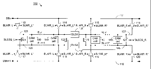
architecture is shown in Figures 6A and 6B. One row 110 of ternary CAM cells
and
associated equalization circuits is shown in Figure 5, where an array can
contain a plurality of
rows 110 arranged in column, and a plurality of columns arranged side by side.
In the
present embodiment of Figure 5, row 110 includes a pair of databuses DBn and
DBn+l
denoted by reference numerals 111 and 112 respectively, tri-state inverters
113, 114, 115,
116, 117, 118, 119 and 120, two pairs of first and second bitlines BLn, BLn*
and BLn+l,
BLn+l * denoted by reference numerals 125, 127 and 126, 128 respectively,
equalization
transistors 121, 122, 123 and 124, ternary CAM cells 140 and bitline sense
amplifiers 130
and 131. Bitlines 125 and 127 are configured in the open bitline architecture
with respect to
their BLSA 130, and bitlines 126 and 128 are configured in the open bitline
architecture with
respect to their BLSA 131. Each pair of first and second bitlines, BLn, BLn*
and BLn+l,
BLn+l *, do not necessarily carry only complementary data during read
operations.
However, BLn and BLn+1 are a complementary pair of bitlines as are BLn* and
BLn+l*.
Subscipt n can be any integer number greater than 0. The tri-state inverters
function as
bitline write drivers, where tri-state inverters 113, 114, 117 and 118,
bitlines 125 and 126 and
equalization transistors 121 and 122 are part of the left sub-array of row
110, and tri-state
inverters 115, 116, 119 and 120, bitlines 127 and 128 and equalization
transistors 123 and
124 are part of the right sub-array of row 110.
Because each ternary CAM cell 140 stores two bits of information, two bitlines
are
required for transferring data into and out of the cell, as previously shown
in the CAM cell
schematic of Figure 2. Therefore, when data is read out from an accessed cell,
one bit of data
is asserted onto a first bitline, BLn or BLn+l, and another bit of data is
asserted onto a
second bitline, BLn* or BLn+l*. Each complementary bitline pair is connected
to its own
bitline sense amplifier for amplifying and reading its potential level. In row
110, BLn and
BLn+1 are the first and second bitlines respectively for the ternary CAM cells
of the left sub-
array, and correspondingly, BLn+1 and BLn+l * are the first and second
bitlines respectively
for the ternary CAM cells of the right sub-array.
Equalization transistors 121 and 122 have gates connected to the left bitline
equalization signal BLSEQ_L, and have source/drain terminals connected between
BLn and
BLn+l. Equalization transistors 121 and 122 are positioned at opposite ends of
bitlines BLn
and BLn+1 with ternary CAM cells 140 positioned between them. Tri-state
inverters 113
CA 02345845 2010-06-01
-11-
and 114 drive data from databus 111 onto bitline 125, and tri-state inverters
117 and 118
drive data from databus 112 onto bitline 126. Tri-state inverters 113, 114,
117 and 118 are
enabled by complementary signals BLWR L and BLWR L*. The configuration of the
elements previously mentioned for the left sub-array of row 110 are mirrored
by their
corresponding elements for the right sub-array of row 110. Equalization
transistors 123 and
124 have gates connected to right bitline equalization signal BLEQ_R, and have
their
source/drain terminals connected between BLn* and BLn+1*. Equalization
transistors 123
and 124 are also positioned at opposite ends of bitlines BLn* and BLn+1* with
ternary CAM
cells 140 positioned between them. Tri-state inverters 115 and 116 drive data
from databus
111 onto bitline 127, and tri-state inverters 119 and 120 drive data from
databus 112 onto
bitline 128. Tri-state inverters 115, 116, 119 and 120 are enabled by
complementary signals
BLWR R and BLWR R*.
Because each complementary pair of bitlines is configured in the open bitline
architecture with respect to its bitline sense amplifier, a read operation
from the hybrid bitline
architecture of Figure 5 is executed similarly to the read operation described
for the open
bitline architecture of Figure 3. Therefore, a description of the general read
operation for the
hybrid bitline architecture of Figure 5 is not necessary. A detailed
description of the read
operation follows in the description for the detailed hybrid bitline
architecture of Figures 6A
and 6B.
The precharge and equalize operation for the hybrid bitline architecture of
Figure 5 is
described below. After a read operation, the bitline sense amplifiers 130 and
131 drive their
respective bitlines to complementary logic potential levels, hence all four
bitlines of row 110
are held at either the high or low logic potential levels. Table 1 below
illustrates the four
possible logic potential levels of the bitlines of row 110 after a read
operation is completed.
Table 1
Case BLn BLn+1 BLn* BLn+1 *
logic level logic level logic level logic level
1 1 0 1 0
2 0 1 1 0
3 1 0 0 1
4 0 1 0 1
CA 02345845 2010-06-01
-12-
To precharge the bitlines to a mid-point potential level by equalization in a
folded manner, all
first and second bitlines must have complementary logic potential levels. More
specifically,
BLn and BLn+1 of the left sub-array can have complementary logic potential
levels, and the
bitline BLn* and BLn+l* of the right sub-array can have complementary logic
potential
levels prior to turning on the equalization transistors. From Table 1 above,
the bitlines in
cases 2 and 3 can be equalized. In other words, if equalization transistors
121, 122, 123 and
124 are turned on by their respective control signals BLSEQ_L and BLSEQ_R when
the
bitlines have the logic potential levels shown in cases 2 and 3, charge
sharing will occur and
all the bitlines will equalize to a mid-point potential level between the high
and low logic
potential levels. Therefore, the precharge time of the hybrid bitline
architecture is equivalent
to the precharge time of traditional DRAM folded bitline architectures.
However, the bitlines
in cases 1 and 4 cannot be equalized because the first and second bitlines of
the left and right
sub-arrays have similar logic potential levels.
To allow equalization of the bitlines under all four cases according to the
present
invention, the first and second bitlines of both sub-arrays are overturned, or
overwritten with
preset complementary logic potential levels from the databuses DBn and DBn+l
prior to
equalization. For example, a high logic potential level can be written onto
databus DBn and a
low logic potential level can be written onto databus DBn+l after the read
operation.
Therefore, BLn and BLn* are driven to the low logic potential level via tri-
state inverters
113, 114, 115 and 116, and BLn+1 and BLn+l* are driven to the high logic
potential level
via tri-state inverters 117, 118, 119 and 120. Now that all first and second
bitlines have
complementary logic potential levels, equalization transistors 121, 122, 123
and 124 are
turned on and all bitlines of the left and right sub-arrays equalize to a mid-
point potential
level. Alternatively, the logic potential levels written onto databuses DBn
and DBn+1 can be
reversed to drive complementary logic level potential levels onto the first
and second bitlines.
Although not shown, overwrite circuitry including global write drivers can be
configured to
write the preset data onto the databuses, or additional drivers can be
directly connected to the
databuses. However, there are several methods for writing preset data to the
databuses,
which should be apparent to those skilled in the art.
A detailed circuit diagram of the hybrid bitline architecture according to an
embodiment of the present invention is shown in Figures 6A and 6B. Wordlines
and memory
cells are not shown to simplify the schematic. But it will be understood by
those skilled in the
CA 02345845 2010-06-01
-13-
art that the wordlines would run perpendicular to the bitlines and the memory
cells would be
located at the intersection of each wordline and bitline. Many elements shown
in Figure 5
correspond with elements of Figures 6A and 6B having the same reference
numerals. Figures
6A and 6B illustrate the read, write and precharge circuits associated with
one row of ternary
CAM cells. A plurality of such rows can be arranged in a column, and a
plurality of columns
can be arranged side by side in a CAM memory array. In the present embodiment,
the first
and second bitlines of the left and right sub-arrays of the row are each
connected to 128
ternary CAM cells. It is noted that the number of cells connected to each pair
of first and
second bitlines depends on the desired size of the memory array, thus
alternate embodiments
could have more or less than 128 ternary CAM cells per pair of first and
second bitlines. The
hybrid bitline architecture of Figures 6A and 6B includes bitline read
circuitry, bitline write
circuitry and bitline precharge circuitry. The internal nodes labelled a, b, c
and d in Figure
6A are connected to the same labelled nodes in Figure 6B.
The bitline read circuitry for BLn and BLn+1 includes bitline sense amplifier
130,
transfer gates 157 and 158 and databus read drivers 149, 150 and 151, 152.
Bitline sense
amplifier 130 includes a pair of cross-coupled inverters. A first inverter
includes p-channel
transistor 153 and n-channel transistor 154 serially connected between restore
voltage PR and
sense voltage PSb. A second inverter includes p-channel transistor 155 and n-
channel
transistor 156 serially connected between restore voltage PR and sense voltage
PSb. PR and
PSb are controlled internal high and low power supply voltages, respectively,
for all the
bitline sense amplifiers 130. The output of the first inverter is connected to
a first terminal of
n-channel transfer gate 157 and the output of the second inverter is connected
to a first
terminal of n-channel transfer gate 158. Transfer gates 157 and 158 are
controlled by signal
TG, for connecting the bitline sense amplifier 130 to bitlines BLn and BLn* at
their
respective second terminals during a read operation. A first databus read
driver includes re-
channel transistors 149 and 150 serially connected between DBn and VSS. The
gate of
transistor 149 is connected to a read left sub-array signal RD_L, and the gate
of transistor
150 is connected to the output of the first inverter of bitline sense
amplifier 130. A second
databus read driver includes n-channel transistors 151 and 152 serially
connected between
DBn and VSS. The gate of transistor 151 is connected to a read right sub-array
signal
RD_R, and the gate of transistor 152 is connected to the output of the second
inverter of
bitline sense amplifier 130. Bitline read circuitry for BLn+1 and BLn+l * are
configured
CA 02345845 2010-06-01
-14-
identically to the bitline read circuitry for BLn and BLn* previously
described. Transistors
163, 164, 165 and 166 of the bitline sense amplifier 130 correspond with
transistors 153, 154,
155 and 156 respectively. Transfer gates 167 and 168 correspond with
transistors 157 and
158 respectively. Databus read driver transistors 159, 160 and 161, 162
correspond with
transistors 149, 150 and 151, 152 respectively.
The bitline write circuitry includes tri-state inverters 113, 114, 115, 116,
117, 118,
119 and 120. Generally, two tri-state inverters drive databus data onto each
bitline, where
each tri-state inverter has p-channel transistors 131 and 132 serially
connected between the
voltage supply VDD and a bitline, and n-channel transistors 133 and 134
serially connected
between the bitline and the voltage supply VSS, or ground. Enabling
transistors 131 and 134
of each tri-state inverter have gates connected to a bitline write signal and
a complementary
bitline write signal. A complementary pair formed by transistors 132 and 133
of each tri-
state inverter have gates connected to its respective databus. A more detailed
description of
the tri-state inverters follows. Tri-state inverter 113 is connected to
bitline BLn at
approximately the farthest position from the bitline sense amplifier 130, and
tri-state inverter
114 is connected to bitline BLn at approximately the closest position from the
bitline sense
amplifier 130. Both tri-state inverters 113 and 114 have enabling transistors
131 and 134
connected to left sub-array write signal BLWR L* and its complement BLWR L
respectively, and have their complementary pair of transistors 132 and 133
connected to
databus DBn. Tri-state inverters 117 and 118 are connected to bitline BLn+1 at
the same
positions as tri-state inverters 113 and 114 connected to bitline BLn. Both
tri-state inverters
117 and 118 also have enabling transistors 131 and 134 connected to left sub-
array write
signal BLWR L* and its complement BLWR L respectively, but have their
complementary
pair of transistors 132 and 133 connected to databus DBn+1. Tri-state
inverters 115, 116 and
119, 120 are similarly connected to their respective bitlines BLn* and BLn+1
*. The
enabling transistors 131 and 134 of tri-state inverters 115, 116, 119 and 120
are connected to
right sub-array write signal BLWR R* and its complement BLWR R respectively.
The
complementary pair of 132 and 133 of tri-state inverters 115, 116 and 119, 120
are connected
to databuses DBn and DBn+1 respectively.
The bitline precharge circuitry includes n-channel equalization transistors
121, 122,
123, 124, 169 and 170, and n-channel bitline precharge transistors 147, 148,
172 and 174.
Although the tri-state inverters are part of the write circuitry, they are
also a part of the bitline
CA 02345845 2010-06-01
-15-
precharge circuitry in the present embodiment during precharge operations. A
description of
the precharge circuits for the left sub-array of the row now follows.
Equalization transistor
121 has its source/drain terminals connected to BLn and BLn+1 at approximately
the farthest
position from the bitline sense amplifier 130. Equalization transistor 122
also has its
source/drain terminals connected to BLn and BLn+1, but at approximately the
closest
position from the bitline sense amplifier 130. Thus, equalization transistors
are connected at
opposite ends of the pair of first and second bitlines. Precharge transistor
147 couples bitline
precharge voltage VBLP to BLn and precharge transistor 148 couples bitline
precharge
voltage VBLP to BLn+1. The precharge transistors can be connected to their
respective
bitlines at any convenient location along the bitlines. Equalization
transistors 123 and 124,
and bitline precharge transistors 172 and 174 of the right sub-array are
connected to bitlines
to BLn* and BLn+1* in the same configuration as described for their
corresponding
transistors of the left sub-array. Additional equalization transistors 169 and
170 have their
source/drain terminals connected to the outputs of their respective bitline
sense amplifier
cross-coupled inverters. All the equalization transistors and precharge
transistors have their
gates connected to a bitline equalization signal BLSEQ.
The following description of the read, write and precharge operations are made
with
reference to Figures 5, 6A and 6B, and more specifically, the circuits
connected to bitlines
BLn and BLn+1.
The read operation for the hybrid bitline architecture of the present
invention is
similar to the read operation for the open bitline architecture described in
Figure 3. It is
assumed that bitlines BLn and BLn+1 have been precharged to the mid-point
potential level,
and databus DBn has been precharged to the high potential level after a
previous operation.
Signals RD_L and RD_R are inactive at the low logic potential level, and
signal TG is at the
high logic potential level to connect the bitline sense amplifiers to their
respective bitlines.
Signals PR and PSb are held at a midpoint potential level of the bitlines. To
read data from
the bitlines, one wordline from either the left or right sub-array is
activated to access one of
128 ternary CAM cells connected to each pair of first and second bitlines. If
the ternary
CAM cell of Figure 2 is used in the array, the active wordline would be driven
to VPP, a
potential level higher than VDD. Depending on the stored data in the accessed
CAM cell,
charge is either added to its corresponding bitline to increase its potential
level above the
mid-point potential level, or removed from its corresponding first bitline to
decrease its
CA 02345845 2010-06-01
-16-
potential level below the mid-point potential level. It is noted that the
bitline of the
unaccessed sub-array remains at the precharged mid-point potential level since
no wordline in
that sub-array is activated, and hence serves as a reference bitline for
bitline sense amplifier
130. Bitline sense amplifier voltages PR and PSb are driven to their
respective internal high
and low potential levels to activate the bitline sense amplifier. Bitline
sense amplifier 130
then compares the accessed bitline to the reference potential level of the
reference bitline. If
the accessed bitline has a potential level less than the reference potential
level, then the logic
"0", or low potential level is latched. Alternatively, if the accessed bitline
has a potential
level greater than the reference potential level, then the logic "I", or high
potential level is
latched. Accordingly, once bitline sense amplifier 130 latches the data of the
accessed bitline,
the reference bitline is driven to the opposite logic level. A bitline driven
to the high
potential level by bitline sense amplifier 130 turns on its respective read
transistor, 150 or
152. Signal TG is driven to the low logic potential level shortly after
signals PR and PSb are
driven to their respective high and low potential levels. Once the transfer
gate transistors are
turned off, BLSA latching is completed without being loaded by the bitline
capacitance.
Depending on the sub-array being accessed, either read left sub-array signal
RD_L or either
read right sub-array signal RD_R is driven to the high potential level to turn
on read enable
transistors 149 or 151 respectively. If a pair of serially connected read
enable and read
transistors, 149 and 150 for example, are turned on, then DBn is discharged to
ground.
Otherwise, DBn remains at the precharged high potential level. Tri-state
inverters 113, 114,
115 and 116 are turned off during the bitline read access operation by driving
signals
BLWR L*, BLWR R* to the high potential level and signals BLWR L, BLWR R to the
low potential level. However, the tri-state inverters can be turned on at the
end of the read
operation to restore the bitline potential to the VDD supply rail. This
particular feature of the
circuit is described in further detail later. Although the previous
description of the read
operation has been made with reference to the circuits connected to bitlines
BLn and BLn+1,
the same description also applies to the circuits connected to bitlines BLn*
and BLn+1*.
Writing data to the bitlines does not involve the previously described read
circuitry,
but still requires activation of one wordline from either the left or right
sub-array in order to
access one of 128 ternary CAM cells connected to each pair of first and second
bitlines.
Transfer gates 157 and 158 and read enable transistors 149 and 151 are turned
off during the
write operation to isolate the bitline sense amplifier 130 from bitlines BLn
and BLn+1 and
CA 02345845 2010-06-01
-17-
databus DBn. It is assumed that bitlines BLn and BLn+1 have been precharged to
the mid-
point potential level, databus DBn has been driven with high or low potential
level write data
from global write drivers (not shown), and sub-array bitline write signals
BLWR L*,
BLWR R* and BLWR L, BLWR R are at the high and low potential levels
respectively
to keep tri-state inverters 113, 114, 115 and 116 initially turned off.
Depending on the
potential level of DBn, one of transistors 132 and 133 of tri-state inverters
113 and 114 is
turned on. A pair of complementary sub-array write signals associated with the
active
wordline, BLWR L*, BLWR L or BLWR R*, BLWR_R are subsequently driven to the
low and high potential levels respectively. Therefore only tri-state inverters
113, 114 or 115,
116 are turned on to drive write data from DBn onto bitlines BLn or BLn+1
respectively.
Depending on the potential level of DBn, a high or low potential level is
driven onto the
bitlines. Although the previous description of the write operation has been
made with
reference to the circuits connected to bitlines BLn and BLn+l, the same
description also
applies to the circuits connected to bitlines BLn* and BLn+1*.
Following a read or write operation, the bitines are precharged to the mid-
point
potential level in preparation for a subsequent read operation. Transfer gates
157 and 158 are
initially turned off and read enable transistors 149 and 151 remain turned off
during the
precharge operation to isolate the bitline sense amplifier 130 from bitlines
BLn and BLn+1
and databus DBn. Bitline sense amplifier voltages PR and PSb are driven to the
mid-point
potential level to disable the bitline sense amplifiers. Databuses DBn and
DBn+1 are first
driven by the global write drivers with preset complementary logic potential
levels, followed
by activation of the left and right sub-array tri-state inverters and transfer
gates 157, 158, 167
and 168. In other words, signals BLWR L*, BLWR_R* and BLWR L, BLWR R are
driven to the low and high potential levels respectively, and signal TG is
driven to the high
potential level. Therefore, previous logic potential levels on the bitlines
from the previous
read/write operation are overwritten, or overturned with the preset logic
potential levels. For
example, if DBn and DBn+1 are driven to the high and low potential levels
respectively, then
bitlines BLn, BLn* are driven to the low potential level via tri-state
inverters 113, 114, 115
and 116, and bitlines BLn+l, BLn+1* are driven to the high potential level via
tri-state
inverters 117, 118, 119 and 120. The tri-state inverters remain active until
all bitlines are fully
driven to their final complementary levels. Then signals BLWR L*, BLWR R* and
BLWR L, BLWR_R are driven to the high and low potential levels respectively to
disable
CA 02345845 2010-06-01
-18-
the tri-state inverters. At this point, bitline equalization can occur.
Bitline equalization signal
BLSEQ and transfer gate signal TG are then driven to the high potential level
to turn on the
precharge circuitry and the transfer gates. Specifically, equalization
transistors 121, 122,
123, 124, 169 and 170 are turned on to short all four bitlines together, and
transfer gates 157,
158, 167 and 168 are turned on so that the complementary bitline pairs are
coupled together
via equalization transistors 169 and 170. All four bitlines eventually
equalize to the mid-
point potential level through charge sharing. Precharge transistors 147, 148
172 and 174 are
also turned on to couple bitline precharge voltage VBLP to all the bitlines,
to hold the
bitlines at the mid-point VBLP potential level. VBLP is a mid-point potential
level produced
from a voltage generator which is not shown.
The hybrid bitline architecture of the present invention has several
advantages over
the bitline architectures of the prior art. The precharge operation is
executed in a manner
consistent with folded bitline architectures, and hence about four times
faster than for
traditional open bitline architectures having the same length bitlines because
of the additional
equalization transistors connected at the opposite ends of each pair of first
and second
bitlines. Since the bitlines are initially precharged to the mid-point
potential level via
equalization, a VBLP generator designed with less restrictions can be used to
maintain the
mid-point potential levels on the bitlines. The open bitline architecture
allows for maximum
packing efficiency of ternary dynamic CAM cells within an array to keep area
consumption
and consequently costs, low.
Although databuses DBn and DBn+1 are shown as being in parallel with the
bitlines,
alternate embodiments can have DBn and DBn+1 formed as segments connected to
global
databuses formed perpendicularly to the segments.
In another alternate embodiment of the present invention shown in Figure 7,
additional local overwrite circuits are connected to the bitlines for driving
the bitlines to the
predetermined data potential levels instead of using the write drivers and
databuses for
writing the predetermined data to the bitlines. Bitlines BLn and BLn+I are
shown in Figure
7, where p-channel overwrite transistor 180 couples VDD to BLn and n-channel
overwrite
transistor 182 couples ground to BLn+1. The gate of transistor 182 and the
input of inverter
184 is connected to overwrite enable signal OWE, and the gate of transistor
180 is connected
to the output of inverter 184. Therefore, when OWE is driven to the high
potential level,
transistor 180 is turned on to drive BLn to the high potential level and
transistor 182 is turned
CA 02345845 2010-06-01
-19-
on to drive BLn+1 to the low potential level of ground. Although bitlines BLn*
and
BLn+l * are not shown, transistors corresponding to overwrite transistors 180
and 182 can be
connected to bitlines BLn* and BLn+l * with the same configuration.
Accordingly, a logic
pattern of 1, 1, 0, 0 corresponding to bitlines BLn, BLn*, BLn+1 and BLn+l* is
respectively driven in this particular configuration of the overwrite
transistors. Alternatively,
the overwrite transistors can be connected to drive each of the four bitlines
with alternating
high and low logic potential levels. In this alternate configuration, a logic
pattern of 1,0,0,1
corresponding to bitlines BLn, BLn*, BLn+1 and BLn+1 * is obtained. In both
overwrite
transistor configurations, there exists a respective opposite configuration
for which
precharging to a mid-point potential level via equalization is still possible.
The various
bitline logic level patterns previously discussed are summarized in Table 2
below.
Table 2
Configuration BLn BLn+1 BLn* BLn+1*
logic level logic level Logic level logic level
1 1 1 0 0
2 0 0 1 1
3 1 0 0 1
4 0 1 1 0
The hybrid bitline architecture of the present invention suffers from high
power
consumption when first and second bitlines already having complementary logic
potential
levels are overwritten with the opposite complementary logic potential levels
prior to
equalization.
In an alternative embodiment of the present invention, the bitlines can be
restored
during a read operation by activating the write drivers of the appropriate sub-
array shortly
after the bitline data is read and asserted onto the databuses. By using the
write drivers to
restore the bitline potential levels instead of the bitline sense amplifier p-
channel transistors,
higher speed operations are achieved.
The above-described embodiments of the present invention are intended to be
examples only. Alterations, modifications and variations may be effected to
the particular
embodiments by those of skill in the art without departing from the scope of
the invention,
which is defined solely by the claims appended hereto.