Note: Descriptions are shown in the official language in which they were submitted.
CA 02346141 2001-03-30
WO 01/09635 PCT/US00/11179
SINGLE SENSOR CONCEALED CONDUCTOR LOCATOR
FIELD OF THE INVENTION
This invention relates to electronic detection devices
and more particularly to a device and method for locating a
5 conductor having an alternating electric field, for
instance, a wire present inside a wall of a structure or
buried in the ground.
BACKGROUND OF THE INVENTION
10 There are a large number of techniques and devices for
determining the location of an electric conductor, in the
context of the electric conductor being located in a wall or
floor of~a.structure, in the ground or under water. Many of
these 'te~l~nyues~ d~'~tect'v~i~~"iriagnetic field or the electric
15 field emanating from the energized electric conductor. The
magnetie'field detectors utilize inductive coils for
detection which requires a current flow in the conductor,
and typically utilize a transmitter unit plugged into the
wall socket and a hand-held receiver unit for detection.
20 The electric field detectors directly detect the electric
field of an active conductor without a separate transmitter
and are simpler and less expensive than the magnetic field
detectors. However, electric field detectors have several
drawbacks. For example, the material of the wall, e.g.
25 sheetrock, wood, etc., is a dielectric and affects the
electric field patterns. Specifically, the wall material
spreads the electric field over a large area. Another
drawback is that in order to determine the location of a
conductor behind, e.g., a wall, the electric field detector
30 must be able to distinguish small changes in electric field
against a large electric field background which can vary
widely depending on the depth of the conductor and the type
of wall material. Thus, the electric field detector must be
able to handle a large dynamic range of electric field
35 background. Furthermore, the body of the user affects the
electric field measurement as well because the capacitive
coupling between the user and the measuring instrument and
1
CA 02346141 2001-03-30
WO 01/09635 PCT/US00/21179
between the user and the wall complete the electric field
measurement circuit.
Electric field detectors detect hidden electric
conductors using either a single electric field sensor
(electrode) or multiple electric field sensors. Single-
electrode electric field detectors determine only an
absolute amplitude of AC (alternating current) electric
field signal for a conductor and do a poor job in locating
the conductor's position. Multiple-electrode electric field
detectors, on the other hand, eliminate many of the
drawbacks mentioned above by utilizing differential
measurements to measure the spatial changes between electric
fields. However, multiple-electrode electric field
detectors are generally associated with differential
measurements and are more complicated and expensive than
single-sensor electric field detectors.
Therefore, what is needed is a single-sensor electric
field detector that is capable of accurately detecting and
locating a concealed electric conductor and a related
method .
A typical electric field sensor is made of a conductive
plate that is an integral part of a printed circuit board
(PCB). However, such approach has several disadvantages
identified by the present inventors. For example,
considerable board space is required to implement the sensor
directly on the PCB, thereby increasing unit size and cost.
In addition, because the PCB is mounted above the bottom
surface of the plastic case that typically encloses the PCB,
there is an air gap between the electric field sensor and
the sensor case. The air gap undesirably creates a series
capacitance between the sensor and the sensor case, making
the sensor less sensitive to the AC signal being detected.
Therefore, what is also needed is a sensor device that
eliminates the air gap between a sensor and the associated
case .
2
CA 02346141 2001-03-30
WO 01/09635 PCT/US00/21179
SUMMARY
A single-sensor measurement system (hereinafter the
"instrument") including circuitry and carrying out a
measurement process for low cost detection and location of
an AC signal emanating from a concealed energized electric
conductor is provided. A calibration routine of the
measurement process first determines the background signal
level of the AC signal at an initial position of the
instrument relative to the conductor. A second AC signal
level is measured at a second location. The process then
compares the second signal level with the background signal
level to obtain a result. A signal indicating the presence
of the energized electric conductor is generated when the
comparison result is greater than or equal to a
predetermined value. The predetermined value is a fixed
percentage increase greater than the background level. In
one embodiment, an instrument positioned directly over a
concealed conductor is automatically re-calibrated when a
decrease in the AC signal level of a predetermined amount is
detected.
In one embodiment, a programmable gain amplifier
amplifies an AC signal detected by an electric field sensor.
An amplitude comparison element measures the amplified AC
signal. A digital output signal is generated by the
amplitude comparison element and used by a microprocessor to
control the amplitude comparison element and the
programmable gain amplifier.
In one embodiment, the electric field sensor is
directly printed on the inside bottom panel of the
instrument case and over mesas (raised portions) formed on
the inside bottom panel. Electrical contact is made between
the electric field sensor and the associated circuitry which
is on a PCB inside the case when the instrument is
assembled. The direct printing not only improves
performance by eliminating the air gap between the sensor
and the instrument case, it also decreases required board
space and thus, the manufacturing cost.
In one embodiment, the programmable gain amplifier
3
CA 02346141 2001-03-30
WO 01/09635 PCT/US00/21179
includes a fixed gain amplifier coupled to a switched
resistor array. In one embodiment, the switched resistor
array includes a plurality of resistors coupled in parallel,
each resistor having a corresponding switch coupled in
series. In an alternative embodiment, the switched resistor
array includes a plurality of resistors coupled in series,
each resistor having a corresponding switch coupled in
parallel. The switches are controlled by a microprocessor.
By using a switched resistor array, the gain characteristics
of the programmable gain amplifier can be modified by
modifying the input load resistance of a fixed gain
amplifier rather than changing the gain of a variable gain
amplifier.
In one embodiment, the amplitude comparison element
includes a peak-detection system which is implemented by
coupling a flip-flop to a comparator, the flip-flop acting
as a memory element to store a change in the comparator
output. A microprocessor provides a reset signal to the
flip-flop and a reference value signal whose amplitude is
controlled by a pulse-width modulator. The comparator then
compares the amplified input AC signal with the reference
value. In another embodiment, a digital-to-analog converter
(DAC) generates the reference value for the comparator. The
DAC is coupled to and controlled by a microprocessor which
is coupled to the comparator. A tracking process detects
the peak amplitude of the amplified input AC signal.
In one embodiment, a visual display or an audible
indicator is coupled to and controlled by the
microprocessor. In one embodiment, a multifunctional LED
alerts the presence of an electric conductor. In one
embodiment, the LED blinks at a constant rate to warn the
user that the instrument is near an AC signal source. In
another embodiment, the LED blinks at varying rate to
indicate whether the instrument is getting closer or getting
further away from an AC signal source.
This invention will be more fully understood in light
of the following detailed description taken together with
the following drawings.
4
CA 02346141 2001-03-30
WO 01/09635 PCT/US00/211~9
BRIEF DESCRIPTION OF THE DRAWINGS
FIG. 1 shows a block diagram of an AC measurement
system;
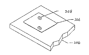
FIG. 2A shows a perspective view of a sensor electrode
printed irectly
d on an
instrument
case;
FIG. 2B shows a cross-sectional view of a sensor
electrode printed directly on an instrument case;
FIG. 3 shows schematically a programmable gain
10amplifier using parallel implementation of a switched
a
resistor array;
FIG. 4 shows schematically a programmable gain
amplifier using series implementation of a switched
a
resistor array;
15FIG. 5 shows an embodiment of an amplitude comparison
element;
FIG. 6 shows another embodiment of an amplitude
compariso n element;
and
FIG. 7 shows a flowchart illustrating a method for
20detecting an energized
electric
conductor.
Use of the
same
reference
numbers
in different
figures
indicates similar or like elements.
DETAILED DESCRIPTION
25 The following description is meant to be illustrative
only and not limiting. Other embodiments of this invention
will be apparent in view of the following description to
those skilled in the art.
FIG. 1 illustrates a block diagram of an AC measurement
30 system 100 which includes an electric field sensor 102 for
detecting an AC signal emanating from a concealed energized
electric conductor. The resulting AC signal on line 104
indicating detection is amplified by a programmable gain
amplifier 106. The amplified signal on line 108 is measured
35 by an amplitude comparison element 110. A digital signal on
line 112 indicates whether or not the signal exceeds the
reference level set up the microprocessor 114 on the
amplitude reference control line 120. Microprocessor 114
5
CA 02346141 2001-03-30
WO 01/09635 PCT/US00/21179
then uses the amplitude information to set the amplifier
gain for programmable gain amplifier 106 over a gain control
line 122 and controls the amplitude comparison element 110
over an amplitude reference control line 120.
S ("Microprocessor" here generally refers to a microprocessor,
micro-controller, or equivalent controller device.) In one
embodiment, amplitude reference control line 120 is a single
line for a pulse width modulator. In another embodiment,
amplitude reference control line 120 is a bus including
several lines when amplitude reference control line 120
controls a digital to analog converter (DAC). Gain control
line 122 is typically actually a bus. Microprocessor 114
controls programmable gain amplifier arid amplitude
comparison element 110 as discussed in detail below. In one
embodiment, microprocessor 114 also controls a display 118
which displays the resulting information over a display
control line 116. Display 118 may be e.g., audible, using a
beeper, or visual, using LEDs or a liquid crystal display.
Microprocessor is, for example, a Microchip PIC 16C54
programmed to carry out the functionality disclosed herein;
such programming is well within the skill of one of ordinary
skill in the art.
FIGS. 2A and 2B show a perspective view and a cross-
sectional view, respectively, of a sensor electrode printed
directly on an instrument case. Electric field sensor 102
has a sensor electrode 204 directly printed on an inside
bottom panel of instrument case 206. Sensor electrode 204
is of a conventional conductive ink. Sensor electrode 204
interconnects to the associated circuitry on a printed
circuit board 202 at the elevated contact areas ("mesas")
208 formed on the inside bottom panel of instrument case
206. This interconnection takes place when the instrument
is assembled. Sensor electrode 204 advantageously
eliminates the air gap between the electrode and the
instrument case in a conventional electric field sensing
instrument, thereby increasing sensitivity.
FIGs. 3 and 4 show schematically two embodiments of
programmable gain amplifier 106. Programmable gain
6
CA 02346141 2001-03-30
WO 01/09635 PCTNS00/21179
amplifier 206 provides the required dynamic range, typically
about 20 to 30 dB, for measurement of background electric
field. In one embodiment, a logarithmically programmed gain
amplifier is used. A logarithmically programmed gain
amplifier is desirable in AC detection because when the
dynamic range is large, e.g., >20 dB, a logarithmically
programmed gain amplifier provides equal step sizes
regardless of signal amplitude. In addition, in AC signal
detection, the sensor electrode is equivalent to a coupling
capacitor of a few picofarads. At 60 Hertz (the typical AC
frequency), a few picofarads is an extremely high impedance,
typically, more than 100 Megohms. Because the input signal
impedance is very high, the output signal of a fixed gain
amplifier is proportional to the input load resistor.
Therefore, in accordance with this invention, the
programmable gain amplifier includes a single fixed gain
amplifier and a switched resistor array coupled to an input
terminal of the fixed gain amplifier. Other types of
amplifier such as a linear gain amplifier may be used.
However, a linear gain amplifier requires additional steps
to maintain the output signal level within a particular
range.
FIG. 3 shows a programmable gain amplifier 106 using a
parallel implementation of a switched resistor array.
Capacitive field sensor 102 detects an AC signal and
provides in response an AC signal current on line 109 which
is coupled to a resistor array having resistors 310 through
317 coupled in parallel. The resistor array is also coupled
to an input terminal A of a fixed gain amplifier 308.
Typical resistor values for resistors 310 through 317 are
approximately 100 kilohms to approximately 3 megohms.
Typical gain for fixed gain amplifier 308 is 300 (50 dB).
AC signal current on line 104 is typically in the nano amp
range.
Each resistor 310 through 317 is controlled by a
corresponding switch 320 through 327 which is coupled in
series with the resistor. In one embodiment, each switch
320 through 327 consists several transistors as part of an
7
CA 02346141 2001-03-30
WO 01/09635 PCT/US00/21179
integrated circuit. In another embodiment, each switch 320
through 327 is a discrete transistor. In one embodiment,
resistors 310 through 317 are part of the integrated circuit
on a chip.
Each of the switches 320 through 327 in switch array
300 is in turn controlled by a gain control line 122 from
microprocessor 114 through a digital decoder (not shown).
Hence, depending on the position of each switch 320 through
327, the input load resistance of fixed gain amplifier 308
is modified, thereby changing the gain of programmable gain
amplifier 106. For example, for an eight step amplifier (6
dB per step) with a 256 to 1 range (48 dB) of selectable
gain, each resistor 310 through 317 has one half the
resistance of the resistor in the previous stage. This is
because the output signal (effectively, the gain) is
proportional to resistance. Therefore, cutting a resistor
in half cuts the output in half. It is noted that modifying
the input load resistance to a fixed gain amplifier is
simpler than modifying the gain of a variable gain amplifier
which requires additional circuitry.
Programmable gain amplifier 106 in accordance with the
present invention requires less board space than required by
a variable gain amplifier because variable gain amplifiers
are fairly complex, especially if gain variations are very
large. In addition, circuitry for meeting the stability
requirements is usually added when an analog system requires
continuous feedback to maintain a constant output level,
increasing the complexity and cost.
The same principle is applicable to a series
implementation of a switched resistor array. FIG. 4 shows
an alternative programmable gain amplifier using a series
implementation of a switched resistor array having resistors
410 through 417 coupled in series. In this embodiment,
capacitive field sensor 102 detects an input signal electric
field strength 104 and is coupled to a resistor array and an
input terminal A of a fixed gain amplifier 408. Typical
resistor values for resistors 411 through 417 are
approximately 100 kilohms to approximately 3 megohms.
CA 02346141 2001-03-30
WO 01/09635 PCT/US00/21179
Typical gain for fixed gain amplifier 408 is 300 or 50 dB.
Each resistor 411 through 417 is controlled by a
corresponding switch 921 through 427 coupled in parallel
with the resistor. Each switch 421 through 427 in switch
array 400 is controlled by a gain control line 122 from
microprocessor 114 through a digital decoder (not shown).
Similar to the parallel implementation of programmable gain
amplifier discussed above, the switch positions of switches
421 through 427 determine the input load resistance of fixed
gain amplifier 408 which in turn determine the gain
characteristic of programmable amplifier 106. The
structures shown in FIGS. 3 and 4 can be used in a custom
integrated circuit to provide excellent accuracy with
minimum use of area, hence low cost.
FIG. 5 illustrates schematically an embodiment of the
amplitude comparison element 110 of FIG. 1. An amplified AC
signal (ACIN) on line 108 is compared to a reference value
(THRESHOLD VOLTAGE) on line 502 by a comparator 504. The
reference value on line 502 is controlled by microprocessor
114 through a pulse-width modulator (PWM) 510.
Microprocessor 114 generates a variable duty cycle pulse
train signal (PWM OUT) on amplitude reference control line
120. The PWM filter 510 removes the AC component of the
pulse train, leaving only a DC level, the threshold voltage
502. The filtered amplitude reference control signal on
amplitude reference control line 120, i.e., the reference
value on line 502, is then used for the comparison.
If the peak amplitude of the amplified AC signal on
line 108 exceeds the reference value on line 502, comparator
504 changes the state of output signal on line 505 which
sets a flip-flop 506. Flip-flop 506 is therefore used as a
memory element to store the information that output signal
on line 505 has changed state. Flip-flop 506 is reset by a
reset signal on line 508 from microprocessor 119.
In one embodiment, flip-flop 506 is an "SR" flip-flop
having a pair of input terminals SET and RESET. After a
momentary RESET, the flip-flop output will be low unless a
subsequent SET input is received. If a subsequent SET input
9
CA 02346141 2001-03-30
WO 01/09635 PCT/US00/21179
is received, the flip-flop stores this information until
another RESET is received. By utilizing flip-flop 506 as a
storage element, a peak AC signal can be detected. Because
the flip-flop performs the peak detection function,
microprocessor 114 can perform other functions during the
intervening time, the other functions being, e.g.,
automatically measuring parameters such as time intervals,
rise and fall times and frequency.
PWM filter 510 is relatively slow and requires a
waiting period when an input value, i.e., PWM OUT, from
microprocessor 114 changes, to allow the DC voltage to
settle to the new value. Hence, while a PWM provides high
resolution, it may not be fast enough for some applications.
FIG. 6 shows an alternate embodiment of amplitude
comparison element 110. In this embodiment, a digital to
analog converter (DAC) 610 is used to increase the speed of
the conversion operation. Microprocessor 114 varies the
threshold rapidly enough to monitor the amplitude of
amplified AC signal on line 108 as it varies (e. g., every
100 microseconds).
A tracking process rapidly measures the instantaneous
amplitude of the amplified AC signal on line 108. The
tracking process sets the value of DAC 610, then observes
whether comparator 604 is high or low. If the output signal
of comparator 604 is high, the value of the amplified AC
input signal on line 108 is larger than the reference value
(THRESHOLD VOLTAGE) on line 602 and the output signal for
DAC 610 is increased 1 step. Similarly, if the output
signal from comparator 604 is low, the value of the
amplified AC input signal on line 108 is less than the
reference value on line 602 and the output of DAC 610 is
decreased one step. This process is repeated continuously,
resulting in the output of DAC 610 continuously tracking the
amplitude of the amplified AC input signal on line 108. By
monitoring the output value of DAC 610, microprocessor 114
can observe the changes in direction which occurs as the
signal passes through a maximum or minimum peak.
CA 02346141 2001-03-30
WO 01/09635 PCT/US00/21179
In the previous example, discussed in reference to FIG.
5, an entire period of the input frequency is required for
one comparison. Hence, to measure the amplitude to a 1 bit
resolution of an 8 bit system requires 8 periods or about
150 milliseconds. The tracking process, on the other hand,
allows the same resolution in 1/2 cycle, since the
instantaneous amplitude is determined and either the minimum
or the maximum is determined as soon as the signal value
achieves one or the other.
In one embodiment, the instrument is automatically
recalibrated when the original calibration is performed at
or near the point of maximum electric field, i.e., the
instrument is very near or directly over the_concealed
conductor. Without recalibration, the instrument may fail
to detect a hidden electric conductor since calibration
occurred at the point of maximum signal, and no larger
signal will be found. In one embodiment, as the instrument
moves away from the concealed conductor, the electric field
level decreases and when there is a sufficient decrease, the
instrument recalibrates and alerts the user that the
instrument is moving away from the concealed conductor by
either a visual display or an audible indication. When the
user returns the instrument to the original location where
the first calibration occurred, the electric field would
have increased sufficiently compared to the new calibration
to trigger an indication indicating the presence of a
concealed conductor.
"Homing in" on a electrical conductor is possible by
successively recalibrating the unit. In one embodiment, the
recalibration is triggered by the user pressing a reset
button coupled to the microprocessor. In another
embodiment, the recalibration is triggered by the user
turning off and on the power to the instrument. When the
original calibration is done at a location far from the
conductor, the indication of the presence of the energized
electric conductor is given over a large area. By
recalibrating successively closer, the indicated area
decreases until the electric energized conductor is closely
11
CA 02346141 2001-03-30
WO 01/09635 PCT/US00/21179
located.
FIG. 7 shows in a flowchart a process carried out by
the above-described AC measurement system 100. The process
starts in step 700 when a user turns on the instrument or
presses a reset button. The process starts a calibration
process in the microprocessor by first determining a
background electric field level at the starting location
(step 702). This background electric field level is then
used as a reference value for the measured electric field
from other locations.
The user moves the instrument over an area, such as a
wall, to locate a concealed electric energized conductor.
The electric field strength is measured at a new location
(step 704). The ratio between the background signal level
and the electric field strength measured at the new location
is calculated (step 706). Ratios is calculated (rather than
only subtraction) for the comparison because detection
requires the measurement of a small change in electric field
level as compared to a large background signal. The actual
change in electric field level for a given movement toward
or away from the concealed electric conductor is
proportional to the level of the background field.
Therefore, a ratio gives a constant sensitivity. That is,
the change in ratio for a given movement of the sensor is
constant. If a difference measurement other than a ratio is
used, the sensitivity of the unit would depend on the
magnitude of the background signal.
Next, the process determines whether the ratio is less
than an empirically predetermined value, e.g., approximately
0.8 (step 708). If the process determines that the ratio is
less than or equal to the predetermined value, the
instrument is automatically recalibrated (step 710). A new
reference level, i.e., a new background signal level, is
generated in this step. The process returns to step 704 and
continues.
If the process determines that the ratio is not less
than the predetermined value, the process determines whether
the ratio is greater than a predetermined value, e.g., 1.2
12
CA 02346141 2001-03-30
WO 01/09635 PCT/US00/21179
(step 724). Number 1.2 is selected because the optimal
ratio is approximately 1.18 (i.e., 18a increase) which is an
empirically determined number. Tf the number is too low,
random variations due to wall conditions, such as a stud or
nail, can cause erroneous indications. On the other hand,
if the number is too high, the instrument may fail to find
the hidden conductor. If the ratio is greater than the
predetermined value, the process generates a signal
indicating that a concealed conductor is present (step 716).
The signal generated is, for example, a visual or an audible
indication. The process returns to step 704 and continually
repeats steps 704 through 716 until the instrument is turned
off or a reset switch is activated.
In one embodiment, a single LED having multifunction
modes (on, off, or blinking) provides an alert to the
presence of an AC signal. For example, a constant on LED
indicates the location of a concealed conductor; the off LED
indicates the absence of the concealed conductor; and an LED
blinking at a constant rate indicates the instrument was
calibrated near a the conductor. In one embodiment, the LED
blinks at varying rate to indicate whether the instrument is
getting closer or farther away from the conductor. For
example, an increasing rate indicates that the conductor is
getting closer and a decreasing rate indicates that it is
getting farther away. Similarly, an audible indicator can be
used to indicate the location and the presence or absence of
the concealed energized electric conductor with sounds of
varying frequencies.
Although the invention has been described with
reference to particular embodiments, this description is
illustrative and not limiting. Various other adaptations
and combinations of features of the embodiments disclosed
are within the scope of the invention as defined by the
following claims.
13