Note: Descriptions are shown in the official language in which they were submitted.
CA 02346283 2001-04-04
WO 00/21607 PCT/AU98/00846
1
HIGH COMPLIANCE OUTPUT STAGE FOR A TISSUE STIMULATOR
BACKGROUND OF THE INVENTION
Field Of The Invention
This invention pertains to a neural or muscular tissue stimulating
prosthesis capable of delivering a high current stimulation signal to a nerve,
or
brainstem, of a patient and, more particularly, to a cochlear prosthesis with
a
power supply having an output which can be selectively boosted to a high
level.
Description Of The Prior Art
Though the subject invention will find application with many types of
tissue stimulating device it will be described in relation primarily to
cochlear
prosthesis systems. These prostheses are used to provide therapy to patients
suffering from certain hearing impairing conditions. Frequently such systems
are of a "two-part" design in that they comprise two sections: an internal or
implanted section, and an external section. The external section includes a
microphone for receiving ambient sounds and converting them to electrical
signals. Power to the external section is provided by a battery. The
electrical
signals are processed and sent to the implanted section. The implanted section
then generates excitation signals to excite the aural nerve of the patient by
means of appropriately positioned stimulation electrodes.
~ Most commonly, the external section of a two-part cochlear prosthesis is
inductively coupled by a transcutaneous RF link to the implanted section. The
energy of the electrical signals in the RF frequency range is rectified and
stored
by a power supply located in the internal section. It is that power supply
which
provides the energy required to power the internal section and to generate the
stimulus signals.
More recently there has been a trend in cochiear prosthesis design
towards the use of totally implantable prostheses. In such devices the entire
cochlear prosthesis, including a battery, is implanted. Obviously it is highly
desirable that a totally implanted cochlear prosthesis be of as small a size
as
possible. In order to achieve the necessary miniaturisation it is important
that
the power supply, and so by necessity the battery, be of a small size.
CA 02346283 2001-04-04
WO 00/21607 PCT/AU98/00846
2
To minimise the power requirements of the implanted section of a
cochlear prosthesis, whether it be of the totally implanted or of the two-part
type,
it is desirable to operate it at as low a voltage as possible. One problem
however with this appraach is that a minimised voltage may present
difficulties
for the circuitry which is to apply the stimulation currents. In particular, a
low
operating voltage has hitherto reduced the maximum available amplitude of the
stimulating signals that may be generated. An undesirable result is that the
dynamic range of the stimulation signals conveyed to the patient is reduced so
that loud sounds are perceived by the patient as being quieter than they
should
be.
Another problem, which is relevant only to cochlear prostheses of the
two-part type, is that power supply voltage within the internal section is
sensitive
to the relative position and spacing of the coils used for the inductive
coupling of
the internal and external sections. When this positioning is not correct, the
inter-
coil coupling is not optimal, and therefore the available power in the
implanted
section drops resulting in a limitation of the amplitude of the stimulation
current
that can be generated into the electrodes.
The problem of insufficient power being available to deliver the
appropriate stimulations is especially acute for cochlear prostheses using
biphasic stimulation current pulses. These pulses consist of two consecutive
phases of opposite polarities with the first phase having a higher peak
voltage
amplitude than the second phase, due to the capacitive component of the toad.
If the power supply for the internal section has an inadequate voltage level
(i.e.,
the power supply has a compliance problem), the current during the first phase
of a pulse is smaller than required while the current during the second, lower
voltage phase, remains unchanged thereby resulting in an unbalanced
stimulation pulse.
In order to resolve these problems it has been proposed that, when
sufficiently high voltage levels are not available, the duration of the
biphasic
pulse be increased to compensate, sa that the charge delivered during each
current phase remains approximately constant. However, the use of longer
stimulation pulses inherently reduces the maximum stimulation rate of the
device and so is undesirable.
CA 02346283 2001-04-04
WO 00/21607 PCT/AU98/00846
3
OBJECTIVES AND SUMMARY OF THE INVENTION
In view of the above-named disadvantages of the prior art, it is an
objective of the present invention to provide a tissue stimulating system with
improved power supply in order to eliminate ~ non-compliant episodes, i.e.
episodes in which stimulation pulses are applied which are of less-than-
desired
current.
A further objective is to provide a tissue stimulating system which
selectively increases the voltage available to the stimulation electrodes to a
level sufficient to provide suitable cochlear stimulation.
Other objectives and advantages of the invention shall become apparent
from the following description.
In particular, a cochlear prosthesis system constructed in accordance with
this invention includes a means for receiving and processing ambient sounds to
generate processed signals which are applied to the aural nerve through an
electrode array. Importantly, the generation of the output signal being
delivered
to an electrode is monitored and if it is determined to be insufficient a
voltage
multiplier scheme is used to boost the voltage of the power supply to a high
level temporarily, thereby ensuring that the output current can reach the
required value.
According to a first aspect of the invention there is provided a tissue
stimulating system of the type wherein a power supply and at least one
programmable current source are provided for generating a stimulation current
of predetermined amplitude, said system further comprising
a booster circuit for selectively boosting the supply voltage of said power
supply when said supply voltage is insufficient to allow said current source
to
provide a predetermined stimulation current.
According to another aspect of the invention there is provided a cochlear
prosthesis system including:
a microphone for picking up ambient sounds;
signal processing circuitry coupled to the microphone for determining
stimulation signals corresponding to said ambient sounds;
CA 02346283 2001-04-04
WO 00/21607 PCT/AU98/00846
4
an electrode array for applying said stimulation signals to the nervous
system of a patient;
a power supply for providing energy for the generation of said stimulation
signals;
an energy storage device arranged and constructed to selectively
supplement said power supply;
a sensor for monitoring the generation of said stimulation signals to
determine if said power supply requires supplementation by said energy
storage device in order to enable generation of said determined stimulus
signals; and
a multiplier switching circuit for selectively switching said energy storage
device so that it supplements the voltage provided by the power supply in
order
to ensure that stimulation signals as determined by the signal processor are
generated.
Finally, according to yet another aspect of the invention there is provided
a method for improving the compliance of the stimulation current output stage
of
a tissue stimulating system, said output stage including at least one
programmable current source and power supply, said method including the
steps of
a) determining if the voltage across each said current source is sufficient to
allow generation of a stimulation current of desired amplitude;
b) in the event that said voltage is determined to be insufficient in step a),
placing a charged energy storage device in series with said power supply so as
to increase the potential voltage across each said programmable current
source.
BRIEF DESCRIPTION OF THE DRAWINGS
Figure 1A shows a block diagram of a prior art two-part cochlear
prosthesis system;
Figure 1 B shows a block diagram of a totally implanted cochlear
prosthesis system;
Figure 2 shows a block diagram of a prior art output stage of a two-part
cochlear prosthesis system;
CA 02346283 2001-04-04
WO 00/21607 PCT/AU98/00846
Figure 3 shows a block diagram of an output stage of a cochlear
prosthesis system, either of the two-part or totally implanted type,
constructed in
accordance with the present invention wherein the standby power supply is in
the idle mode;
5 Figure 4 shows a block diagram of the output stage of a cochlear
prosthesis system constructed in accordance with this invention wherein the
standby power supply is in the active mode to boost the primary power supply;
Figure 5 shows a pair of desired stimulation current waveforms, the
second waveform resulting in an otherwise non-compliant condition;
Figure 6 shows the current that is required to flow in the current source to
generate the desired stimulus current of Figure 5;
Figure 7 shows the corresponding voltages at nodes n1 and n2 of
Figures 3 and 4;
Figure 8 shows the corresponding voltage waveforms across the current
source;
Figure 9 shows a generalised block diagram of an embodiment of the
invention; and
Figure 10 shows an alternate embodiment of the invention.
Figure 11 depicts a further embodiment of the invention.
Figure 12 depicts a flowchart of the operation of the embodiment of
Figure 11 in one mode.
Figure 13 depicts a flowchart of the operation of the embodiment of
Figure 11 in another mode.
DETAILED DESCRIPTION OF THE INVENTION
Referring now to Figure 1A, an example of a tissue stimulating device
being a cochlear prosthesis is depicted. A cochlear prosthesis system 10 of
the
two-part type consists of an internal or implanted section 12 and an external
section 14. The external section 14 includes a microphone 16, a signal
processor 18, an encoder 20, and a data and pawer transmitter 23 as well as a
patient map memory 22 and external section power supply 24. Briefly, ambient
sounds are picked up by microphone 16 and sent to the signal processor 18.
CA 02346283 2001-04-04
WO 00/2160'7 PCT/AU98/00846
6
The signal processor detects various components from these sounds and
adjusts them according to patient map memory 22 which stores data concerning
the patient's perceptual response to stimulation by the cochlear prosthesis.
The
adjusted data is sent from signal processor 18 to data encoder 20. The encoder
converts the data from the signal processor into a serial stream of binary
data. A
radio frequency signal is amplitude modulated by this data in the power
transmitter 23 and transmitted via an RF link to the internal section 12. The
RF
link consists of two coupled coils 28,30.
In addition to coil 30, internal section 12 includes a tuning capacitor 32
and rectifier consisting of diode 36 and storage capacitor 34. Coil 30, tuning
capacitor 32, diode 36 and storage capacitor 34 comprise the power supply for
the internal section. The electrode array control circuitry 40 includes
electrode
switching control circuits 44 and a programmable current source 48. The data
decoder 38 receives the signal transmitted from coil 28 to coil 30 and sends
commands to the array control circuitry 40. In response, stimulation signals
are
applied by the control circuitry 40 to a cochlear electrode array 46. The
array 46
is disposed along the patient's basilar membrane (not shown). Except as noted
below, the operation of the system 10 is described in U.S. Patent No.
4,532,930,
the contents of which are incorporated herein by reference.
Referring now to Figure 1 B, therein is depicted a block diagram of a
totally implantable cochlear prosthesis. The operation of the prosthesis
depicted in Figure 1 B is largely analogous to that of the two-part device
shown
in Figure 1A, although, because there is no separation of the prosthesis into
external and internal sections the decoder, encoder, RF link and rectifier
circuitry
which appear in two-part designs are not needed. The modules shown in
Figure 1 B are highly similar to those of the device depicted in Figure 1 A
and
therefore the common elements have been identified by the same indicia. The
totally implantable prosthesis may be entirely powered by an implanted battery
power supply 24.
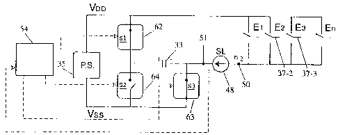
Referring now to Figure 2, there is depicted a typical prior art output
stage as used in two-part cochlear implants for delivering stimulation
signals.
CA 02346283 2001-04-04
WO 00/21607 PCT/AU98/00846
7
The arrangement of Figure 2 includes a plurality of conductors 37-1 to 37-n
and
electronic switches E1...En controlled by switching control 44. Each of the
switches E1...En are used to selectively connect one of the conductors 37-n of
array 46 to either Vdd or programmable current source 48. The programmable
current source 48 is additionally under command of switching control 44 which
sets the amplitude of the stimulations to be generated. Power supply 35
comprises either a tuned circuit, rectifying diode and storage capacitor, as
described with reference to Figure 1 in the case of a two-part prosthesis, or
a
battery and associated circuitry in the case of a totally implantable cochlear
prosthesis.
In order to deliver a stimulation pulse via conductor 37-2, for example, the
corresponding switch E2 is set to a first position wherein the conductor 37-2
is
connected to the positive rail Vdd. The return path is established through one
of
the other conductors, such as 37-3 in which case the switch E3 is set so that
it is
now connected to the programmable current source 48. The current source 48
is set by switching control 44 as discussed above.
Current source 48 is set so that currents of a specified amplitude are
passed through the selected electrodes. After a predetermined time the two
switches E2, E3 are flipped to the opposite connection thereby reversing their
connections to the Vdd rail and current source 48 and in consequence
completing the delivery of a biphasic current stimulus pulse through the
tissue.
It should be noted that although the direction of current through the tissue
is
reversed, the direction of current out of current source 48 remains constant.
As discussed above, one problem with this arrangement is that under
certain conditions the voltage across power supply 35 may be insufficient to
allow the proper operation of current source 48. With reference to Figure 2,
if
the voltage across source 48 falls too low then it will not be possible to
attain
high current amplitudes. This situation may occur for example when the tissue
to be stimulated presents a higher than usual impedance or when it is desired
to
present an unusually high stimulation. In either case, the potential
difference
across current source 48 will no longer be sufficient for satisfactory
operation of
the source. Consequently a non-compliance condition will result. Figures 3 and
4 show an improved circuit which remedies this problem.
CA 02346283 2001-04-04
WO 00/Z1607 PCT/AU98/00846
8
Figures 3 and 4 include components necessary for the implementation of
the present invention in a first embodiment, being multiplier switches S1, S2
and S3, labelled 62, 64 and 63, sensing and multiplier switch control circuit
54
and a standby multiplier capacitor C1, 33. It will be noted that by closing
multiplier switches 62 and 63 as shown in Figure 3 the standby multiplier
capacitor 33 is placed in parallel with the power supply 35 and in that
position
will become charged. Furthermore by opening switches S1 and S3 and closing
switch S2, as shown in Figure 4, capacitor 33 is placed in series with the
power
supply 34 so that the potential difference between node n1, 51 and power rail
Vdd is greatly increased. Multiplier control circuit 54 may be implemented
using
digital logic, alternatively it may be implemented as software running on an
implanted microprocessor.
The operation of the circuit of figures 3 and 4 shall now be described in
conjunction with the waveshapes of Figures 5-8. Figure 5 depicts the plurality
of
current waveforms 70 and 73 requested by the switching control 44 to be
passed through the load by programmable current source 48. It can be seen
that each wavefarm is biphasic, consisting of two current pulses of equal
amplitude and opposite polarity. Thus, lower amplitude biphasic current
waveform 70 consists of positive and negative pulses 71 and 72 respectively,
and higher amplitude current waveform 73 consists of positive and negative
pulses 74 and 75.
Next, Figure 6 depicts the corresponding current waveforms that must
pass through the controlled current source 48 to produce the desired
stimulation
current waveforms 70 and 73. The current source must pass two lower
amplitude square waves 76 and 77 to generate stimulus pulses 71 and 72
respectively, and two larger amplitude square waves 78 and 79 to generate the
stimulus pulses 74 and 75. The current pulse 78 exceeds the capability of the
power supply and necessitates a boost, as will be described. In the specific
embodiment shown in Figure 4, this boost is provided by a voltage multiplier
as
follows:
CA 02346283 2001-04-04
WO 00/21607 PCT/AU98/00846
9
Referring to Figure 7 the voltage waveform 80 at node n2 is depicted
measured with reference to Vss; and the voltage waveform 88 at node n1 is
depicted also measured with respect to Vss. It can be seen from the shape of
the voltage waveform 80 that the load contains a capacitive component. The
level Vc marks the minimum voltage across the current source 48 (measured as
the voltage at n2 with respect to Vss) at which compliance with the desired
current waveform of Figure 6 can be maintained. The voltage Vca is a little
higher than Vc and is the trigger control voltage at which a voltage
compliance
alarm is sensed and voltage multiplier action is commenced. At 85 of the graph
in Figure 7 the voltage 80 at n2 reaches the trigger control voltage Vca. This
condition is sensed and, very shortly after, switches 62 and 63 are opened and
switch 64 is closed. The reconfiguration of the switches has the effect of
placing
capacitor C1 between the current source 48 and Vss, consequently pulling the
voltage 88 at n1 down to a potential Vdd below Vss. This excursion of the
voltage 88 at n1 is shown as the waveform 89 in Figure 7. After its initial
drop at
85 the voltage 88 on n1 subsequently slowly decays towards Vss.
In Figure 8 the graph depicted shows the voltage waveform levels
measured at n2 with respect to n1. With reference to Figure 8 it is seen that
the
voltage level across the current source 48 is significantly increased at time
85
and consequently the current compliance margin is increased from the one
shown at 92, approaching the voltage compliance limit 86, to the substantial
margin 93.
At the completion of the first of the large amplitude pulses 83, switches S1
and S3 are again closed and S2 opened. They remain in that state until
another non-compliance state is detected.
Figure 9 depicts a generalised block diagram of an embodiment of the
invention. In this figure a power supply 100 maintains a power rail 102 at a
substantially constant voltage Vdd. A settable current source S~ 106 sets the
current which flows through the load. In standard operation the current flows
through a voltage booster 108 which is internally connected to the low
potential
rail Vss 110. The voltage Va at point or node 112 is sensed by a compliance
sensor 104, which compares the same to a settable trigger control voltage.
CA 02346283 2001-04-04
W4 00/21607 PCT/AU98/00846
Should the voltage across the load decrease so that Va falls below the trigger
voltage then the compliance sensar will set the compliance latch 109 which
will
activate the voltage booster 108. The booster pulls down the voltage at point
B
below Vss so that the potential difference across the current source S~, 106,
is
5 increased thereby ensuring the satisfactory operation of the current source
and
the maintenance of the desired current through the load. It will be realised
by
those skilled in the art that other arrangements are also possible, for
example a
re-arrangement of the circuit would make it possible to increase the potential
difference across the current source by raising the positive supply with
respect
10 to Vdd rather than lowering the negative supply with respect to Vss.
Figure 10 shows an implementation of the arrangement depicted in
Figures 2 and 4 and therefore the common elements have been identified by the
same indicia. In this embodiment, the sensor and control circuit 54 consists
of a
current source S~, (of much lower amplitude than S~) inverters U3, U4, a FET
switch Q1 and two NOR gates U1, U2 connected to form a standard flip-flop
latch. The trigger control voltage is provided at the gate of the FET Q1 and
its
source is used to monitor the voltage at n2, as shown.
Circuit 54 is designed so that when the voltage at n2 falls below a level
set by the trigger voltage on the gate of Q1 then the FET Q1 is turned on and
the
input to U3 falls low. Consequently, the latch formed by U2 and U 1 is set and
its
output goes high. When the output of the latch goes high switch S2 closes and
switches S1 and S3 are opened via inverter U4. This operation places C1 in
series with the current source S~ which has the effect of pulling the voltage
at
n 1, the negative end of current source S~, down and so prevents S~ from
entering a non-compliance state. C1 remains so connected until the end of the
stimulation phase at which time the reset input on U2 is set high, switches S1
and S3 close and switch S2 opens. The capacitor C 1 is then placed in parallel
with the power supply capacitor and recharged. The trigger control voltage
(which should be set to the compliance alarm voltage Vca plus the turn on
voltage of Q1 ) can be set by any stable reference voltage e.g., a diode-
configured FET or a band-gap reference.
CA 02346283 2001-04-04
WO 00/21607 PCT/AU98/00846
11
In the illustrated embodiment the power supply voltage in the internal
section is boosted simply and efficiently thereby ensuring that sufficient
energy
is provided to deliver proper stimulation to the electrodes in a short period
of
time so that adequate charge is delivered without the need to increase the
duration of the stimulation pulses. Moreover, this boosting occurs only when
it is
required. At all other times a lower voltage is provided thereby reducing the
overall power consumption of the system. The switches S1-S3 can be
manufactured using a modern CMOS IC technology so that the delay in
boosting the voltage can be only a few microseconds or less.
Referring now to Figure 11 there is depicted a further embodiment of the
invention in which the voltage doubter is activated under command of a
compliance calculator. The compliance calculator takes its input from analog
to
digital converter 131 which is coupled to differential amplifier 134.
Differential
amplifier 134 determines the voltage Vn drop across the electrode - tissue
combination, represented by load 107, of a particular electrode. Given this
value of voltage drop, for a current stimulus of particular amplitude, the
impedance of the load is readily calculated by compliance calculator 130.
Referring now to Figure 12 the determination of the threshold current for
each electrode by compliance calculator 130 will be explained. This procedure
may be performed by the microprocessor that performs the signal processing
tasks of the prosthesis or alternatively by a maths co-processor operating
under
the command of the signal processing microprocessor.
At box 146 the electrode counter variable n is initialised to 1. At box 148
a known current stimulus lest is applied via the nth electrode. At box 150 the
voltage Vn across the load 107 is measured by differential amplifier 134 and
converted to a digital value, by ADC 131, which is coupled to compliance
calculator 130. At box 152 compliance calculator 130 calculates the load
impedance for the nth electrode as Zn= Vn/I~est. The compliance threshold
current for the nth electrode, In,t is then calculated as I",t = Vmax/Zn where
Vmax
is the maximum voltage that can be provided across the current source without
the aid of voltage boosting. At decision box 156 the electrode counter
variable n
is tested to see if the calculation procedure has been performed for all of
the
CA 02346283 2001-04-04
WO 00/21607 PCT/AU98/00846
12
electrodes. If it has not been so performed then n is incremented at box 154
and
the entire procedure repeated for the next electrode until a compliance
threshold current has been determined and stored for all of the electrodes.
Referring now to Figure 13 the further operation of the device of Figure 11
will be explained. At box 136 the controlling microprocessor, for example the
same microprocessor that implements signal processor 18 of Figure 1 B,
determines the intensity of the next stimulus current IS and the electrode n
via
which the stimulus will be delivered.
At decision box 138 the amplitude of IS is tested to determine if it exceeds
the precalculated compliance threshold current for the electrode in question,
minus an operational margin, If the result of the test at 138 is positive then
the
need for voltage boosting is indicated. Control then diverts to box 140
wherein
the compliance latch 140 is set so that voltage booster 108 is placed into
service. The stimulus is then applied at box 142 and the compliance latch
reset
subsequent to delivery of stimulus at box 144.
Alternatively, if the result of the test at 138 is negative then no
requirement for voltage boosting is indicated and the system proceeds through
boxes 142 and 144 without setting the compliance latch.
Although the invention has been described with reference to several
particular embodiments, it is to be understood that these embodiments are
merely illustrative of the application of the principles of the invention.
Accordingly, the embodiments described in particular should be considered
exemplary, not limiting, with respect to the following claims.