Note: Descriptions are shown in the official language in which they were submitted.
CA 02346593 2001-05-08
FP00-0328-00
TITLE OF THE INVENTION
OPTICAL WAVEGUIDE DEVICES AND METHODS OF
FABRICATING THE SAME
BACKGROUND OF THE INVENTION
Field of the Invention
The present invention relates to optical
waveguide devices incorporating a planar optical
waveguide and methods of fabricating the same.
Related Background Art
The optical waveguide devices are optical devices
with an optical waveguide formed on a substrate, and
principal materials thereof are silica glass and
silicon. These materials expand or contract with
change in temperature and also vary their refractive
indices. In consequence, the optical path length of
the optical waveguide changes in the optical waveguide
device and the effective refractive index of the
optical waveguide also changes, thereby leading to
variation in optical characteristics.
The conventional, optical waveguide devices were
thus equipped with a temperature control system to keep
the temperature of the devices themselves constant so
as to maintain the optical characteristics thereof
constant. This temperature control system is composed,
for example, of at least a thermometer, a Peltier
device, and a control unit. Namely, in the temperature
I 1
CA 02346593 2001-05-08
FP00-0328-00
control system of this type, the control unit controls
the Peltier device to heat or cool the optical
waveguide device so that the temperature of the optical
waveguide device itself, measured by the thermometer,
is kept constant.
SUMMARY OF THE INVENTION
The inventors investigated the prior arts as
described above and found the following problem as a
result. The problem was that the temperature control
system in the conventional, optical waveguide devices
also required a power supply and other elements, in
addition to the thermometer, Peltier device, and
control unit, and the waveguide devices inevitably
became large in size.
The present invention has been accomplished in
order to solve the above problem and an object of the
present invention is to provide optical waveguide
devices having a structure of effectively suppressing
the variation in optical characteristics due to
temperature change without causing increase in the
device size, and methods of fabricating the waveguide
devices.
An optical waveguide device according to the
present invention comprises at least a first main
member having a positive coefficient of linear
expansion and a first sub member having a negative
2
CA 02346593 2001-05-08
FP00-0328-00
coefficient of linear expansion. The first main member
has a first major surface and a second major surface
opposing the first major surface and a core functioning
as an optical waveguide is disposed between these first
and second major surfaces. On the other hand, the
foregoing sub member is fixed to the first surface of
the first main member while covering the entire first
major surface of the foregoing first main member.
In the optical waveguide device having the
structure as described above, with increase in
temperature thereof (e.g., surface temperature), the
first main member having the positive coefficient of
linear expansion becomes about to expand, while the
first sub member having the negative coefficient of
linear expansion becomes about to contract. On this
occasion, the optical waveguide in the first main
member becomes about to prolong its path length because
of the expansion of the first main member, while
receiving compressive stress from the first sub member
because of the contraction thereof. The direction of
this compressive stress is parallel to the border
between the first main member and the first sub member.
Utilization of this difference between the material
properties successfully suppresses the variation in the
optical characteristics of the optical waveguide in the
optical waveguide device due to the temperature change.
3
CA 02346593 2001-05-08
FP00-0328-00
When the respective linear expansion coefficients of
the first main member and first sub member and the
respective thicknesses of the first main member and
first sub member are properly set, the temperature
dependence of optical characteristics of the optical
waveguide in the optical waveguide device can be
relaxed to a practically negligible level. Since the
optical waveguide device can be realized in structure
in which the first main member and the first sub member
are cemented together, or in structure in which the
first main member is directly formed on the first sub
member, the size thereof becomes extremely small.
The optical waveguide is normally formed on a
substrate, and in the present invention a part of the
first main member (e.g., an undercladding), or the
first sub member may be the substrate.
The optical waveguide device according to the
present invention may have a structure in which sub
members having a negative coefficient of linear
expansion covers both the first and second major
surfaces of the first main member. Namely, the optical
waveguide device may comprise a second sub member
located so as to sandwich the first main member between
the first sub member and the second sub member. In
this case, the second sub member has the negative
coefficient of linear expansion and is provided
4
CA 02346593 2001-05-08
FP00-0328-00
directly or through an adhesive on the second major
surface while covering the entire second major surface
of the first main member. Further, the optical
waveguide device according to the present invention may
comprise a second main member located so as to sandwich
the first sub member between the first main member and
the second main member. This second main member has a
positive coefficient of linear expansion and is
provided directly or through an adhesive on the first
sub member while covering an entire major surface
thereof opposite to a major surface facing the first
major surface of the first main member. In addition,
the optical waveguide device according to the present
invention may further comprise a third sub member
provided directly or through an adhesive on a side face
of the first main member, located between the first and
second major surfaces, while covering the entire side
face. This third sub member has a negative coefficient
of linear expansion.
In these cases, the optical waveguide device can
be prevented from warping even with change in the
temperature of the optical waveguide device itself.
Particularly, in the structure wherein the third sub
member is fixed around the first main member, even if
the optical waveguide device itself changes its
temperature because of change in the ambient
5
CA 02346593 2001-05-08
FP00-0328-00
temperature or the like, the stress on the optical
waveguide device will be isotropic on the plane normal
to the optical axis of the optical waveguide, thereby
effectively suppressing increase in polarization
dependence of the optical waveguide in the optical
waveguide device.
The optical waveguide device according to the
present invention may also comprise a pressure applying
structure for applying pressure increasing in
proportion to a rise of temperature, in the direction
normal to each of the first and second major surfaces
of the first main member, in addition to the above
various structures. Particularly, the pressure
applying structure preferably comprises an insert
member having a positive coefficient of linear
expansion, and a clamping member for clamping the first
main member, sub member, and insert member in the
direction normal to each of the first and second major
surfaces. This clamping member has a positive
coefficient of linear expansion smaller than the linear
expansion coefficient of the insert member. In this
case, with increase in the temperature of the optical
waveguide device itself, expansion of the first main
member and contraction of the first sub member causes
the optical waveguide in the first main member to be
subject to compressive stress in the direction parallel
6
CA 02346593 2001-05-08
FP00-0328-00
to the first and second major surfaces. In addition
thereto, with increase in the temperature of the
optical waveguide device itself, the optical waveguide
in the first main member is also subject to compressive
stress in the direction normal to the first and second
major surfaces, because thermal expansion of the insert
member is greater than that of the clamping member. In
this way, the optical waveguide device is reduced in
anisotropy of compressive stress on the optical
waveguide, so as to decrease the birefringence of the
optical waveguide and thus effectively relax the
polarization dependence.
The optical waveguide devices having the
structures as described above (the optical waveguide
devices according to the present invention) are
fabricated by cementing the main member (first main
member) and the sub member (first sub member) of the
structure as described, together. In this fabrication
method, first, the main member having a positive
coefficient of linear expansion is prepared, the sub
member having a negative coefficient of linear
expansion is cemented to one major surface of the main
member, and another major surface of the main member is
polished or etched. The main member has a first major
surface and a second major surface opposing the first
major surface and incorporates an optical waveguide
7
CA 02346593 2008-03-14
located between the first and second major surfaces.
In another fabrication method capable of
fabricating the optical waveguide devices having the
structures as described above, a sub member having a
negative coefficient of linear expansion is prepared,
and a main member incorporating an optical waveguide is
formed on this sub member by a low-temperature CVD
method.
These fabrication methods both are suitable for
fabrication of the optical waveguide devices having the
structures as described above (the optical waveguide
devices according to the present invention). In
general, an absolute value of the linear expansion
coefficient of the main member is larger than that of
the sub member. However, since the thickness of the
main member itself can be made thinner by cementing the
sub member to one major surface of the main member and
thereafter polishing or etching the other major surface
of the main member,.the temperature dependence of
optical characteristics of the optical waveguide in the
optical waveguide device can be relieved-to the
practically negligible level. Since the thickness of
the main member can be made thinner by forming the main
member on the sub member by the low-temperature CVD
method, the same effect can be achieved thereby.
8
CA 02346593 2008-12-17
According to an aspect of the present invention there
is provided an optical waveguide device comprising:
a first main member having a first major surface and a
second major surface opposing said first major surface,
and incorporating an optical waveguide located between
said first and second major surfaces, said first main
member having a positive coefficient of linear expansion;
a sub member fixed to said first major surface while
covering the whole of said first major surface of said
first main member, said sub member having a negative
coefficient of linear expansion; and
a second main member located so as to sandwich said sub
member between said first main member and said second main
member, wherein said second main member has a positive
coefficient of linear expansion and is fixed to said sub
member while covering the whole of a major surface
opposing a major surface facing said first major surface
of said first main member, wherein said first and second
main members are different from each other in at least one
of materials and thicknesses thereof.
According to another aspect of the present invention
there is provided a method of fabricating an optical
waveguide device as described hereinabove, said method
comprising the steps of:
preparing a sub member having a negative coefficient of
linear expansion;
forming a first main member having a first major surface
and a second major surface opposing said first major
surface and incorporating an optical waveguide located
between said first and second major surfaces, on said sub
member by a low-temperature CVD method, said first main
8a
CA 02346593 2008-12-17
member having a positive coefficient of linear expansion;
and
forming a second main member on said sub member by a
low-temperature CVD method so as to sandwich said sub
member together with said first main member, said second
main member having a positive coefficient of linear
expansion, wherein the materials and thicknesses of said
sub member, said first main member, and said second main
member are adjusted so as to effectively suppress the
occurrence of warpage with temperature change and the
occurrence of change in the optical path length of said
optical waveguide.
The present invention will be more fully
8b
CA 02346593 2001-05-08
FP00-0328-00
understood from the detailed description given
hereinbelow and the accompanying drawings, which are
given by way of illustration only and are not to be
considered as limiting the present invention.
Further scope of applicability of the present
invention will become apparent from the detailed
description given hereinafter. However, it should be
understood that the detailed description and specific
examples, while indicating preferred embodiments of the
invention, are given by way of illustration only, since
various changes and modifications within the spirit and
scope of the invention will be apparent to those
skilled in the art from this detailed description.
BRIEF DESCRIPTION OF THE DRAWINGS
Fig. 1 is a drawing showing the structure of the
first embodiment of the optical waveguide device
according to the present invention.
Figs. 2A to 2C are views for explaining
fabrication steps of the optical waveguide device in
the first embodiment shown in Fig. 1.
Fig. 3 is a drawing showing the structure of the
second embodiment of the optical waveguide device
according to the present invention.
Fig. 4 is a drawing showing the structure of the
third embodiment of the optical waveguide device
according to the present invention.
9
CA 02346593 2001-05-08
FPOO-0328-00
Fig. 5 is a drawing showing the structure of the
fourth embodiment of the optical waveguide device
according to the present invention.
Figs. 6A to 6D are views for explaining
fabrication and packaging steps of the optical
waveguide device according to the fifth embodiment.
Fig. 7 is a view for explaining part of the
packaging step common to application examples of the
optical waveguide device according to the fifth
embodiment.
Fig. 8 is a view showing the cross-sectional
structure of the optical waveguide device according to
the fifth embodiment, as cut along line II-II shown in
Fig. 6C.
Fig. 9 is a view showing the cross-sectional
structure of a first application example of the optical
waveguide device (fifth embodiment) shown in Fig. 8.
Fig. 10 is a view showing the cross-sectional
structure of a second application example of the
optical waveguide device (fifth embodiment) shown in
Fig. 8.
Fig. 11 is a view showing the cross-sectional
structure of a third application example of the optical
waveguide device (fifth embodiment) shown in Fig. 8.
DESCRIPTION OF THE PREFERRED EMBODIMENTS
The embodiments of the optical waveguide devices
CA 02346593 2001-05-08
FP00-0328-00
according to the present invention will be described
along with their fabrication methods, referring to Figs.
1, 2A to 2C, 3 to 5, 6A to 6D, and 7 to 11. In the
description of the drawings the same elements will be
denoted by the same reference symbols and redundant
description will be omitted.
(First Embodiment)
The first embodiment of the optical waveguide
device and the fabrication method thereof according to
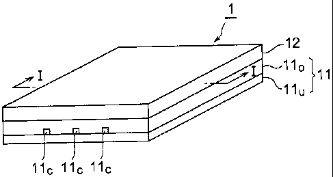
the present invention will be described first. Fig. 1
is a view showing the structure of the optical
waveguide device 1 according to the first embodiment.
This optical waveguide device 1 is provided with a
first main member 11 having a positive coefficient of
linear expansion and a sub member 12 having a negative
coefficient of linear expansion, which is fixed to the
first main member 11 so as to cover the whole of one
major surface of the first main member 11.
The first main member 11 consists of an
undercladding llu, cores 11, disposed on the
undercladding 11u, and an overcladding 11o disposed on
the undercladding 11u while covering the cores 11c. The
first main member 11 is made, for example, of a
principal material of silica glass or silicon and the
cores 11c are doped with a dopant, e.g., Ge02 for
raising the refractive index. The high-index cores 11c
11
CA 02346593 2001-05-08
FP00-0328-00
are surrounded by the low-index undercladding llu and
overcladding 110, and the cores 11c mainly function as
optical waveguides.
The sub member 12 is fixed to the upper surface
of the overcladding 11o in the first main member 11. A
suitable material for the sub member 12 is, for example,
porous glass having the linear expansion coefficient of
about -8 X 10⁻⁶/K, or crystallized glass having the
linear expansion coefficient of about -8 X 10⁻⁷ /K (e.g.,
Neoceram NO available from Nippon Electric Glass Co.,
Ltd).
Figs. 2A to 2C are views for explaining the
fabrication steps of the optical waveguide device 1 in
the first embodiment. Figs. 2A to 2C are illustrated
all corresponding to the cross section along line I-I
in Fig. 1.
In the first step, the undercladding 11u, cores
llc, and overcladding 110 are formed on a base or
substrate 11B by CVD (chemical vapor deposition), FHD
(Flame Hydrolysis Deposition), or the like (Fig. 2A).
Then the sub member 12 is cemented through an adhesive
to the upper surface of the overcladding 110 (Fig. 2B).
Here the adhesive is preferably one having high bond
strength for adhesion between glasses, particularly,
one resistant to shear stress and is suitably selected,
for example, from acrylic, epoxy, or phenolic adhesives.
12
CA 02346593 2001-05-08
FP00-0328-00
After that, the substrate 11B is removed by polishing
or etching (Fig. 2C). It is noted here that this
substrate 11B does not have to be removed completely.
The substrate 11B may remain in part. Through the
above steps, the optical waveguide device 1 of the
first embodiment is obtained.
The fabrication method of the optical waveguide
device 1 does not have to be limited to the above
method. For example, the optical waveguide device 1 of
the first embodiment can also be fabricated by
successively depositing the overcladding 110, cores 11c,
and undercladding 11u on the sub member 12 by the low-
temperature CVD method.
In this optical waveguide device 1 of the first
embodiment, with increase in the temperature thereof
(e.g., surface temperature), the first main member 11
having the positive linear expansion coefficient
becomes about to expand while the sub member 12 having
the negative linear expansion coefficient becomes about
to contract. As the temperature of the optical
waveguide device 1 itself increases in this way, the
optical waveguides in the first main member 11 become
about to prolong their path length because of the
expansion of the first main member 11. On the other
hand, the optical waveguides are subject to the
compressive stress due to the contraction of the sub
13
CA 02346593 2001-05-08
FP00-0328-00
member 12. The direction of this compressive stress is
the direction along the boundary surface between the
first main member 11 and the sub member 12.
Accordingly, even if there occurs change in the
temperature of the optical waveguide device 1 itself,
the optical characteristics of the optical waveguides
in the optical waveguide device 1 can be effectively
prevented from varying. When the respective linear
expansion coefficients of the first main member 11 and
sub member 12 and the respective thicknesses of the
first main member 11 and sub member 12 are properly set,
the temperature dependence of optical characteristics
of the optical waveguides in the optical waveguide
device 1 can be relieved to the practically negligible
level. Since the optical waveguide device 1 has the
cemented structure of the first main member 11 and the
sub member 12, the size thereof is sufficiently small,
as against the conventional devices.
(Second Embodiment)
The second embodiment of the optical waveguide
device according to the present invention will be
described below. Fig. 3 is a view showing the
structure of the optical waveguide device 2 according
to the second embodiment.
The optical waveguide device 2 of the second
embodiment is provided with a first main member 11
14
CA 02346593 2001-05-08
FP00-0328-00
having a positive coefficient of linear expansion,
which incorporates optical waveguides, a sub member 12
having a negative coefficient of linear expansion,
which is fixed to the first main member 11 so as to
cover the whole of one major surface of the first main
member 11, and another sub member 13 having a negative
coefficient of linear expansion, which is fixed to the
first main member 11 so as to cover the whole of the
other major surface of the first main member 11.
A material of the sub member 13 is selected in
much the same manner as the material of the sub member
12. The optical waveguide device 2 of the second
embodiment is fabricated by cementing the sub member 13
to the lower surface of the undercladding 11u of the
optical waveguide device 1 according to the first
embodiment. In other words, the optical waveguide
device 2 of the second embodiment has the laminated
structure in which the first main member 11 is
sandwiched between the sub members 12, 13.
The optical waveguide device 2 of the second
embodiment presents the effect similar to that achieved
by the optical waveguide device of the first embodiment,
and also provides the following effect. Namely, since
the device has the structure in which the sub member 12
is fixed to one major surface of the first main member
11 while the sub member 13 to the other major surface
CA 02346593 2001-05-08
FP00-0328-00
of the first main member 11, the optical waveguide
device 2 itself will be prevented from warping even if
there occurs change in the temperature of the optical
waveguide device 2 itself (e.g., surface temperature).
Particularly, when the sub members 12, 13 are made of
an identical material and in an equal thickness, the
optical waveguide device 2 is successfully prevented
from warping with temperature change.
(Third Embodiment)
The third embodiment of the optical waveguide
device according to the present invention will be
described below. Fig. 4 is a view showing the
structure of the optical waveguide device 3 according
to the third embodiment. The optical waveguide device
3 of the third embodiment is provided with a first main
member 11 having a positive coefficient of linear
expansion, which incorporates optical waveguides, a sub
member 12 having a negative coefficient of linear
expansion, which is placed on one major surface of the
first main member 11 and fixed so as to cover the
entire major surface, and a second main member 14
having a positive coefficient of linear expansion,
which is fixed to the sub member 12 so as to sandwich
the sub member 12 between the first main member 11 and
the second main member 14. The second main member 14
can be made, for example, of a principal material of
16
{
CA 02346593 2001-05-08
FP00-0328-00
silica glass or silicon, similar to the first main
member 11, or may be made of a metal material, e.g.,
aluminum.
The optical waveguide device 3 is fabricated by
fixing the second main member 14 onto the surface
opposite to the first main member 11, of the sub member
12 in the optical waveguide device 1 according to the
aforementioned first embodiment. When the second main
member 14 is made of the principal material of silica
glass, the second main member 14 is not deposited on
the sub member 12 by the FHD method, but by the low-
temperature CVD method. On the other hand, when the
second main member 14 is made of a metal material, the
second main member 14 is deposited on the sub member 12
by evaporation.
The optical waveguide device 3 provides the
effect similar to that achieved by the optical
waveguide device 1 of the aforementioned first
embodiment, and also provides the following effect.
Namely, the first main member 11 and the second main
member 14 are fixed to the respective major surfaces of
the sub member 12 opposing each other. This can
suppress the warpage of the optical waveguide device 3
even if there occurs change in the temperature of the
optical waveguide device 3 itself. Particularly, when
the first and second main members 11, 14 are made of an
17
CA 02346593 2001-05-08
FP00-0328-00
identical material and in an equal thickness, the
optical waveguide device 3 can be effectively prevented
from warping even with temperature change.
When the first and second main members 11, 14 are
made of their respective materials different from each
other, or in their respective thicknesses different
from each other, there is the possibility of warpage of
the optical waveguide device 3 with temperature change.
This will be discussed below.
Samples were prepared in common structure in
which the cross-sectional size of each core 11c was 6
,um X 6,um, intervals between the cores 11c were 28 ,um,
the thickness of the overcladding 11o was 0.03 mm, and
the thickness of the undercladding 11õ 0. The
thickness of the sub member 12 was 1.0 mm. The
principal material of the first main member 11 was
silica glass, the linear expansion coefficient of the
overcladding 110 0.70 X 10⁻⁶/K, and the linear
expansion coefficient of the cores 11c 0.97 X 10⁻⁶/K.
The principal material of the second main member 14 was
aluminum and the linear expansion coefficient thereof
X 10-6/K. Further, the principal material of the
sub member 12 was N-801 and the linear expansion
coefficient thereof -8.0 X 10⁻⁶/K.
25 The samples prepared were of three types; the
optical waveguide device without the second main member
18
CA 02346593 2001-05-08
FP00-0328-00
14 (Sample 1); the optical waveguide device in which
the thickness of the second main member 14 was set to
0.01 mm (Sample 2); and the optical waveguide device in
which the thickness of the second main member 14 was
set to 0.30 mm (Sample 3). The optical waveguide
device of Sample 1 corresponds to the optical waveguide
device 1 according to the foregoing first embodiment.
With increase in the temperature of the device
itself (e.g., surface temperature), Sample 1 warped in
convex shape on the side of the first main member 11
incorporating the optical waveguides, so as to prolong
the optical path length of the optical waveguides.
However, when the material having the linear expansion
coefficient of -9.0 X 10⁻⁶/K was applied to the sub
member 12, the warpage of Sample 1 due to the
temperature change was effectively suppressed and there
occurred no change in the optical path length of the
optical waveguides, either.
Sample 2 suffered from neither warpage nor change
of the optical path length of the optical waveguides
even with change in the temperature of the device
itself.
With increase in the temperature of the device
itself, Sample 3 warped in concave shape on the side of
the first main member 11 incorporating the optical
waveguides, so as to shorten the optical path length of
19
CA 02346593 2001-05-08
FPOO-0328-00
the optical waveguides. When the material having the
linear expansion coefficient of -6.0 X 10⁻⁶/K was
applied to the sub member 12, the warpage of Sample 3
due to the temperature change was effectively
suppressed and there occurred no change in the optical
path length of the optical waveguides, either.
As discussed above, when the first and second
main members 11, 14 are made of their respective
materials different from each other or in their
respective thicknesses different from each other, there
is the possibility that the optical waveguide device
warps with temperature change. However, even if the
first and second main members 11, 14 are made of their
respective materials different from each other, it is
also feasible to effectively suppress the occurrence of
warpage with temperature change and the occurrence of
change in the optical path length of the optical
waveguides, by properly setting the materials and
thicknesses of the first main member 11, sub member 12,
and second main member 14.
(Fourth Embodiment)
The fourth embodiment of the optical waveguide
device according to the present invention will be
described below. Fig. 5 is a view showing the
structure of the optical waveguide device 4 according
to the fourth embodiment. The optical waveguide device
CA 02346593 2001-05-08
FP00-0328-00
4 of the fourth embodiment is provided with a first
main member 11 having a positive coefficient of linear
expansion, which incorporates optical waveguides, and
sub members fixed so as to surround the optical axes of
the optical waveguides around the first main member 11.
Namely, the optical waveguide device 4 is constructed
in such structure that the sub members 12, 13 having
the negative coefficient of linear expansion are fixed
respectively on the major surfaces of the first main
member 11 opposing each other, the sub member 13 having
the negative coefficient of linear expansion is fixed
on the lower surface of the first main member 11, and
the sub members 15, 16 having the negative coefficient
of linear expansion are fixed respectively on the side
faces of the first main member 11 opposing each other.
A material for each of the sub member 13, sub
member 15, and sub member 16 is selected from the
materials as used for the foregoing sub member 12. The
optical waveguide device 4 of the fourth embodiment is
fabricated by cementing the sub members 15, 16 to the
both side faces of the optical waveguide device 2 of
the aforementioned second embodiment.
The optical waveguide device 4 provides the
effects similar to those achieved by the optical
waveguide device 2 of the foregoing second embodiment,
and also provides the following effect. Since the sub
21
CA 02346593 2001-05-08
FP00-0328-00
members 12, 13, 15, and 16 are fixed around the first
main member 11, the stress exerted on the optical
waveguide device 4 becomes isotropic on the plane
normal to the optical axes of the optical waveguides
even with occurrence of temperature change, so as to
effectively suppress increase in the polarization
dependence of the optical waveguides provided in the
optical waveguide device 4.
(Fifth Embodiment)
The fifth embodiment of the optical waveguide
device according to the present invention will be
described below. The optical waveguide device of the
fifth embodiment is provided with an insert member 21
and a clamping member 31, in addition to the structure
of the optical waveguide device 3 (including the first
main member 11, sub member 12, and second main member
14) according to the foregoing third embodiment. The
fifth embodiment having this structure is fabricated
through the steps of Figs. 6A to 6D. Figs. 6A to 6D
are views for explaining the respective steps of the
fabrication method and packaging method of the optical
waveguide device 5 according to the fifth embodiment.
First, the optical waveguide device having the
structure similar to the third embodiment (optical
waveguide device 3), which is fabricated by the
fabrication method described above in the section of
22
CA 02346593 2001-05-08
FP00-0328-00
the third embodiment, is prepared. Then optical
connectors 51, 52 are connected to the both end faces
of this optical waveguide device 3 (Fig. 6A). At this
time, the connectors are connected so that the
entrance/exit ends of the optical waveguides on the
both end faces of the optical waveguide device 3 are
optically coupled to the end faces of optical fibers
(or optical fiber bundles) 61, 62 in the optical
connectors 51, 52.
Then the insert member 21 is mounted on the first
main member 11 (Fig. 6B), and these first main member
11 and insert member 21 are inserted together into the
clamping member 31 so as to be clamped thereby (Fig.
6C). Fig. 8 is a view showing the cross-sectional
structure along line II-II in Fig. 6C, of the optical
waveguide device 5 of the fifth embodiment.
The clamping member 31 is composed, for example,
of four flat plates. These flat plates are assembled
into the tubular clamping member 31. The optical
waveguide device 3 and insert member 21 are clamped by
the clamping member constructed in this structure. The
clamping member 31 may be an integral tubular member
(of a rectangular cross section). In this case, it is
preferable to first fabricate the optical waveguide
device 5 of the fifth embodiment preliminarily by
clamping the optical waveguide device 3 and insert
23
CA 02346593 2001-05-08
FP00-0328-00
member 21 by the clamping member 31 and thereafter
performing the connection operation of the optical
connectors 51, 52 thereto.
After that, termination is implemented by
covering the optical connectors 51, 52 with respective
cover members 71, 72 of substantially truncated pyramid
shape (Fig. 6D).
Through the above steps, the optical waveguide
device 5 of the fifth embodiment is fabricated and
packaged. After completion of the packaging as
illustrated in Fig. 6D, for example, optical signals
injected from the optical fibers 61 into the optical
waveguide device 5 are subjected to predetermined
processing (e.g., demultiplexing, multiplexing,
filtering, and so on). Then the optical signals thus
processed are outputted to the optical fibers 62. On
this occasion, the temperature dependence of optical
characteristics of the optical waveguide device 5 is
effectively controlled and the polarization dependence
in the optical waveguides is also relieved. Therefore,
stable optical processing is implemented even with
occurrence of temperature change of the optical
waveguide device 5 itself.
In the optical waveguide device 5 of the fifth
embodiment (Fig. 8), preferably, the insert member 21
and clamping member 31 have their respective, positive
24
CA 02346593 2001-05-08
FP00-0328-00
coefficients of linear expansion, and the linear
expansion coefficient of the clamping member 31 is
smaller than that of the insert member 21. This
condition is met, for example, by using aluminum as the
principal material of the insert member 21 and invar as
the principal material of the clamping member 31. The
clamping member 31 clamps the optical waveguide device
3 (having the structure similar to the third
embodiment) and the insert member 21 in the direction
normal to the installation plane of the optical
waveguides (parallel to the major surfaces of the first
main member 11), as described previously. Fig. 8 is a
view showing the cross-sectional structure along line
II-II in Fig. 6C.
The optical waveguide device 5 of the fifth
embodiment also provides the effects similar to those
achieved by the optical waveguide devices 1 to 4 of the
foregoing first to fourth embodiments, and with
increase in the temperature of the optical waveguide
device itself, the optical waveguides in the first main
member 11 are subject to compressive stress along the
direction parallel to the installation plane of the
optical waveguides because of expansion of the first
main member 11 and contraction of the sub member 12.
In addition, since in the optical waveguide device 5
thermal expansion of the insert member 21 is greater
CA 02346593 2001-05-08
FPOO-0328-00
than that of the clamping member 31, the optical
waveguides in the first main member 11 are also subject
to compressive stress in the direction normal to the
installation plane of the optical waveguides with
increase of temperature. Namely, the insert member 21
and clamping member 31 act as a pressure applying
structure for applying the pressure according to
temperature in the direction normal to the installation
plane of the optical waveguides.
As described above, since the optical waveguide
device 5 of the fifth embodiment has the structure for
reducing the anisotropy of compressive stress applied
on the optical waveguides, the birefringence of the
optical waveguides is reduced and the polarization
dependence is also relaxed. The birefringence of the
optical waveguides is preferably not more than 0.6 X
10-4, and the birefringence of the optical waveguides
can be set in the preferred range by properly selecting
the respective materials and dimensions of the insert
member 21 and clamping member 31.
Application examples of the optical waveguide
device 5 according to the fifth embodiment will be
described referring to Figs. 9 to 11. Fig. 7 is a view
for explaining part of the packaging steps common to
the application examples of the optical waveguide
device according to the fifth embodiment.
26
CA 02346593 2001-05-08
FP00-0328-00
Fig. 9 is a view showing the cross-sectional
structure of the first application example of the
optical waveguide device according to the fifth
embodiment. This cross section corresponds to a cross
section along line III-III in Fig. 7. This optical
waveguide device 5A of the first application example is
provided with an insert member 22, a clamping member 32,
and rodlike support members 42a, 42b, in addition to
the structure similar to the optical waveguide device 3
of the third embodiment. The insert member 22,
clamping member 32, and support members 42a, 42b have
their respective, positive coefficients of linear
expansion, and the respective linear expansion
coefficients of the clamping member 32 and support
members 42a, 42b are smaller than that of the insert
member 22. For example, the insert member 22 is made
of aluminum or the like, the clamping member 32 of
invar or the like, and each of the support members 42a,
42b of resin or the like. The clamping member 32
houses the optical waveguide device 3, insert member 22,
and support members 42a, 42b inside. The clamping
member 32, together with the support members 42a, 42b,
clamps the optical waveguide device 3 and insert member
22 in the direction normal to the installation plane of
the optical waveguides (see Fig. 7). In the optical
waveguide device 5A, since thermal expansion of the
27
CA 02346593 2001-05-08
FPOO-0328-00
insert member 22 is greater than that of the clamping
member 32 and the support members 42a, 42b, the optical
waveguides in the first main member 11 are also subject
to compressive stress in the direction normal to the
installation plane of the optical waveguides with
increase in temperature. Since this optical waveguide
device 5A has the structure for reducing the anisotropy
of compressive stress exerted on the optical waveguides,
the birefringence of the optical waveguides becomes
small, so as to relieve the polarization dependence of
the optical waveguides.
Fig. 10 is a view showing the cross-sectional
structure of the second application example of the
optical waveguide device according to the fifth
embodiment. This cross section of the second
application example also corresponds to the cross
section along line III-III in Fig. 7. The optical
waveguide device 5B of the second application example
is provided with platelike protective members 52a, 52b,
in addition to the structure of the optical waveguide
device 5A of the first application example described
above. The protective member 52a is interposed between
the optical waveguide device 3 and the insert member 22,
while the protective member 52b is between the optical
waveguide device 3 and the bottom surface of the
clamping member 32. The optical waveguide device 5B
28
CA 02346593 2001-05-08
FP00-0328-00
provides the action and effects similar to those of the
optical waveguide device 5A according to the foregoing
first application example and also presents the effect
of protecting the optical waveguides by the protective
members 52a, 52b.
Fig. 11 is a view showing the cross-sectional
structure of the third application example of the
optical waveguide device according to the fifth
embodiment. This cross section of the third
application example also corresponds to the cross
section along line III-III in Fig. 7. The optical
waveguide device 5C of the third application example
has rodlike insert members 23a, 23b, a clamping member
33, and a platelike protective member 43, in addition
to the structure of the optical waveguide device 3
according to the third embodiment. The insert members
23a, 23b, clamping member 33, and protective member 43
have their respective, positive coefficients of linear
expansion, and the respective linear expansion
coefficients of the clamping member 33 and protective
member 43 are smaller than that of the insert members
23a, 23b. For example, the insert members 23a, 23b are
made each of aluminum or the like, and the clamping
member 33 and protective member 43 each of invar or the
like. The clamping member 33 houses the optical
waveguide device 3, insert members 23a, 23b, and
29