Note: Descriptions are shown in the official language in which they were submitted.
CA 02346840 2001-04-10
WO 00/24231 PCT/US99/23402
BALLAST CIRCUIT WITH INDEPENDENT LAMP CONTROL
FIELD OF THE INVENTION
The present invention relates to circuits that energize a load, and more
particularly, to ballast circuits for energizing a plurality of lamps.
BACKGROUND OF THE INVENTION
There are many types of ballast circuits for energizing devices that emit
visible
light, such as fluorescent lamps. A so-called electronic ballast receives a
relatively low
frequency AC (Alternating Current) input signal and provides a relatively high
frequency AC output signal to one or more lamps. Typically, the low frequency
input
signal corresponds to a standard 110 volt, 60 Hz signal which is selectively
applied to
the ballast by means of a conventional wall switch.
One type of electronic ballast includes a rectifier which receives the AC
input
signal and provides a DC (Direct Current) signal to an inverter. The inverter
can be a
resonant inverter which provides a relatively high frequency AC signal to the
lamps at
operational voltage and current levels which cause the lamps to emit light.
Generally, the ballast is coupled to a source of AC energy via a switch, for
example a conventional wall switch, which controls the flow of energy to the
ballast for
turning the lamps on and off. That is, when the switch is set to an on
position the AC
signal is applied to the ballast which energizes the lamps such that they emit
light. And
when the switch is set to an off position, the AC signal is not applied to the
ballast and
the lamps do not emit light. However, conventional ballasts are not adapted
for
coupling to more than one AC input signal and do not provide independent
control over
multiple lamps coupled.to the ballast.
It would, therefore, be desirable to provide a ballast circuit adapted for
receiving more than one AC input signal and independently controlling a
plurality of
lamps coupled to the ballast.
SUMMARY OF THE INVENTION
The present invention provides a ballast circuit that allows independent
control
over a plurality of lamps. Although the invention is primarily shown and
described as a
_1_
CA 02346840 2001-04-10
WO 00124231 PCT/US99/23402
ballast for a lamp, it is understood that the invention has other applications
as well,
such as motor control circuits and voltage regulators.
In one embodiment, a ballast circuit has a plurality of input terminals for
coupling to first and second AC energy sources and output terminals for
connecting to
first and second lamps. The ballast energizes the first lamp when a first AC
energy
signal, which corresponds to the first AC energy source, is applied to the
ballast and
energizes the second lamp when a second AC energy signal, which corresponds to
the
second AC energy source, is applied to the ballast. The ballast controls the
flow of
energy to each of the first and second lamps independently.
In an exemplary embodiment, the ballast includes a rectifier having AC input
terminals coupled to the first and second AC energy sources and DC output
terminals
coupled to a boost converter. The boost converter provides DC energy to
positive and
negative rails of the first and second inverters which independently energize
a
respective one of the first and second lamps. A first control signal path,
which
provides a path for a first control signal, extends from the rectifier to the
first inverter.
The first control signal has a state corresponding to the presence of the
first AC signal.
A second control signal path extends from the rectifier to the second inverter
to provide
a circuit path for a second control signal. The second control signal has a
state which
corresponds to the presence of the second AC input signal. The first and
second
control signals selectively disable a respective one of the first and second
inverters.
In an exemplary embodiment, the rectifier includes six rectifying diodes
coupled
so as to form first, second and third AC input terminals and positive and
negative DC
output terminals. The AC input terminals are adapted for receiving first and
second AC
input signals. In one embodiment, the first input terminal is coupled to a
first black
wire, the second input terminal is coupled to first and second white wires,
and the third
input terminal is coupled to a second black wire. It is understood that the
first and
second white wires can comprise a single wire or two wires that are
electrically
coupled. The first black and white wires (and first AC input signal) can
correspond to
a first l I0 volt, 60 Hz signal and the second black and white wires (and
second AC
input signal) can correspond to a second 110 volt, 60 Hz signal. The DC output
terminals are coupled to a boost converter which energizes the positive and
negative
-2-
CA 02346840 2001-04-10
WO 00/24231 PCT/US99/23402
rails of the first and second inverters. The first inverter powers a first
pair of lamps
and the second inverter powers a second pair of lamps.
In one embodiment, the first inverter has first and second switching elements
coupled in a half bridge configuration with the conduction state of the
switching
elements being controlled by respective first and second control circuits.
Similarly, the
second inverter, also having a half bridge configuration, has third and fourth
switching
elements controlled by respective third and fourth control circuits. A first
control
signal path extends from the first AC input terminal of the rectifier to the
first control
circuit. When the first AC input signal is not present, the first inverter is
disabled by
the first control circuit such that the first switching element is prevented
from
transitioning to a conductive state. And when the first AC signal is present,
the first
inverter is enabled such that the first control circuit alternately biases the
first switching
element to conductive and non-conductive states so as to allow resonant
operation of the
inverter and provide AC energy to the first lamp. Similarly, a second control
signal
path extends from the third AC input terminal to the third control circuit and
the second
inverter is enabled by the presence of the second AC input signal at the
rectifier.
In an alternative embodiment, a first inductive element is coupled to the
first AC
input terminal and a second inductive element, which is inductively coupled to
the first
inductive element, is coupled to the second AC input terminal. A third
inductive
element, which is inductively coupled to the first and second inductive
elements, forms
a part of a first inverter disable circuit. Similarly, a fourth inductive
element is coupled
to the second AC input terminal, a fifth inductive element is coupled to the
third AC
input terminal, and a sixth inductive element forms a part of a second
inverter disable
circuit. The sixth inductive element is inductively coupled to the fourth and
fifth
inductive elements.
When the first and second AC input signals are both present, the flux
generated
by the first and second inductive elements cancels each other and the flux
generated by
the fourth and fifth inductors cancels each other. In the case where, the
first AC input
signal is not present and the second AC input signal is present, the flux
generated by
the second inductive element is not canceled such that a voltage appears on
the third
inductive element. This voltage biases a transistor in the first inverter
disable circuit to
a conductive state for disabling the second switching element, which disables
the first
-3-
CA 02346840 2001-04-10
WO 00/24231 PCT/US99/23402
inverter. Similarly, when the first AC input signal is present and the second
AC input
signal is not present, a voltage develops on the sixth inductive element that
disables the
second inverter. Thus, the first AC input signal energizes the first lamp and
the second
AC input signal energizes the second lamp independently of each other.
In a further embodiment of the invention, a ballast includes a first lamp
control
circuit coupled to a first lamp and a second lamp control circuit coupled to a
second
lamp. A first signal detector circuit is adapted for receiving a first AC
input signal and
a second signal detector is adapted for receiving a second AC input signal.
The first
signal detector provides a signal to the first lamp control circuit indicating
whether the
first AC input signal is present. In one embodiment, a single inverter
energizes both
the first and second lamps with a common drive signal. When the first AC
signal is
present, the first lamp control circuit allows the first lamp to be energized.
Similarly,
the second signal detector provides a signal to the second lamp control
circuit to
energize the second lamp when the second AC input signal is present.
BRIEF DESCRIPTION OF THE DRAWINGS
The invention will be more fully understood from the following detailed
description taken in conjunction with the accompanying drawings, in which:
Figure 1 is a schematic block diagram of a ballast circuit in accordance with
the
present invention;
Figure 2 is a schematic block diagram showing further details of the ballast
circuit of Figure 1;
Figure 3 is a circuit diagram of an exemplary embodiment of the ballast of
Figure 1;
Figure 4 is a circuit diagram showing further details of the circuit of Figure
3;
Figure 5 is a further embodiment of a ballast in accordance with the present
invention;
Figure 6 is a circuit diagram of an exemplary embodiment of the ballast of
Figure 5;
Figure 7 is a circuit diagram of an alternative embodiment of the ballast of
Figure 5;
CA 02346840 2001-04-10
WO 00/24231 PCT/US99/23402
Figure 8 is a schematic diagram of a further embodiment of a ballast in
accordance with the present invention; and
Figure 9 is a circuit diagram of an exemplary implementation of the ballast of
Figure 8.
DETAILED DESCRIPTION OF THE INVENTION
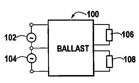
FIG. 1 shows a ballast circuit 100 coupled to first and second AC energy
sources 102,104 and to first and second lamps 106,108. The first energy source
102
provides a first AC input signal and the second AC energy source 104 provides
a
second AC input signal. The first AC input signal enables the ballast to
energize the
first lamp 106 and the second AC input signal enables the ballast to energize
the second
lamp 108. As described below, the ballast 100 independently energizes each of
the first
and second lamps 106,108.
As shown in FIG. 2, the ballast circuit 100 includes a rectifier 110 for
receiving
the first and second AC input signals and for providing DC energy to a boost
converter
112. The boost converter 112 provides DC signal levels to first and second
inverters
114,116 which energize first and second pairs of lamps 106a,b,108a,b,
respectively.
The rectifier 110 also provides a first control signal to the first inverter
114 via a first
control signal path 118, and a second control signal to the second inverter
114 via a
second control signal path 120. The fast control signal 118 is indicative of
whether the
first AC input signal is being applied to the rectifier and the second control
signal 120
is indicative of whether the second AC input signal is present. The first and
second
controls signals are effective to selectively enable the inverters to control
the flow of
energy to the lamps 106,108.
FIG. 3 shows. an exemplary circuit implementation of the ballast circuit 100
of
FIG. 2, wherein like reference designations indicate like elements. The
rectifier 110
includes six rectifying diodes DR1-6 coupled so as to provide first, second,
and third
AC input terminals 122a,b,c and first and second DC output terminals 124a,b.
The
first AC input terminal 122a is located between the first and sixth rectifying
diodes
DR1,DR6, which are coupled end-to-end between the DC output terminals 124a,b.
Similarly, the second AC input terminal 122b is located between the second and
fifth
rectifying diodes DR2,DR5 and the third AC input terminal 122c is located
between the
-5-
CA 02346840 2001-04-10
WO 00/24231 PCTNS99/23402
third and fourth rectifying diodes DR3,DR4. In an exemplary embodiment, the
first
AC input terminal 122a is coupled to a first black wire BLl, the second input
terminal
122b is coupled to white wire W 12, and the third input terminal 122c is
coupled to a
second black wire BL2. The first AC signal can be provided as a conventional
110
volt, 60 Hz signal transmitted via the first black and white wires BL1,W12 and
the
second AC signal can also be provided as a 110 volt, 60 Hz signal transmitted
via the
second black and white wires BL2, W 12. It is understood that the white wire W
12 can
comprise a single wire or a pair of electrically coupled wires, such as, a
first white wire
corresponding to the first black wire BL 1 and a second white wire
corresponding to the
second black wire BL2.
The DC output terminals 124a,b of the rectifier 110 are coupled to the
optional
boost converter 112. The boost converter 112 is effective to boost the voltage
of the
DC signal provided to the inverters 114,116 and to provide power factor
correction.
Boost converters are well known to one of ordinary skill in the art. In one
embodiment
shown in phantom, the boost converter 112 includes a power factor correction
integrated circuit PFC IC coupled to a FET (field effect transistor) QBC for
controlling
a conduction state of the FET. The power factor correction integrated circuit
can be of
the type manufactured by SGS-Thomson Microelectronics of Schaumburg, IL, and
identified as L6560, L6560A, and L6561. The boost converter 112 further
includes a
boost inductor LB and a diode DB which form a series circuit path from the
rectifier
output terminal 124a to the first inverter 1 I4. The boost converter 112'
includes a first
output terminal 126a coupled to a positive rail 128 of the first inverter 114
and a second
output terminal 126b coupled to a negative rail 130 of the first second
inverter.
The first inverter 114 is shown having first and second switching elements
Q1,Q2 coupled in a half bridge arrangement. However, it is understood that
other
inverter configurations are possible, such as full bridge topologies. The
first switching
element Q1, shown as a transistor, has a collector terminal 132 coupled to the
positive
rail 128 of the inverter 114, a base terminal 134 coupled to a first or Q1
control circuit
136, and an emitter terminal 138 coupled to the second switching element Q2.
The
second switching element Q2 has a collector terminal 140 coupled to the
emitter
terminal 138 of the first switching element Q1, a base terminal 142 coupled to
a second
or Q2 control circuit 144, and an emitter terminal 146 coupled to the negative
rail 130
-6-
CA 02346840 2001-04-10
WO 00/24231 PC'f/US99/23402
of the inverter 114. The conduction state of the first switching element Q1 is
controlled
by the first control circuit 136 and the conduction state of the second
switching element
Q2 is controlled by the second control circuit 144.
The first inverter 114 further includes a first resonant inductive element LRl
coupled at one end to a point between the switching elements Q1,Q2 and at the
other
end to a first parallel capacitor CPl. The lamps in the first pair of lamps
106 (first
lamp 106a, second lamp 106b) are coupled end-to-end such that the lamps are
connected in parallel with the first parallel capacitor CPl. First and second
bridge
capacitors CB 1,CB2 are coupled end-to-end between the positive and negative
rails
128,130 of the inverter. The junction of the second lamp 106b and the parallel
capacitor CP1 is coupled to a point between the first and second bridge
capacitors
CB1,CB2.
The second inverter 116 has a configuration that mirrors that of the first
inverter
114. Third and fourth switching elements Q3,Q4 are coupled in a half bridge
configuration between the positive and negative rails 148,150 of the second
inverter 116
with conduction states determined by third and fourth control circuits 152,154
respectively. A resonant circuit is formed by a second resonant inductive
element LR2,
a second parallel capacitor CP2 and the second pair of lamps 108 (third lamp
108a,
fourth lamp 108b). Third and fourth bridge capacitors CB3,CB4 are coupled end-
to-
end across the rails 148,150 of the second inverter 116 with a lamp current
path
connected to a point between the bridge capacitors CB3,CB4.
The first control path 118, which provides a signal path for the first control
signal, extends from the first input terminal 122a of the rectifier 110 to the
second
control circuit 144. The second control path 120, which provides a signal path
for the
second control signal, extends from the third input terminal 122c to the
fourth control
circuit 154. The first control signal is indicative of whether the first AC
input signal
(on wires BL1,W12) is being applied to the first and second input terminals
122a,b of
the rectifier. And the second control signal corresponds to whether the second
AC
input signal (on wires BL2,W12) is present on the second and third terminals
122b,c of
the rectifier. The first and second control signals provide independent
control over the
first and second inverters 114,116. That is, the first inverter 114 can
energize the first
CA 02346840 2001-04-10
WO 00/24231 PCT/US99/23402
pair of lamps 106 when the first AC input signal is present. And the second
inverter
116 can energize the second pair of lamps 108 when the second AC signal is
present.
In operation, the first and second inverters 114,116 each operate at or about
a
characteristic resonant frequency which is determined by the impedances of the
various
circuit elements, such as the respective resonant inductive elements, LR1,LR2,
parallel
capacitors CP1,CP2 and lamps 106,108. For the first inverter 114, current
through the
lamps 106 flows in a first direction while the first switching element Q1 is
conductive
and in a second, opposite direction when the second switching element Q2 is
conductive. The current periodically reverses direction as determined by the
resonant
frequency of the circuit. The first and second control circuits 136,144
control the
respective conduction states of the first and second switching elements Q1,Q2
to
facilitate resonant operation of the circuit.
When the first AC input signal is applied to the rectifier 110, the first
control
signal, via the first control path 118, enables the second control circuit 144
to bias the
second switching element to the conductive state. Thus, when the first AC
signal is
present the first inverter 114 is enabled to resonate such that the ballast
energizes the
first pair of lamps 106 with AC energy which causes the lamps to emit light.
When the first AC signal is not present at the rectifier 110, the first
control
signal conveys this information to the second control circuit 144 which
prevents the
second switching element Q2 from transitioning to a conductive state. Thus,
the first
inverter 114 cannot resonate and is thereby disabled when the first AC signal
is not
applied to the rectifier 110. With the first inverter disabled, the first pair
of lamps 106
is not energized.
Similarly, when the second AC input signal is present at the rectifier 110,
the
second control signal, via the second control path 120, enables the fourth
control circuit
154 to bias the fourth switching element Q4 to a conductive state for resonant
operation
of the second inverter 116. And when the second AC input signal is not
present, the
fourth control circuit 154 prevents the turning on of the fourth switching
element Q4
thereby disabling the second inverter 116.
FIG. 4 shows an exemplary embodiment of the second control circuit 144 of
FIG. 3, wherein like reference designations indicate like elements. The second
control
circuit 144 includes fifth and sixth switching elements QS,Q6 that are
effective to
_g_
CA 02346840 2001-04-10
WO 00/24231 PCT/US99/23402
enable the second switching element Q2 to transition to a conductive state
when the first
AC signal is present on the first control path 118. In general, when the fifth
switching
element Q5 is conductive (i.e., the first AC signal is present) the second
switching
element Q2 can transition to a conductive state to achieve resonant operation
of the first
inverter 114. And when the fifth switching element Q5 is not conductive (i.e.,
the first
AC signal is not present), the sixth switching element Q6 transitions to a
conductive
state which prevents the second switching element Q2 from transitioning to a
conductive state, thereby disabling the first inverter 114.
It is understood that a control path indicating the presence of an AC signal
at the
IO rectifier can be coupled to either or both of the first and second control
circuits
136,144. It is further understood that the second control path 120 is coupled
to the
second inverter 116 (FIG. 3) for selectively enabling the third and/or fourth
switching
elements Q3,Q4.
In the exemplary embodiment of FIG. 4, the second control circuit 144 includes
a first capacitor CQ2B coupled at one terminal to the base terminal 142 of the
second
switching element Q2 and at the other terminal to the negative rail 130 of the
first
inverter. A first resistor RQ2B and inductive bias element L1B provide a
series circuit
path from the base terminal 142 to the negative rail 130. The bias element L1B
is
inductively coupled to the first resonant inductive element L1R such that
current flow
through the first resonant inductive element L1R induces a corresponding
voltage in the
bias element L1B which biases the base terminal 142 of the second switching
element
Q2. As known to one of ordinary skill in the art, as current flow through the
first
resonant inductive element L1R periodically reverses direction due to
resonance of the
circuit, the corresponding voltage induced at the bias element L1B is
effective to
alternately bias the second switching element to conductive and non-conductive
states.
The fifth switching element Q5, shown as a transistor, has a collector
terminal
156 coupled to a point between first and second voltage dividing resistors
RDV1,RVD2, a base terminal 158, and an emitter terminal 160. A zener diode DZ,
a
second resistor RQ5B1 and an enable capacitor CE provide a series circuit path
from
the base terminal 158 of the fifth switching element Q5 to the negative rail
130 of the
first inverter 114. A third resistor RQ5B2 is coupled between the base
terminal 158
and the negative rail 130. An enable diode DE has a cathode 162 coupled to the
enable
-9-
CA 02346840 2001-04-10
WO 00/24231 PCT/US99/23402
capacitor CE and an anode 164 coupled to the first control path 118 which
extends to a
point between the first and sixth diodes DR1,DR6, i.e., the first AC input
terminal
122a of the rectifier 110 (FIG.3).
The sixth switching element Q6 has a collector terminal 166 coupled to the
base
terminal 142 of the second switching element Q2, a base terminal 168 coupled
to an RC
network, and an emitter terminal 170 coupled to the negative rail 130 via a
resistor
RQ6B 1. A capacitor CQ6B is coupled between the base terminal 168 and the
negative
rail 130. A first series circuit path extends from the base terminal 168
through the first
and second voltage resistors RVD1,RVD2, and the bias element L1B to the
negative
rail 130. A second series circuit path extends from the base terminal 168
through a
resistor RQ6B2 and the bias element L1B to the negative rail 130. A diac DD1
is
coupled at one terminal to the base terminal 168 and to the bias element L1B
at the
other terminal.
Referring now to FIG. 4 in combination with FIG. 3, when the first AC input
signal, via the first black and white wires BL1,W12, is applied to the first
and second
input terminals 122a,b of the rectifier 110, the first control signal path 118
provides this
AC signal to the second control circuit 144. The AC signal is rectified by the
enable
diode DE and the enable capacitor CE is charged to a predetermined voltage
level.
When the enable capacitor CE is charged to level greater than a voltage
threshold
associated with the zener diode DZ, the base of the fifth switching element QS
is biased
with a positive potential that is effective to transition QS to a conductive
state. And
when QS is conductive, the sixth switching element Q6 is prevented from
transitioning
to a conductive state. The sixth switching element Q6, when it is in the
conductive
state, effectively shorts the second switching element Q2 thereby disabling
the first
inverter 114. The sixth switching element Q6 can become conductive during
operation
of the circuit unless the fifth switching element QS is turned on by the first
AC signal.
The ballast circuit 100 can be coupled to remotely located first and second
wall
switches which independently control the flow of respective first and second
AC signals
to the ballast. The ballast independently enables the flow of energy to
respective first
and second lamps connected to the ballast. The ballast energizes the first
lamp when
the first AC signal is present and energizes the second lamp when the second
AC signal
-10-
CA 02346840 2001-04-10
WO 00/24231 PCT/US99/Z3402
is present. Thus, a single ballast receives first and second AC input signals
each of
which is effective to energize a respective one of the first and second lamps.
In some areas it is required that, for a light fixture housing four lamps, two
of
the lamps can be turned off. To fulfill this requirement, a typical
configuration
includes a first ballast coupled to a first wall switch and a first pair of
lamps and a
second ballast coupled to a second wall switch and a second pair of lamps. The
first
wall switch controls the first pair of lamps and the second wall switch
controls the
second pair of lamps.
In contrast, a ballast 100 in accordance with the present invention can
independently energize two sets of lamps housed in a single light fixture. In
one
embodiment, a first wall switch, which is coupled to the ballast 100, controls
a first
pair of lamps and a second wall switch, which is also coupled to the ballast
100,
controls a second pair of lamps. Thus, a single ballast 100 independently
energizes
first and second pairs of lamps housed in a fow lamp light fixture.
FIG. 5 shows an alternative embodiment of a ballast 200 having a dual inverter
configuration providing independent control over a plurality of lamps. The
first
inverter 202 can have a half bridge configuration formed from first and second
switching elements Q1,Q2, and the second half bridge inverter 204 can include
third
and fourth switching elements Q3,Q4. The first and second inverters 202,204
are
independently controlled by a first AC input signal on first and second AC
input
terminals 206a,b, e.g., first black wire BL1 and a white wire W, and a second
AC
input signal on the second terminal 206b and a third AC input terminal 206c,
e.g., the
white wire W and a second black wire BL2. The first inverter 202 is disabled
by a first
inverter disable circuit 208 when the first AC input signal is not present and
the second
AC input signal is present. Similarly, the second inverter 204 is disabled by
a second
inverter disable circuit 210 when the first AC input signal is present and the
second AC
input signal is not present.
In one embodiment, a first inductor L 1 A 1 is coupled to the first AC input
terminal 206a and a second inductor L1A2, which is inductively coupled to the
first
inductor L1A1, is coupled to the second AC input terminal 206b. A third
inductor
L1A3, which is inductively coupled to the first and second inductors
L1A1,L1A2,
forms a part of the first inverter disable circuit 208. The first inverter
disable circuit
208 can further include a capacitor CD 1 and a first disc DD 1 coupled to the
base
-11-
CA 02346840 2001-04-10
WO 00/24231 PCTNS99/23402
terminal Q5B of a transistor Q5, which has a collector terminal Q5C coupled to
the
base terminal Q2B of the second switching element Q2 of the first inverter
202.
Similarly, a fourth inductor L1B1 is coupled to the second AC input terminal
206b, a fifth inductor L1B2 is coupled to the third AC input terminal 206c,
and a sixth
inductor L1B3, which forms part of a second inverter disable circuit 210, is
coupled to
a sixth switching element Q6 for controlling a switching transistor Q4 of the
second
inverter 204. The second inverter disable circuit can further include a
capacitor CD2
and a second disc DD2 coupled to the transistor Q6 for selectively disabling
the second
inverter.
In operation, the flux generated by,the first and second inductive elements
L1A1,L1A2 cancels each other when the first AC input signal is present on the
first and
second terminals. In the case where the second AC input signal is present, and
the first
AC input signal is not present, the flux generated by the second inductor L1A2
is not
canceled such that a voltage is generated on the third inductor L1A3, which
charges the
capacitor CD1. When the voltage on the capacitor CDI rises above a
predetermined
threshold, the first disc DDl triggers and the fifth switching element Q5
transitions to
the conductive state. This effectively prevents the second switching element
Q2 of the
first inverter from transitioning to the conductive state, thereby disabling
the first
inverter 202.
Similarly, when the first AC input signal is present and the second AC input
signal is not present, a voltage is generated on inductive element L1B3 to
disable the
second inverter 210.
FIG. 6 shows an exemplary circuit implementation of the circuit 200 of FIG. 5
adapted for 120 V operation. FIG. 7 shows a similar circuit implementation
adapted
for 277 Volt operation. Various other features of these circuits are shown and
described, for example, in co-pending and commonly owned U.S. Application Nos.
09/173,850, 09/173,852, and 09/173,966, all filed on October 16, 1998, and all
incorporated herein by reference.
FIG. 8 shows a ballast 300 in accordance with the present invention that
independently energizes first and second lamps L1,L2 with a common inverter
302
energized by a rectifier 304. In an exemplary embodiment, the ballast 300
includes a
first input terminal 306a far coupling to a first black wire B1 and a second
input
terminal 306b for coupling to white wire W. A third input terminal 306c and
the
-12-
CA 02346840 2001-04-10
WO 00/24231 PCTNS99/23402
second input terminal 306b are adapted for coupling to a second black wire B2
and the
white wire W, respectively. A first AC input signal corresponds to the first
black wire
B1 and the white wire W and a second AC input signal corresponds to the second
black
wire B2 and the white wire W.
A first signal detector 308 is coupled to the first input terminal 306a and to
a
first lamp control circuit 310 via a first control signal path 312. The first
signal
detector 308 provides a first control signal to the first lamp control circuit
310 that is
indicative of whether the first AC input signal is present. A second signal
detector 314
is coupled to the third input terminal 306c and to a second lamp control
circuit 316 via
a second control signal path 318. The second signal detector 314 provides a
second
control signal to the second lamp control circuit 316 that is indicative of
whether the
second AC input signal is present. The first and second signal detectors
308,314 are
coupled together at a node 320 that is also connected to the rectifier 304.
The second
input terminal 306b is also connected to the rectifier 304.
The first lamp L1, a first capacitor C1 and the first lamp control circuit 310
form a first series circuit path and the second lamp L2, a second capacitor C2
and the
second lamp control circuit 316 form a second series circuit path. The first
and second
series circuit paths are coupled across first and second terminals 320a,b of
the inverter,
which provide a drive signal to the first and second lamps L1,L2.
In one embodiment, the first lamp L1 is coupled between the first capacitor
C1,
which is coupled to the first inverter terminal 320a, and the first lamp
control circuit
310, which is coupled to the second inverter terminal 320b. Similarly, the
second lamp
L2 can be coupled between a second capacitor C2 and the second lamp control
circuit
316.
In operation, the rectifier 304 energizes the inverter 302 when either of the
first
and second AC input signals is present. When the first AC input signal is
present on
the first and second terminals 306a, b, the first signal detector 308 sends a
"signal
present" indication to the first lamp control circuit 310 via the first signal
path 312.
The first lamp control circuit 310 then enables the flow of current through
the first lamp
L1. Similarly, when the second AC signal is present on the second and third
terminals
306b, c, the second signal detector 314 sends a "signal present" indication to
the second
lamp control circuit 316, which then enables the second lamp L2 to be
energized.
-13-
CA 02346840 2001-04-10
WO 00/24231 PCTIUS99/23402
In the case where the first and second AC input signals are both present, the
first and second capacitors C1,C2 buffer the high frequency signal from the
inverter
302 such that the first lamp to light does not prevent the other lamp from
lighting due to
excessive current draw by the first lighted lamp.
FIG. 9 shows an exemplary circuit implementation of the ballast 300 of FIG. 8.
The first signal detector 308 includes a first optocoupler 350 having a first
terminal 352
coupled to the first input terminal 306a and a second terminal 354 coupled to
the first
terminal 356 of a second optocoupler 358, which corresponds to the second
signal
detector 314. In one embodiment, the first optocoupler 350 includes first and
second
light emitting diodes DOCA,DOCB coupled in parallel and in opposite polarity.
The
second optocoupler 358 can include first and second diodes DOCC,DOCD connected
in
a similar manner.
The rectifier 304 includes diodes DRl-4 coupled in a full bridge configuration
as shown. The node 360 formed by the second terminal 354 of the first
optocoupler
350 and the first terminal 356 of the second optocoupler 358 is coupled to a
point 360
between the first and third rectifier diodes DRI,DR3. The second AC input
terminal
306b is coupled to a point between the second and fourth rectifier diodes
DR2,DR4.
In one embodiment, the first lamp control circuit 310 includes a first
optically
coupled transistor QOC1 forming a part of the first optocoupler 350. The
transistor
QOC1 can include a collector terminal 362 coupled to the first lamp Ll, a base
terminal
364 optically coupled via signal path 312 to the first optocoupler diodes
DOCA,DOCB,
and an emitter terminal 366 coupled to the second terminal 320b of the
inverter via a
resistor Rl. The first lamp control circuit 310 can further include a first
control
transistor Q1 having a collector terminal 370 connected to the collector
terminal 362 of
the first optically coupled transistor QOC1, a base terminal 372 coupled to
the emitter
366 of transistor QOC1, and an emitter terminal 374 coupled to the second
inverter
terminal 320b. A first diode D1 includes an anode 376 coupled to the second
terminal
320b and a cathode 378 coupled to the first lamp Ll and to the collector
terminals of
the transistors Q1,QOC1.
The second lamp control circuit 316 can also include a transistor QOC2
optically coupled to the second optocoupler 358 via signal path 318, a control
transistor
Q2, and a diode D2, coupled in manner similar to the first lamp control
circuit 310.
-14-
CA 02346840 2001-04-10
WO 00/24231 PCT/US99/23402
When the first AC signal is present, the light emitting diodes (LEDS)
DOCA,DOCB will bias the first optically coupled transistor QOC1 to a
conductive
state, which transitions the first control transistor Q 1 to the conductive
state. The
conductive control transistor Q1 provides a path for current to flow from the
first
terminal 320a of the inverter to the second terminal 320b and the diode D 1
provides a
path for current to flow from the second terminal 320b to the first terminal
320a. Thus,
the AC signal from the inverter 302 can energize the first lamp L1.
When the first AC signal is not present, the diodes DOCA,DOCB in the first
optocoupler 350 are not activated and the first optically coupled transistor
QOC1 does
not bias the control transistor Q1 to a conductive state. Thus, there is no
path for
current to flow from the first inverter terminal 320a, thereby disabling the
first lamp
L1.
Similarly, when the second AC signal is present, the light emitting diodes
DOCC,DOCD in the second optocoupler 358 are activated, which biases the second
optically coupled transistor QOC2 to a conductive state. This transitions the
second
control transistor Q2 to the conductive state such that the transistor Q2 and
the second
diode D2 allow current flow between the first and second inverter terminals
320a,b to
energize the second lamp L2.
Thus, the first AC input signal energizes the first lamp Ll independently of
whether the second AC input signal is present and the second AC input signal
energizes
the second lamp L2 independently of whether the first AC signal is present.
The ballast
provides independent lamp control with a relatively high degree of circuit
component
commonality.
It is understood that the number of lamps can vary without departing from the
invention. For example, first and second lamps coupled in series can be
energized
independently from third and fourth lamps coupled in series across first and
second
terminals of an inverter. It is further understood that the signal paths used
to couple the
signal detection circuits the lamp control circuits can includes conductive
pathways,
optical couplings, inductive couplings, and other such connections known to
one of
ordinary skill in the art. In addition, one of ordinary skill in the art will
readily
appreciate that other types of switching elements can be substituted for those
shown and
described herein and that the particular circuit arrangements can be modified.
-15-
CA 02346840 2001-04-10
WO 00/24231 PGTNS99lZ3402
One skilled in the art will appreciate further features and advantages of the
invention based on the above-described embodiments. Accordingly, the invention
is not
to be limited by what has been particularly shown and described, except as
indicated by
the appended claims. All publications and references cited herein are
expressly
incorporated herein by reference in their entirety.
What is claimed is:
-16-