Note: Descriptions are shown in the official language in which they were submitted.
CA 02347604 2001-05-15
IaERG2515/C2448 PATENT
ELECTRICAL CONNECTOR CAPABLE OF EXERTING A SELECTIVELY
VARIABLE CONTACT FORCE
',Field of the Invention
The present invention relates generally to electrical connectors. More
particularly, the
:invention relates to an electrical connector that is capable of exerting a
contact force that can
'be selectively varied.
Background of the Invention
Electrical connectors typically incorporate one or more conductive contacts.
The
contacts are typically mated to the contacts of another connector to establish
an electrical path
between the connectors. For example, a common receptacle-type connector may
incorporate
one or more contact beams that slidably engage a male contact of a mating
connector, thereby
forming a conductive path between the connectors.
Mating first and second electrical contact gives rise a contact force between
the
respective contacts. Establishing an appropriate contact force between the
contact pair is
critical to the proper operation of the connectors. For example, the contact
force must be
CA 02347604 2001-05-15
13ERG2515/C2448 -2- PATENT
large enough to ensure that the contacts tightly engage. Insufficient
engagement can result in
poor electrical conductivity (and high signal losses). Excessive contact
force, however, can
lead to several problems. For example, high contact forces can make it
difficult to mate the
connectors, and can damage the contacas. High contact forces can also inhibit
the removal of
S the male contact from the mating connector. This problem is particularly
troublesome in
unmating connectors that incorporate large numbers of contacts, as the contact
forces
~~ssociated with each individual contact can combine to generate excessive
insertion and
removal forces.
Furthermore, high contact forces can produce excessive wiping action during
insertion
and removal of the male contact. Excc;ssive wiping action can result in
premature wear of the
contacts. Excessive wiping action can also erode the various coatings that are
commonly
applied to contacts, e.g., gold plating.
Hence, the contact force generated by a given connector pair must be
considered when
deciding whether the connector pair is appropriate for a particular
application. For example,
certain applications may require very llow signal losses. A connector pair
that generates a
relatively large contact force may be appropriate for such applications,
particularly where
lFrequent insertion and removal of the male contact is not anticipated.
Conversely, a
connector pair that generates a relatively low contact force may be
appropriate where frequent
iinsertion and removal of the male contact will occur, and where minimal
signal losses are not
~~n absolute necessity.
Conventional connectors produce a fixed, i.e., non-variable, contact force.
Hence,
.different types of connectors must be utilized in applications that require
different contact
forces. A connector manufacturer must therefore produce a different type of
connector for
each application that requires a differc;nt contact force. This is true even
where all of the
other requirements for the connector acre identical, e.g., overall size,
number and type of
individual contacts, etc.
The above discussion illustrates the current need for a connector that is
capable of
exerting a contact force that can be varied among different values. Such a
connector could be
used in a variety of different applications that each require different
amounts of contact force,
thereby eliminating the need to produce different types of connectors for each
of the various
applications.
CA 02347604 2001-05-15
IBERG2515/C2448 -3- PATENT
Utilizing a single connector configuration in a variety of different
applications can
lead to potentially significant cost savings. For example, manufacturing costs
can be lowered
by reducing the number of different hardware configurations that need to be
produced for a
given number of applications. Savings in inventory, packaging, and marketing-
related
c;xpenses can also be realized by using; a single type of connector in place
of multiple
connector types. Also, the use of a connector that is capable of exerting a
variable contact
iEorce can allow the contact force to be more closely tailored to an optimal
value than may
otherwise be possible.
;Summary of the Invention
An object of the present invention is to provide an electrical connector that
is capable
~of exerting a contact force that can be selectively varied. In accordance
with this object, a
;presently-preferred embodiment of the invention provides an electrical
connector for mating
with a male contact of a mating connector. The connector module comprises a
conducting
member including a lead and a contact beam electrically coupled to the lead.
The contact
beam is adapted to resiliently engage the male contact. The connector module
further
comprises a contact housing. At least: a portion of the lead is disposed
within the contact
housing. At least a portion of the contact beam is disposed within the contact
housing so that
the contact beam is urged into and restxained by the contact housing when the
contact beam
resiliently engages the male contact. A contact force is thereby generated
between the contact
beam and the contact pin.
The contact housing in one particular preferred embodiment is capable of being
selectively positioned in relation to tree contact beam so that a point of
restraint on the contact
beam is selectively variable. The contact force between the contact beam and
the male
contact can thereby be varied on a selective basis.
Further in accordance with the above-noted object, another presently-preferred
embodiment of the invention provides an electrical connector for mating with a
male contact
of a mating connector. The electrical) connector comprises a conducting
element having a
lead. The conducting element also includes a contact beam having a first end
that is fixedly
coupled to the lead. The contact beam also has a second free-standing end for
resiliently
CA 02347604 2001-05-15
q HERG-2515/C2448 -4- PATENT
engaging the male contact so that the contact beam deflects when the contact
beam engages
tike male contact.
The electrical connector further comprises a housing that is adapted to
inhibit the
dleflection of the contact beam by restraining the contact beam at a point of
restraint located
between the first and the second ends of the contact beam, whereby a contact
force is
generated between the contact beam and the male contact and the contact force
is dependent
upon the location of the point of restraint on the contact beam.
A further object of the present :invention is to provide a method of adjusting
a spring
rate of a contact in an electrical connector. In accordance with this object,
a presently-
yreferred method of adjusting a spring rate of a contact in an electrical
connector before the
connector engages a mating connector comprises the step of providing an
electrical connector
with a housing and a deflectable contact, the housing being positionable
relative to the
contact at a plurality of positions. The: preferred method further comprises
the step of
positioning the housing at a predetermined one of the plurality of positions,
wherein the
predetermined position of the housing determines the spring rate of the
contact.
A further object of the present invention is to provide a kit for making an
electrical
connector. In accordance with this object, a presently-preferred embodiment of
the invention
provides a kit for making an electrical connector having a contact with a
predetermined
spring rate. The kit comprises a plurality of housings and a deflectable
contact mountable to
~~ny one of the plurality of housings to form an electrical connector, wherein
the housings can
engage the contact to provide a predetermined spring rate to the contact, and
each one of the
:housings provides a different predetermined spring rate.
Brief Description of the Drawings
The foregoing summary, as well as the following detailed description of a
presently-
preferred embodiment, is better understood when read in conjunction with the
appended
drawings. For the purpose of illustrating the invention, the drawings show an
embodiment
that is presently preferred. The invention is not limited, however, to the
specific
instrumentalities disclosed in the drawings. In the drawings:
_ _..... _
Fig. 1 is a side view of an electrical connector in accordance with the
present
invention;
CA 02347604 2001-05-15
~tERG2515/C2448 -5- PATENT
Fig. 2 is an exploded perspective view of a connector module of the electrical
connector shown in Fig.l;
Fig. 3 is another exploded perspective view of the connector module shown in
Fig. 2;
Fig. 4 is a top perspective view of a contact portion of the connector module
shown in Figs. 2 and 3;
Fig. 5 is a top perspective view of a forward portion of a contact housing of
the connector module shown in Figs. 2 and 3;
Fig. 6A is a forward-side view of the contact housing shown in Fig. 5 located
in a rearward position on the electrical connector shown in Fig. 1;
Fig. 6B is a forward-side view of the contact housing shown in Figs. 5 and 6A
v~rith the contact housing located in an intermediate position on the
electrical connector shown
in Fig. l;
Fig. 6C is a forward-side view of the contact housing shown in Figs. 5, 6A,
1 S and 6B with the contact housing located in a forward position on the
electrical connector
shown in Fig. 1;
Fig. 7A is a side view of the contact portion shown in Fig. 4 and a cam
surface
of the contact housing shown in Figs. _'> and 6A-6C, with the contact housing
positioned as
depicted in Fig. 6A;
Fig. 7F is a side view of the contact portion shown in Figs. 4 and 7A and a
cam surface of the contact housing shown in Figs. 5 and 6A-6C, with the
contact housing
positioned as depicted in Fig. 6B;
Fig. 7C is a side view of the contact portion shown in Figs. 4, 7A, and 7B and
a~ cam surface of the contact housing shown in Figs. 5 and 6A-6C, with the
contact housing
~ positioned as depicted in Fig. 6C;
Fig. 8 is a side view of the contact portion shown in Figs. 5 and 7A- 7C
engaging a male contact;
Fig. 9 is a top perspective view of an alternative embodiment of the
electrical
connector shown in Figure 1;
_ _ _-.- - _
Fig. l0A is rear perspective view of an outer contact housing of another
alternative embodiment of the electrical connector shown in Figure 1;
CA 02347604 2001-05-15
)BtERG2515/C2448 -6- PATENT
Fig. l OB is a side view of the outer contact housing shown in Fig. 10A;
Fig. 11 A is a side view of the outer contact housing shown in Figs. l0A and
l OB about to engage a contact housing.;
Fig. 11B is a side view of the outer contact housing shown in Figs. 10A, 10B,
and 11 A partially engaging the contact housing shown Fig. 11 A; and
Fig. 11 C is a side view of the outer contact housing shown in Figs. 10A, l
OB,
11 A, and 11 B fully engaging the contact housing shown in Figs. 11 A and 11
B.
Tlescription of Preferred Embodiments
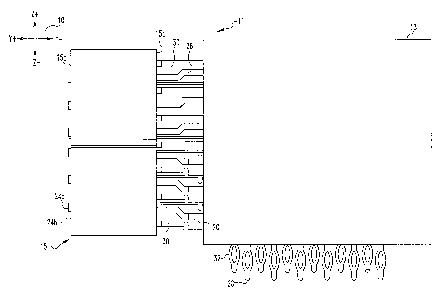
A presently-preferred embodiment of the invention is illustrated in Figures 1
through
8. The figures are each referenced to a. common coordinate system 10 shown in
each
illustration. The invention provides an electrical connector 11 formed by a
plurality of
connector modules 12. The electrical connector 11 is adapted to mate with one
or more male
contacts of a mating connector. The electrical connector 11 also comprises an
electrically
insulative main housing 13. The connector modules 12 are at least partially
disposed within
the main housing 13, as explained in detail below.
Each of the connector modules 12 comprises a contact housing 15, an overmold
18, a
1>lurality of conducting members 20, and a ground assembly 22 (see Figures 2
and 3). The
conducting member 20 is formed fromi an electrically-conductive material. The
conducting
member 20 comprises a contact portion 24 (see Figure 4). The contact portion
24 includes a
ride contact beam 24a, a lower contact beam 24b, and a rearward portion 24c.
Preferably, the
contact beam 24a, the lower contact beam 24b, and the rearward portion 24c are
unitarily
formed. The rearward portion 24c ha;. a substantially L-shaped cross section.
The contact
beams 24a and 24b extend from the rearward portion 24c, and are disposed in
substantially
parallel orientations.
The side contact beam 24a includes a contact tab 24d (see Figure 4). The lower
.contact beam 24b likewise includes a contact tab 24e. The contact tabs 24d
and 24e form the
forward ends of the respective contact: beams 24a and 24b. (The "forward" and
"rearward"
directions correspond respectively to the y+ and y directions denoted on the
coordinate
.,.._. -
system 10.) A cam surface 24f is formed on an upper edge 24g of the rearward
portion 24c.
CA 02347604 2001-05-15
BERG-2515/C2448 -7- PATENT
E~ cam surface 24h is likewise formed on a side edge 24i of the rearward
portion 24c. The
significance of the cam surfaces 24h and 24j is discussed below.
The contact member 20 further comprises a signal lead 26 and a contact pin 28
(see
Figures 2 and 3). A first end of the signal lead 26 is mechanically coupled to
the contact pin
2;8. An opposing second end of the signal lead 26 is mechanically coupled to
the rearward
portion 24c of the contact portion 24. This arrangement forms an electrical
path between the
contact pin 28 and the contact portion 24. Each signal lead 26 includes one or
more bends
that cause the contact portions 24 and the contact pins 28 to extend in
substantially
perpendicular directions.
The ground assembly 22 is fonned from an electrically-conductive material. The
l;round assembly 22 includes a plurality of ground leads 30 (see Figures 2 and
3). Each
l;round lead 30 adjoins one or more adjacent ground leads 30. A first end of
each ground lead
:30 is mechanically coupled to a contact pin 32. An opposing second end of
each ground lead
:30 is mechanically coupled to a first ground contact 34a and a second ground
contact 34b.
'Chis arrangement electrically couples the contact pin 32 and the ground
contacts 34a and 34b.
Mach ground leads 30 includes one or more bends that cause the ground contacts
34a and 34b
lie substantially perpendicular to the contact pins 32.
The overmold 18 is formed from an electrically insulative material such as
plastic.
'The overmold 18 has a forward face 18a and a lower face 18b (see Figures 2
and 3). 'The
:forward face 18a and the lower face 18b are disposed in substantially
perpendicular
orientations. The overmold 18 is molded around the signal leads 26 of the
contact member
:20. More particularly, the overmold 18 partially encloses the signal leads 26
so that a portion
~of each signal lead 26 and the corresponding contact portion 24 extend away
from the
forward face 18a and the contact pins 28 extend away from the lower face 18b.
The overmold 18 includes a plurality of grooves 18c (see Figure 3). The
grooves 18c
extend between the forward face 18a .and the lower face 18b. Each ground lead
30 of the
ground assembly 22 is partially disposed within a corresponding groove 18c. A
portion of
each ground lead 30 and the corresponding ground contacts 34a and 34b extend
away from
the forward face 18a of the overmold 18 when the ground leads 30 are partially
disposed
_.,.". _
within the grooves 18c. In addition, the contact pins 32 of the ground
assembly 22 extend
away from the lower face 18b of the overmold 18 when the ground leads 30 are
so disposed.
CA 02347604 2001-05-15
~tERG2515/C2448 -8- PATENT
Each overmold 18 can accommodate six conducting members 20 and six ground
assemblies 22. Alternative embodiments of the overmolds 18 may accommodate any
desired
number of conducting members 20 andl ground assemblies 22. The contact
portions 24 of the
conducting members 20 in each connector module 12 are substantially vertically
aligned (see
Figures 2, 3 and 6A-6C). The contacts 34a and 34b of the ground assemblies 22
in each
connector module 12 are likewise substantially vertically aligned. The
connector module 12
is shown in a single-ended arrangement. Alterative embodiments of the
connector module 12
nnay comprise two columns of ground contacts 34a, 34b and two columns of
contact portions
2;4 for a differential-pair arrangement.
The exemplary electrical connector 11 includes thirteen of the connector
modules 12
disposed in a side-by-side arrangement. In other words, the connector modules
12 are
positioned so that the forward faces 18a of the overmolds 18 are substantially
co-planar, and
the lower faces 18a of the overmolds 18 are also substantially co-planar. The
modules 12 are
then inserted into the larger main housing 13 to fonm the electrical connector
11. The main
housing 13 of the exemplary embodirr~ent encloses a portion of the connector
modules 12. In
particular, the main housing 13 does not enclose the portions of the connector
modules 12
l:orward of the ovenmolds 18 (see Figure 1 ). The remaining portions of the
connector
modules 12 are substantially enclosed by the main housing 13. Alternative
embodiments of
the main housing 13 may be sized so that the main housing 13 encloses a
substantial entirety
of the connector modules 12. Further variants of the main housing 13 are
discussed in detail
'below.
Structural details relating to the contact housing 15 are as follows. Figures
1, 3 and
6A-6C show the contact housing 1 S installed on the connector module 12. The
contact
housing 15 is also depicted in Figure 2.
A plurality of passages 38 are formed within the contact housing 15 (see
Figures 2, 3,
and 6A-6C). Figure 5 is a detailed diagrammatical illustration showing one of
the passages
38. Each passage 38 is defined by a top wall 38a, an opposing bottom wall 38b,
a first side
wall 38c, and a second side wall 38d that opposes the first side wall 38c. A
cam surface 38e
is fonmed on the bottom wall 38b (see Figure 5). The significance of this
feature is discussed
in detail below. Each passage 38 extends between (and through) a forward edge
15a and a
rearward edge 1 Sb of the contact housing 15. The passages 38 are arranged so
that the
CA 02347604 2001-05-15
13ERG-2515/C2448 -9- PATENT
vertical spacing between the individual passages 38 substantially matches the
vertical spacing
t>etween the contact portions 24 of the contact members 20. The function of
the passages 38
is explained below.
The contact housing 15 defines a plurality of troughs 39 (see Figures 2, 3,
and 6A-
fiC). The troughs 39 are positioned between the passages 38. Each trough 39
extends
between (and through) the forward anti rearward edges 15a and 15b of the
contact housing
l~ 5. The function of the troughs 39 is discussed in detail below.
The contact housing 15 engages the contact portions 24 of the conducting
member 20.
l:n accordance with the present invention, the contact housing 15 can be
variably positioned in
relation to the contact beams 24a and 24b. This feature permits the contact
force between
each lower contact beam 24b and a corresponding male contact of a mating
connector to be
;selectively varied, as explained in det<~il below.
The contact housing 15 is engaged with the contact portions 24 by aligning
each of
the passages 38 with one of the contact portions 24 of the conducting members
20. An
insertion force is subsequently applied to the contact housing in the rearward
(y) direction.
The insertion force causes the contact portions 24 to become disposed within
the passages 38.
In addition, the ground contacts 34a and 34b become disposed within the
troughs 39.
The passages 38 are sized so that the cam surface 24f of each side contact
beam 24a
slidably engages the top wall 38a of a. respective passage 38 as the contact
housing 15 is
mated to the contact portions 24. In addition, the cam surface 24h of each
lower contact
beam 24b slidably engages the side wall 38c of a respective passage 38 as the
contact housing
15 is mated to the contact portions 24. Frictional forces between the cam
surfaces 24g and
24h and the respective passage walls 38a and 38c cause the contact housing 15
to remain in
position once the insertion force is removed. Alternatively, the passages 38
may be equipped
with detents that engage the cam surfaces and thereby lock the contact housing
into one of a
limited number of possible positions.
The cam surface 38e on the bottom wall 38b of each passage 38 slidably engages
a
corresponding lower contact beam 24b as the contact housing 1 S is mated to
the contact
portions 24. More particularly, each cam surface 38e slidably engages a lower
surface 24j of
.,_. -
the corresponding lower contact beam 24b (see Figures 7A-7C and 8).
CA 02347604 2001-05-15
>EtERG-2515/C2448 -10. PATENT
The cam surface 38e contacts the lower surface 24j at a point of contact 43.
The point
o~f contact 43 is dependent upon the relative positions of the contact housing
15 and the
contact portions 24. For example, the contact housing 15 can be placed in a
forward position
as shown in Figure 6C. Positioning the contact housing 15 in this manner
causes the point of
contact 43 to be located at its forward-most position along the lower contact
beam 24b, as
shown in Figure 7C. In other words, the point of contact 43 is located in
relatively close
proximity to the contact tab 24e of the lower contact beam 24 when the contact
housing 1 S is
placed in its forward position.
The contact housing 15 can also be placed in an intermediate position as shown
in
Figure 6B. Moving the contact housing 15 from its forward position to an
intermediate
position increases the distance between the point of contact 43 and the
contact tab 24e, as
shown in Figure 7B. The contact housing 15 can also be placed in a rearward
position (see
Figure 6A). Positioning the contact housing 15 in this manner causes the point
of contact 43
t~ be located at its rearward-most position along the lower contact beam 24b,
as shown in
Figure 7A. In other words, the point of contact 43 is located at its farthest
position from the
contact tab 24e when the contact housing 1 S is placed in its rearward
position. The
significance of variably positioning the point of contact 43 in this manner is
explained in
detail below.
The contact portions 24 of the contact members 20 are adapted to engage a male
contact of a mating connector, as noted previously. Figure 8 depicts one of
the contact
portions 24 mated to a male contact 40 of a mating connector. The contact
portion 24 and the
male contact 40 are mated by sliding the male contact 40 rearward, in the
direction denoted
by the arrow 46 in Figure 8. The rearward movement of the male contact 40
causes the
contact tab 24e (and the adjacent portion of the lower contact beam 24b) to
deflect
downward, in the direction denoted by the arrow 48.
The deflection of the lower contact beam 24b is restrained by the cam surface
38e on
l:he bottom wall 38b of the passage 38. The restraining effect of the cam
surface 38e, in
conjunction with the resilience of the lower contact beam 24b, causes a
contact force to
develop between the male contact 40 and the lower contact beam 24b (this force
is commonly
referred to as the "spring rate" of the contact 40). A contact force also
develops between the
:male contact 40 and the side contact beam 24a. A detailed discussion of this
contact force is
CA 02347604 2001-05-15
13ERG-2515/C2448 -11- PATENT
not necessary to an understanding of the invention. Hence, the contact force
between the side
contact beam 24a and the male contact 40 will not be discussed in detail.
The contact force between the lower contact beam 24b and the male contact 40
is
dependent upon the location of the point of contact 43 between the lower
contact beam 24b
and the cam surface 38. More particularly, the downward deflection of the
lower contact
beam 24b, in conjunction with the restraining effect of the cam surface 38e,
causes the
contact tab 24e to pivot about the cam surface 38e (and the point of contact
43). The
resistance of the contact beam 24b to such rotation is inversely proportional
to the moment
arm between the location of the applied force (the contact tab 24e) and the
point of rotation
I',the point of contact 43). Hence, the resistance of the contact beam 24b
(and the resulting
contact force between the male contact 40 and the lower contact beam 24b) can
be varied by
;altering the distance between the contact tab 24e and the point of contact
43. In other words,
'the effective beam length of the lower contact beam 24b can be altered by
varying the
location of the point of contact 43.
The distance between the contact tab 24e and the point of contact 43 can be
varied
through the selective placement of the; contact housing 1 S, as explained
above. For example,
placing the contact housing 15 in its fbrward position minimizes the distance
between the
contact tab 24e and the point of contact 43 (see Figures 6C and 7C). Thus, the
length of the
moment arm between the contact tab 24e and the point of contact 43 is at a
minimum when
the contact housing 15 is so positioned. The relatively small moment arm
causes the lower
contact beam 24b to exert a relatively large amount of resistance when the
contact tab 24e is
deflected downward by the male contact 40. Hence, the contact force between
the lower
contact beam 24b and the male contact 40 is relatively high when the contact
housing 15 is
located in its forward position.
Conversely, placing the contact housing 15 in its rearward position maximizes
the
distance between the contact tab 24e and the point of contact 43, and thereby
maximizes the
length of the moment arm between the contact tab 24e and the point of contact
43 (see
Figures 6A and 7A). The relatively large moment arm causes the contact tab 24e
to rotate
about the point of contact 43 with a relatively low amount of resistance_when
the contact tab
24e is deflected downward by the male contact 40. 'Thus, the contact force
between the
contact beams 24 and the male contact 40 is relatively low when the contact
housing 15 is
CA 02347604 2001-05-15
BERG-2515/C2448 -12- PATENT
positioned in this manner. Placing the contact housing 15 in an intermediate
position causes
the length of the moment arm to lie between its maximum and minimum values.
Hence, the
contact force lies between its maximum and minimum values when the contact
housing 15 is
located in an intermediate position. The contact housing 15 remains at a fixed
position
relative to the contact 24 once the connector is assembled, thereby producing
a uniform
spring rate. In other words, the spring rate does not vary after the connector
is assembled.
The invention thus permits the contact force between an array of male contacts
such
~~s the contacts 40 and an electrical cormector such as the electrical
connector 11 to be varied
within a range of values using a common hardware configuration. This feature
permits a
:jingle type of electrical connector to be used in various applications that
each require a
different amount of contact force. Utilizing a common electrical connector in
a variety of
different applications offers substantial benefits. For example, the use of a
common electrical
connector reduces the number of different components that the connector
manufacturer must
produce. Such reductions can lead to substantially lower production costs.
1 S In addition, inventory-related c;xpenses to both the manufacturer and the
user of the
common electrical connector can be lowered by reducing the number of different
types of
connector modules that need to be tracked and stored prior to use. Also, the
costs associated
with packaging and marketing a multitude of different connector types can be
lowered by the
use of the common electrical connector.
Furthermore, the ability to vary the contact force of the electrical connector
can allow
the contact force to be more closely tailored to a desired value than may
otherwise be
feasible. More particularly, an electrical connector that produces a desired
amount of contact
force may be unavailable for a particular application, thereby necessitating
the use of an
electrical connector that produces a less-than-optimal amount of contact
force. The use of an
electrical connector such as the connector 11 permits the contact force to be
set within a range
of values, as noted above. This feature provides the user of the electrical
connector with
greater flexibility in choosing the actual contact force, and thereby
increases the potential for
the contact force to be set at or near ita optimal value.
It is to be understood that even though numerous characteristics and
advantages of the
present invention have been set forth in the foregoing description, together
with details of the
structure and function of the invention, the disclosure is illustrative only,
and changes may be
CA 02347604 2001-05-15
IBERG2515/C2448 -13- PATENT
made in detail, especially in matters of shape, size, and arrangement of the
parts, within the
principles of the invention to the full extent indicated by the broad general
meaning of the
terms in which the appended claims aJ-e expressed.
For example, the contact force between the side contact beam 24a and the
.corresponding male contact 40 is not variable in the exemplary electrical
connector 11.
Alternative embodiments of the invention may incorporate features that permit
the contact
force between the side contact beam 2;4a and the male contact 40 to be varied.
Another possible variant of the invention forgoes the use of the contact
housings 1 S.
The contact force between the contact: beams 24a and 24b and the respective
male contacts 40
of this embodiment is determined by 'the overall length (x dimension) of each
overmold 18.
More particularly, each overmold 18 is formed in a manner that causes the
contact beams 24a
and 24b to extend through the forward face 18a, i.e., the forward face 18a is
formed around
the rearward portions of the contact beams 24a and 24b. The forward face 18a
thereby
restrains the contact beams 24a and 24b when the contact beams 24a and 24b are
deflected by
the respective male contacts 40. The length of the overmold 18 determines the
location of the
forward face 18a in relation to the contact beams 24a and 24b. Hence, the
length of the
overmold 18 determines the points of restraint of the contact beams 24a and
24b and, thus,
the respective contact forces between. the contact beams 24a and 24b and the
male contacts
40.
Figure 9 shows another possible variant of the present invention. Figure 9
depicts an
electrical connector l la having a main housing 13a a fixed outer contact
housing 49. The
electrical connector 11 a is otherwise substantially identical to the
electrical connector 11.
Structure on the electrical connector 11 a that is substantially identical to
corresponding
structure on the electrical connector 11 is described herein using like
reference numerals.
The fixed outer contact housing 49 is positioned over the contact housings 1 S
and the
contact portions 24 of the conducting members 20 after the contact housings 1
S have been
placed in their desired positions relative to the contact portions 24. The
outer contact housing
49 is fixed to the main housing 13a by way of an interlocking latch 13b on the
main housing
13a _that engages a projection 49a on the outer contact housing 49.
Penetrations 49b are
formed in a forward edge 49c of the fixed outer contact housing 49 to
facilitate access to the
contact portions 24 by the male conl:acts 40.
CA 02347604 2001-05-15
1BERG-2515/C2448 -14- PATENT
A further alternative embodiment is shown in Figures l0A through 11C. Figures
l0A
~;hrough 11C depict a portion of an electrical connector l lb having a movable
outer contact
housing 50 and contact housings 15c. Each contact housing 1 Sc includes a fin
15d located
along an upper surface of the contact lousing 15c (see Figures 11A-11C). The
electrical
connector l lc is otherwise substantially identical to the electrical
connector 11. Structure on
l:he electrical connector 11 c that is substantially identical to
corresponding structure on the
electrical connector 11 is described herein using like reference numerals.
The movable outer contact housing SO is adapted to enclose the contact
housings 1 Sc.
'The outer contact housing 50 is selectively positionable along with the
contact housings 15c.
'The outer contact housing SO is placed over the contact housings 15c by
sliding the outer
contact housing 50 in a rearward direction over the contact housings 15c (the
rearward
direction is denoted by an arrow 52 shown in Figures 1 lA and 11B). Grooves
SOa defined by
.an upper inner surface SOb of the outer contact housing 50 slidably engage
the fins 15d on the
.contact housings 15c as the housing 50 is slid rearward.
The rearward movement of the outer contact housing SO eventually causes a
forward
.edge 15e of each fin 15d to abut a forward edge SOc of the corresponding
groove SOa (see
Figure 11 C). Continued rearward movement of the housing 50 causes the outer
contact
housing SO to drive the contact housings lSc rearward, thereby exposing the
contact portions
24 of the conducting members 20. The relative positions of the contact
housings 15c and the
contact portions 24 can thereby be adjusted by way of selecting the lengths of
the grooves SOa
in the outer contact housing 50. Hence, the contact farce between the contact
beams 24b of
the contact portions 24 and the male contacts 40 of a mating connector can be
controlled by
way of the outer contact housing S0.
A projection (not shown) on the outer contact cover 50 can engage latches on
the
main housing 13 to retain the contact housings 15c together, as in the
previously-described
embodiment. Penetrations SOd are formed in a forward edge SOe of the outer
contact housing
50 to facilitate access to the contact portions 24 by the male contacts 40.