Note: Descriptions are shown in the official language in which they were submitted.
CA 02347708 2001-04-24
1
DESCRIPTION
SURFACE EMITTING SEMICONDUCTOR LASER DEVICE
TECHNICAL FIELD
S The present invention relates to a surface emitting
semiconductor laser device, and, more particularly, to a
surface emitting semiconductor laser device capable of
controlling the transverse modes of an oscillating laser beam.
BACKGROUND ART
Recently have been in progress studies to realize the
construction of large-capacity optical communications networks
and the construction of optical data communications systems,
such as optical interconnection and optical computing.
Attention is being paid to surface emitting semiconductor
laser devices which are fabricated by using a GaAs substrate
as their light sources.
Fig. 1 shows one example A of the basic layer structure
of such a surface emitting laser device.
In this device A, a lower reflector layer structure 2
which is the lamination of alternate thin layers of, for
example, n-type AlGaAs, that have different compositions is
formed on a substrate 1 made of, for example, n-type GaAs.
Formed in order on this lower reflector layer structure 2 are
a lower clad layer 3a of, for example, i-type AlGaAs, a light-
emitting layer 4 having a quantum well structure formed of
GaAs/AlGaAs, and an upper clad layer 3b of i-type AlGaAs.
Formed on this upper clad layer 3b is an upper reflector layer
structure 5 which is the lamination of alternate thin layers
of, for example, p-type AlGaAs, that have different
compositions. Then, a p-type GaAs layer 6 is formed on the
topmost surface of the upper reflector layer structure 5,
thereby completing the entire layer structure. This layer
structure is etched out to at least the top surface of the
CA 02347708 2001-04-24
2
lower reflector layer structure 2 and a columnar structure is
formed in the center portion.
An upper electrode 7a of, for example, AuZn having an
annular ring shape is formed in the vicinity of the peripheral
portion of the top surface of the GaAs layer 6 in the columnar
structure located in the center. A lower electrode 7b of, for
example, AuGeNi/Au is formed on the back surface of the
substrate 1.
The side surfaces of the columnar structure in the entire
surface and that peripheral portion of the surface of the GaAs
layer 6 which is located outside the upper electrode 7a are
coated with a dielectric film 8 of, for example, Si3N,, so that
a partial surface 6a of the GaAs layer 6 or the inner portion
of the upper electrode 7a becomes a circular opening portion
6C which serves as a beam-emerging window for the laser beam.
The surfaces of the upper electrode 7a and the dielectric film
8 are covered with a layer of, for example, Ti/Pt/Au, thereby
forming an electrode lead pad 7c of Ti/Pt/Au.
In this laser device A, the lowermost layer of the upper
reflector layer structure 5 or a layer 3c which is located
closest to the light-emitting layer 4 is formed of, for
example, p-type AlAs. The outer peripheral portion of this
AlAs layer 3c is an insulating region 3d having a planar shape
of an annular ring and essentially consisting of A1203 formed
by selectively oxidizing only the AlAs layer. This forms a
current constriction structure for the light-emitting layer 4.
As the upper electrode 7a and the lower electrode 7b of
this laser device A operate, laser oscillation occurs in the
light-emitting layer 4 and the laser beam passes through the
GaAs layer 6 and oscillates upward perpendicular to the
substrate 1 from the surface portion 6a (the laser-beam-
emerging window) as indicated by the arrow.
To incorporate a surface emitting semiconductor laser
device as the light source of an optical transmission system,
CA 02347708 2001-04-24
3
it is necessary to control the transverse modes of the laser
beam that is emitted from the laser device.
Data linking using multimode optical fibers, for example,
requires as a light source a laser device which stably
oscillates in high-order transverse mode. An inter-board
optical transmission system which employs spatial propagation
and fast optical transmission system which uses single-mode
optical fibers require as a light source a laser device which
oscillates in fundamental transverse mode.
Conventionally, the transverse modes of the surface
emitting semiconductor laser device with the above-described
structure are controlled by adjusting the dimension of the
current constriction structure as shown in Fig. 1.
Specifically, this control is carried out by changing the
width of the annular ring of the annular-ring shaped
insulating region 3d which changes the dimensions of a current
feeding passage 3e having a circular planar shape located in
the center portion. For example, the laser device that
oscillates in fundamental transverse mode requires that the
diameter of the current feeding passage 3e should be equal to
or smaller than about 5 dun.
Designing the diameter of the current feeding passage 3e
to such a small value eventually increases the resistance of
the laser device, thus undesirably requiring a higher
operation voltage.
Precise control of the diameter of the current feeding
passage 3e in the order of ~.m means accurate control of the
width of the insulating region 3d, i.e., the oxidation width
of the AlAs layer 3c. It is however very hard to control the
oxidation width in the order of Vim. This is likely to result
in a variation in the characteristics of fabricated laser
devices, which raises a problem in the reproducibility.
In the case of the laser device that oscillates in
multimodes, increasing the diameter of the current feeding
CA 02347708 2001-04-24
4
passage generates noise caused by switching of the transverse
modes at the time of feeding the current, thus degrading the
optical transmission characteristics.
Accordingly, it is an object of the present invention to
provide a surface emitting semiconductor laser device which
has a novel transverse mode control mechanism that can
overcome the aforementioned problems of the conventional
surface emitting semiconductor laser devices and which is
fabricated more easily than the conventional ones.
DISCLOSURE OF THE INVENTION
To achieve the above object, according to the present
invention, there is provided, a surface emitting semiconductor
laser device comprising a substrate; a layer structure of a
semiconductor material formed on the substrate and having a
light-emitting layer provided between an upper reflector layer
structure and a lower reflector layer structure; an upper
electrode having a planar shape of an annular ring formed
above the upper reflector layer structure and having an
opening portion defined inside; and a transparent layer
transparent to an oscillation laser beam and covering a part
of a surface of the opening portion.
It is preferable that the transparent layer be comprised
of at least one layer of a dielectric film. It is also
preferable that a current feeding passage should be formed in
the vicinity of the light-emitting layer and the forming
position of the transparent layer formed at the opening
portion should be included in the planar shape of the current
feeding passage. In the surface emitting semiconductor laser
device, the thickness of the transparent layer may be
equivalent to (2i + 1)/4n times the oscillation wavelength of
the oscillating laser beam where n is the refractive index of
the transparent layer and i is an integer. Alternatively, it
is provided the surface emitting semiconductor laser device
CA 02347708 2001-04-24
having a metal film formed on the transparent layer, in which
the thickness of the transparent layer may be equivalent to
2i/4n times the oscillation wavelength of the oscillating
laser beam where n is the refractive index of the transparent
5 layer and i is a natural number.
BRIEF DESCRIPTION OF THE DRAWINGS
Fig. 1 is a cross-sectional view showing an example A of
a conventional surface emitting semiconductor laser device;
Fig. 2 is a cross-sectional view showing an example B1 of
a surface emitting semiconductor laser device according to the
present invention;
Fig. 3 is a cross-sectional view showing another example
B2 of the surface emitting semiconductor laser device
according to the present invention;
Fig. 4 is a cross-sectional view illustrating an Si3N,
film and a resist mask being formed on a layer structure
formed on a substrate;
Fig. 5 is a cross-sectional view depicting a columnar
structure formed on the substrate;
Fig. 6 is a cross-sectional view depicting a state after
the columnar structure in Fig. 5 is subjected to oxidation
treatment;
Fig. 7 is a cross-sectional view illustrating an upper
electrode and a dielectric film being formed on the structure
shown in Fig. 6;
Fig. 8 is a graph showing the current-voltage
characteristics and current-optical output characteristics of
Example 1 and Comparative example 1;
Fig. 9 is a graph showing the current-voltage
characteristics and current-optical output characteristics of
Examples 2 and 3 and Comparative example 2;
Fig. 10 shows near-field patterns of Examples 2 and 3 and
Comparative example 2 when the operation current is 7 mA; and
CA 02347708 2001-04-24
6
Fig. 11 shows near-field patterns of Examples 2 and 3 and
Comparative example 2 when the operation current is 15 mA.
BEST MODE OF CARRYING OUT THE INVENTION
A surface emitting semiconductor laser device according
to the present invention is contrived on the technical concept
of controlling the transverse modes by reducing the
reflectance of that portion of the opening-portion formed at
upper reflector layer structure where laser oscillation is not
intended (i.e., by causing multiple reflections in that
portion). To achieve this technical concept, a layer
transparent to the oscillation wavelength of an oscillating
laser beam (hereinafter simply referred to as "transparent
layer") is provided on a part of the surface of the opening
portion that serves as a beam-emerging window for the laser
beam.
The transparent layer can be formed of various kinds of
materials in association with the oscillation wavelength of
the laser beam. A preferable example of this transparent
layer is a dielectric film comprised of a typical dielectric,
such as silicon nitride, silicon oxide, aluminum oxide,
titanium oxide, magnesium oxide or magnesium fluoride. The
transparent layer may also be formed of ITO (Indium-Tin oxide).
With ITO used, this transparent layer can serve as an
electrode. It is to be noted that the dielectric film may
have a single-layer structure or a lamination structure
consisting of two or more layers.
A surface emitting semiconductor laser device according
to the present invention will now be discussed of the case
where the transparent layer is a dielectric film referring to
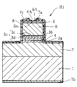
the accompanying drawings. Fig. 2 shows an example B1 of the
surface emitting semiconductor laser device of the present
invention, and Fig. 3 shows another example B2 thereof.
The layer structures of those devices B1 and B2 are the
CA 02347708 2001-04-24
7
same as that of the device A shown in Fig. 1, with an
exception in that a dielectric film is also formed on the
surface of the opening portion 6C which serves as the
aforementioned laser-beam-emerging window 6a of the device A
so that the planar shape of the laser-beam-emerging windows of
the devices B1 and B2 differ from that in Fig. 1.
In the device B1, a dielectric film 8A having a planar
shape of an annular ring is formed at the opening portion
which is located inside an upper electrode 7a, thereby forming
a new beam-emerging window 6A of a smaller diameter which has
a circular planar shape.
In the device B2, a dielectric film 8B having a circular
planar shape is formed at the center portion of a GaAs layer 6
which is exposed through the opening portion 6C, thereby
forming a new beam-emerging window 6B which has a planar shape
of an annular ring.
It is preferable that the thickness of the dielectric
film 8A (8B) be approximately a value of ~ x (2i + 1)/4n
where ~ is the oscillation wavelength of the laser beam
emitted by the device B1 (B2), n is the refractive index of
the dielectric that is the material for the dielectric film 8A
(8B) and i is an integer, such as 0, 1, 2 or the like.
When the dielectric film 8A (8B) having the
aforementioned planar shape and thickness is formed on the
topmost surface, the effective reflectance of the upper
reflector layer structure that is located directly below the
dielectric film 8A (8B) decreases. As a result, laser
oscillation does not occur only directly under the dielectric
film 8A (8B), so that the transverse modes are controlled.
The planar shape of this dielectric film is not limited
to those mentioned above, but may be changed any desirable
shape.
It is preferable that the dielectric film is formed with
a thickness of ~ x 2i/4n, and a metal film of Au, Ti, Cr or
CA 02347708 2001-04-24
8
the like be formed on the dielectric film, because the metal
film enhances the effect of reducing the reflectance so that
control of the transverse modes of the laser beam is
demonstrated more effectively.
As the dielectric film (transparent layer) formed at the
opening portion 6C demonstrates the aforementioned effect, it
is desirable that the forming position of the dielectric film
is included in the planar shape of the current feeding passage
3e that regulates the laser oscillation in a light-emitting
layer 4. This is because the design surely reduces the
effective reflectance of the upper reflector layer structure 5
located directly under the dielectric film with respect to the
laser beam which oscillates through the current feeding
passage 3e, thereby improving the reliability of the control
of the transverse modes.
E
(1) Structures of laser devices
The laser device shown in Fig. 2 was fabricated in the
following manner. Note that the oscillation wavelength of
this laser device is designed to be 850 nm.
A thin layer of n-type Alo.ZGao.eAs with a thickness of 40
nm and a thin layer of n-type Alo.9Gaa,lAs with a thickness of
50 nm were alternately laminated on an n-type GaAs substrate 1
by MOCVD with a composition twisted layer of a thickness of 20
nm intervened at each interface of the heterojunction of both
thin layers, thus forming a lower reflector layer structure 2
having 30.5 pairs of multiple layers. Then, a lower clad
layer 3a (thickness of 97 nm) of non-doped Alo.,Gao.,As, a
light-emitting layer 4 with a quantum well structure, which
comprises a 3-layer GaAs quantum well layer (each layer having
a thickness of 7 nm) and a 4-layer Alo.zGao.BAs barrier layer
(each layer having a thickness of 8 nm) and an upper clad
layer 3b (thickness of 97 nm) of non-doped Alo.3Gao.,As were
stacked in order on the lower reflector layer structure 2.
CA 02347708 2001-04-24
9
Then, a thin layer of p-type Alo.2Gao.8As with a thickness of 40
nm and a thin layer of p-type Alo.BGao.zAs with a thickness of
50 nm were alternately laminated on the resultant structure
with a composition twisted layer of a thickness of 20 nm
intervened at each interface of the heterojunction of both
thin layers, thus forming an upper reflector layer structure 5
having 25 pairs of multiple layers.
Then, a p-type GaAs layer 6 was stacked on the topmost
layer, the p-type Alo.ZGao.BAs layer, of the upper reflector
layer structure 5.
The lowermost layer 3c of the upper reflector layer
structure 5 was formed of p-type AlAs with a thickness of 50
nm.
Next, an Si,N, film 8a was formed on the surface of the
p-type GaAs layer 6 in the layer structure by plasma CVD, and
a circular resist mask 9 having a diameter of about 45 ~,m was
formed on the Si3N, film Sa by photolithography using an
ordinary photoresist (Fig. 4).
Then, the Si,N, film 8a excluding the part lying directly
under the resist mask 9 was etched out by RIE using CF,, after
which the resist mask 9 was entirely removed, thus exposing
the surface of the GaAs layer 6 which has a planar shape of an
annular ring.
Then, with the Si3N, film 8a used as a mask, etching to
the lower reflector layer structure 2 was carried out using an
etchant which is a mixture of phosphoric acid, hydrogen
peroxide and water, thus forming a columnar structure (Fig. 5).
Then, this columnar structure was heated at 400°C for
about 25 minutes in the atmosphere of water vapor. Only the
outer peripheral portion of the p-type AlAs layer 3c was
selectively oxidized into an annular ring shape, forming a
current feeding passage 3e with a diameter of about 15 ~m in
the center portion (Fig. 6).
Next, the Si,N, film 8a was completely removed by RIE,
CA 02347708 2001-04-24
and the entire surface was coated with an Si3N, film 8 by
plasma CVD. Then, the Si3N, film 8 formed on the top surface
of the GaAs layer 6 with a diameter of about 35 ~,m was removed
in an annular ring shape having an outside diameter of 25 ~m
5 and an inside diameter of 15 fan, thus exposing the surface of
the GaAs layer 6. AuZn was then vapor-deposited on the
exposed surface to form an upper electrode 7a having an
annular ring shape. Then, only the outside surface of the
upper electrode 7A was coated with an Si,N~ film 8 on which a
10 pad 7c for an electrode lead was formed of Ti/Pt/Au (Fig. 7).
The thickness of the Si,N, film 8 then was set to 121 nm,
a value acquired for i = 0 in the aforementioned equation of ~,
x ( 2i + 1 ) /4n, because the refractive index of Si3N, was 1. 75
and the oscillation wavelength of the device was 850 nm.
Next, photolithography and RIE were performed on the
Si3N, film located inside the upper electrode 7a to bore a
small circular hole with a diameter of 6 ~m in the center
portion, thus exposing the surface of the GaAs layer 6 with
the other Si3N, film 8A remaining. As a result, a beam-
emerging window 6A was formed, thus completing the device B1
shown in Fig. 2. This is designated as Example 1.
In another example, the beam-emerging window 6A was
formed by setting the diameter of the small hole to 10 ~,m.
This is~designated as Example 2.
A portion SB with a diameter of 6 ~,m was left at the
center portion of the Si3N4 film located inside the upper
electrode 7a and the other portion of the Si3N, film was
entirely removed, thus forming a beam-emerging window 6B
having an annular ring shape with an outside diameter of 15 ~,m
and an inside diameter of 6 ~,m. This completed the device B2
shown in Fig. 3. This device is designated as Example 3.
In the device of any of Examples, the back of the
substrate 1 was polished so that the entire substrate 1 had a
thickness of approximately 100 Eun and AuGeNi/Au was vapor-
CA 02347708 2001-04-24
11
deposited on the polished surface, thus forming the lower
electrode 7b.
For comparison, with the oxidation time for the AlAs
layer 3c set to approximately 30 minutes, the oxidation width
of the AlAs layer 3c was increased to set the diameter of the
current feeding passage 3e to about 5 ~.m and the opening
portion 6C with a diameter of 15 ~.m was formed in the GaAs
layer 6, fabricating the device A shown in Fig. 1 in which
this opening portion 6C served as the beam-emerging window 6a.
This device is designated as Comparative example 1. In the
device of Example 1, the whole Si3N,film located inside the
upper electrode 7a was removed to form an opening portion with
a diameter of 15 Eun, fabricating the device A in which this
opening portion served as the beam-emerging window 6a. This
device is designated as Comparative example 2.
Table 1 below shows the dimensions of the current feeding
passages and the dimensions and shapes of the beam-emerging
windows of the above five types of devices.
Table 1
Diameter Dimension Diameter Shape of bea<n-
of of upper of
columar electrode current emerging window
structure Inside Outside feeding
(~.un) diameterdiameterpa-ssa9e
( ) ( ) (lam)
Example 1 3 5 1 5 2 5 1 5 Circle of 6 Ean
in
diameter
Example 2 3 5 1 5 2 5 1 5 Circle of to
Nm in
diameter
Example 3 3 5 1 5 2 5 1 5 Annular ring
with
outside diameter
of
15 Eun inside
diameter of 6
Emi
Comparative 3 5 1 5 ~ 5 5 Circle of 15
Nm in
Example 1 ~~t~'
Comparative 3 5 1 5 ~ 5 1 5 Circle of 15
Eml in
Example 2 ~~t~'
CA 02347708 2001-04-24
12
(2) Evaluation of characteristics of laser devices
1) Fig. 8 shows the current-voltage characteristics and
current-optical output characteristics of Example 1 and
Comparative example 1. In this diagram, the solid lines
represent the current-voltage characteristics and the broken
lines represent the current-optical output characteristics.
In both Example 1 and Comparative example 1, oscillation
takes place in the fundamental transverse modes.
As apparent from Fig. 8, Example 1 has a lower operation
voltage than Comparative example 1; for example, the former
operation voltage is about 1.8 V at 5 mA which is considerably
lower than the operation voltage of 2.4 V of Comparative
example 1. This is because the diameter of the current
feeding passage of Example 1 is 15 ~,m, making the resistance
there lower than the current feeding passage of Comparative
example 1 which has a diameter of 5 l~ m.
With regard to the current-optical output characteristics,
the optical output of Example 1 is increasing without
saturation until the current becomes about 10 mA even though
the threshold current is slightly high as compared with that
of Comparative example 1. This seems to have resulted from
the effect of suppressing the heat generation due to the low
resistance in the vicinity of the current feeding passage.
2) Fig. 9 shows the current-voltage characteristics and
current-optical output characteristics of Examples 2 and 3 and
Comparative example 2. In this diagram, the solid lines
represent the current-voltage characteristics and the broken
lines represent the current-optical output characteristics.
As apparent from Fig. 9, no significant differences in
both characteristics among Examples 2 and 3 and Comparative
example 2 are seen.
The near-field patterns for the devices of Examples 2 and
3 and Comparative example 2 were observed. Fig. 10 shows the
results of the observation with the operation current of 7 mA,
CA 02347708 2001-04-24
13
and Fig. 11 shows the results of the observation with the
operation current of 15 mA.
In Figs. 10 and 11, a pattern a is for Example 2, a
pattern b is for Example 3 and a pattern c is for Comparative
example 2.
As apparent from Figs. 10 and 11, the pattern c for
Comparative example shows multiple emission spots at the
peripheral portion, which are switched by the feeding of the
current. In the case of the pattern a of Example 2, there are
fewer emission spots which are concentrated at the center
portion. Even increasing the amount of current fed did not
cause any switching action in the latter case.
In the case of the pattern b of Example 3, the number of
emission spots becomes greater than that of Example 2. What
is more, the entire emission spots are scattered. Increasing
the amount of current fed did not cause any switching action
in the case of Example 3 either.
INDUSTRIAL APPLICABILITY
As apparent from the above description, the laser device
of the present invention is a surface emitting semiconductor
laser device capable of controlling the transverse modes, for
example, a laser device which oscillates at a low operation
voltage in fundamental transverse modes. For a laser device
which oscillates in high-order transverse modes, noise caused
by mode switching is reduced. Therefore, this surface
emitting semiconductor laser device can be used as a light
source for parallel data transmission and thus contributes to
constructing a fast optical data communications system.
Further, the transverse modes of the laser device
according to the present invention is controlled by the planar
shape of the dielectric film (transparent layer) formed on the
entire top surface, not by the size of the current
constriction structure. This provides the design of the laser
CA 02347708 2001-04-24
14
device with a higher degree of freedom and facilitates the
fabrication, thus leading to a lower manufacturing cost.