Note: Descriptions are shown in the official language in which they were submitted.
CA 02347890 2001-04-24
WO 00/26739 PCT/US99/25815
HIGH EFFICIENCY POWER SUPPLY FOR A TWO-WIRE LOOP POWERED
DEVICE
Field of the Invention
The present invention relates to the field of instrumentation and control.
More
particularly, the invention relates to a high-efficiency device that draws
power and transmits
a signal over the same conductors.
Background of the Invention
Two-wire transmitters and controllers are well known in the field of
instrumentation and control. Generally, a two-wire transmitter is a low-power
device located
proximate a substance, and used to measure one or more conditions of the
substance (e.g.,
fluid level, temperature, pressure, flow). A two-wire controller is a low-
powered device used
for controlling such conditions (e.g., a remotely operated valve). The
transmitter and
controller uses the same conductors both to receive power from a power source
and to
transmit and/or receive signals to or from one or more indicating and/or
control devices (e.g.,
display, meter, programmable controller, computer).
In order to accomplish these functions, two-wire transmitters and two-wire
controllers traditionally incorporate certain components. Two-wire devices
typically are
coupled to an external power supply by a pair of conductors that form a loop
between the
device and the power supply. Two-wire devices are also coupled to a transducer
device. In
the case of the transmitter, the transducer monitors the conditions to be
measured. The
transducer provides a signal to the transmitter proportional to the condition
of the substance
to be measured. Acting as a variable current sink, the effective series
resistance across the
transmitter varies so as to produce a change in the current drawn by the
transmitter
representative of the condition being monitored. In the case of the
controller, the transducer
CA 02347890 2001-04-24
WO 00/26739 PCT/US99/25815
-2-
controls the state of the condition. The controller provides a signal to the
transducer
proportional to the desired state of the condition.
Current industry standards place certain constraints on the operation of two-
wire devices. One such constraint is that the current in the two-wire loop
must be between
approximately 4 milliamperes and 20 milliamperes under normal operating
procedures.
Moreover, it is desirable that a 4-20 milliampere transmitter be capable of
operating on
slightly less than 4 milliamperes and also be able to draw slightly more than
20 milliamperes
to facilitate calibration. For example, in the case of a transmitter using
HARTTM protocol, a
I milliampere peak-to-peak AC current must be superimposed on the operating
current,
requiring the transmitter to be capable of operating at instantaneous currents
as low as 3.5
milliamperes.
A second constraint requires two-wire devices to be capable of operating from
a standard power supply, usually 24 volts direct current (DC). These power
supplies often
have intrinsic safety barriers which may have an internal resistance of
several hundred ohms.
In addition, two-wire devices often must operate in circuit loops that may
have wire resistance
up to a few hundred ohms. For example, if an indicating device is used, the
total loop
resistance often reaches 600 ohms, thus reducing the terminal voltage at the
two-wire device
to 12 volts DC when the loop current is 20 milliamperes. As a result of this
limited voltage
supply, power available to the two-wire device is severely limited.
A third constraint is that two-wire devices typically contain electronic
circuitry,
which must operate from a reduced voltage (e.g., 3, 5, 10 volts) that cannot
vary as the
available voltage changes. As a result, the transmitter must employ circuitry
to reduce the
voltage available from the loop to the required voltage levels. Because the
amount of power
provided to the circuitry influences its capability, speed and accuracy, the
regulation circuitry
must function with as little power loss as possible.
To date, this regulation process has been performed by a linear regulating
circuit, or by a linear regulating circuit in series with a non-linear
regulating circuit. These
linear regulating circuits unnecessarily reduce the power available to the
circuitry by
dissipating power equal to the product of the current used multiplied by the
difference
between the input voltage and the voltage required to operate the measuring
circuit. For
example, for a measuring circuit operating on 10 volts DC where the
transmitter receives 21
CA 02347890 2001-04-24
WO 00/26739 PCT/US99/25815
-3-
volts DC, the power associated with the additional I 1 volts would be
dissipated in the form
of heat.
Therefore, it is one object of the invention to provide a two-wire device in
which the available power is not reduced as a consequence of the required
power conversion.
Many two-wire devices store energy in order to permit high, intermittent peak
energy use without requiring sudden increases in loop current. When power is
first applied
to the two-wire device, local energy storage devices can cause high loop
current to flow,
called inrush current. Large inrush currents can trigger thyristor-type
intrinsic safety barriers,
and can interfere with digital signaling systems.
Therefore, it is another object of the invention to provide internal energy
storage without causing large inrush currents.
Summary of the Invention
The present invention provides a process control device that does not reduce
the available power during the required power regulation. The process control
device
comprises a measuring circuit and a power regulator circuit. The measuring
circuit, which is
coupled to the power regulator circuit, produces a control signal indicative
of a measured
value. The power regulator circuit is created such that it does not limit
available power to the
measuring circuit. The process control device also may comprise a power
control circuit
coupled to the measuring circuit. The power control circuit redirects a
portion of the available
power from the power regulator circuit in proportion to the control signal
produced by the
measuring circuit. The process control device also comprises two or more
conductors that are
in electrical communication with the power regulator circuit and the power
control circuit.
These conductors deliver the available power to the power regulator circuit
and the power
control circuit, as well as receiving a first electric signal from the power
regulator circuit and
a second electric signal from the power control circuit. The first and second
electric signal
may be electric currents, whose combined value falls in the range of 4-20
milliamperes. In
addition, the available power may be provided by a direct-current power
source.
The power regulator circuit may comprise a non-linear, power regulator, for
example, a switching regulator. The power control circuit may comprise a
voltage to current
converter. The control signal provided by the measuring circuit may be an
electric voltage,
CA 02347890 2007-02-21
63189-483
-4-
and the measured value may be provided to the measuring
circuit by a sensor, for example a transducer. The power
regulator circuit may also comprise a current limiting
circuit for reducing current surges present when the process
control device begins to operate.
According to an aspect of the invention, a method
is provided for use in a process control system. The method
comprises receiving power, regulating the power with a power
regulator circuit to a first value to operate a measuring
circuit, providing to a power control circuit a control
signal produced by the measuring circuit, and converting the
control signal to an electric signal to operate an indictor.
Notably, the power regulator circuit does not limit the
power to the measuring circuit.
According to an aspect of the invention, a process
control system is provided. The process control system
comprises a sensor adapted to determine a measured value, a
process control device (as described above) in electrical
communication with the sensor, and a power source coupled to
the process control device by two or more conductors. The
conductors deliver the available power from the power source
to the process control device, and receive an electric
signal from the process control device. The process control
system further comprises an indicating device for describing
the electric signal. The indicating device is coupled to
the power source and the process control device.
According to one aspect of the present invention,
there is provided a process device, comprising: a measuring
circuit that produces a control signal indicative of a
measured value; a power regulator circuit coupled to said
measuring circuit such that said power regulator circuit
does not limit available power to said measuring circuit;
CA 02347890 2007-02-21
63189-483
-4a-
and two or more conductors in electrical communication with
said power regulator circuit, wherein said conductors
deliver said available power to said power regulator
circuit, and wherein said conductors receive a first
electric signal from said power regulator circuit.
According to another aspect of the present
invention, there is provided a method for use in a process
control system, comprising: receiving power; regulating
said power with a power regulator circuit to a first value
to operate a measuring circuit, wherein said regulation does
not limit said power to said measuring circuit; and
providing a first control signal produced by said measuring
circuit to operate an indicator.
According to still another aspect of the present
invention, there is provided a process control system,
comprising: a sensor adapted to determine a measured value;
a process control device in electrical communication with
said sensor, comprising: a measuring circuit that produces
a control signal indicative of said measured value; and a
power regulator circuit coupled to said measuring circuit
such that said power regulator circuit does not limit
available power to said measuring circuit; a power source
coupled to said process control device by two or more
conductors, wherein said conductors deliver said available
power from said power source to said process control device,
and wherein said conductors receive an electric signal from
said process control device; and an indicating device
coupled to said power source and said process control
device, wherein said indicating device describes said
electric signal.
CA 02347890 2007-02-21
63189-483
-4b-
Brief Description of the Drawings
Figure 1 is a block diagram of a two-wire
transmitter and controller system according to the present
invention;
Figure 2 is a block diagram of a two-wire
transmitter device according to the present invention;
Figure 3 is a graph of the power conserved by
using a non-linear power converter circuit in the two-wire
device;
Figure 4 is a schematic diagram of a preferred
embodiment of a high-efficiency non-linear regulator
circuit;
Figure 5 is a schematic diagram of a preferred
embodiment of a current limiting circuit;
Figure 6 is a schematic diagram of an output
amplifier circuit;
CA 02347890 2001-04-24
WO 00/26739 PCTIUS99/25815
-5-
Figure 7 shows another embodiment of the present invention using a
transformer device in the two-wire transmitter device; and
Figure 8 is a block diagram of a two-wire controller according to the present
invention.
Detailed Description of Preferred Embodiment
As shown in Figure 1, a two-wire system may include a two-wire
transmitter 10 and a two-wire controller 24. Two-wire transmitter 10 is
coupled to a
programmable controller 32 by conductors 13 and 14, which are connected to
terminals 15
and 16 of two-wire transmitter 10. Two-wire controller 24 also is coupled to
programmable controller 32 by conductors 25 and 26. Programmable controller is
further
coupled to a power supply 1 l by conductors 33 and 34. Power supply 11
provides a
voltage V;,,, preferably in the range of 12-40 volts direct-current (DC), more
preferably 24
volts DC.
Two-wire transmitter is also coupled to a load represented by resistor 12.
Resistor 12 represents one or more indicating devices, including power meters,
visual
displays, and HARTT"" communication devices. Although the value of resistor 12
will vary
depending on the type and quantity of indicating devices, a 600 ohm load is an
industry-
accepted approximation. Therefore, a voltage drop Vd, results across resistor
12, leaving a
voltage Vt at terminals 15 and 16 of two-wire transmitter 10. The value of
voltage drop
Vd,, and thus of terminal voltage V, will depend on the value of loop current
I.
Transmitter 10 is adapted to draw loop current I, in the range of 4-20
milliamperes, in
accordance with industry-standard indicating devices. The value of loop
current Ii at any
particular instant is dependent upon a signal received by transmitter 10 from
a transducer
17.
Two-wire transmitter 10 is coupled to transducer 17 through conductors 18
and 19 connected to terminals 20 and 21 of two-wire transmitter 10. Transducer
17
monitors a condition (e.g., level, temperature, pressure) of a substance 22,
located in tank
23. As the monitored condition changes, transducer 17 sends a signal St to two-
wire
transmitter 10. In accordance with the received signal Sõ two-wire transmitter
10 adjusts
the amount of current it draws from power supply 11 in accordance with a
predetermined
CA 02347890 2001-04-24
WO 00/26739 PCT/US99/25815
-6-
setting. Industry-standard two-wire transmitters commonly draw 4 milliamperes
when the
monitored condition is at its lowest point (e.g., empty tank) and 20
milliamperes when the
monitored condition is at its highest point (e.g., full tank). Accordingly,
when signal St
from transducer 17 indicates a low-point condition, two-wire transmitter 10
will draw 4
milliamperes, and when signal St from transducer 17 indicates a high-point
condition, two-
wire transmitter 10 will draw 20 milliamperes.
Programmable controller 32 provides a logic interface between two-wire
transmitter 10 and two-wire controller 24.. As transducer 17 monitors the
level of
substance 22 in tank 23, two-wire transmitter 10 varies loop current I, (as
discussed above).
In accordance with the value of loop current I,, programmable controller 32
provides a
voltage signal to two-wire controller 24. Two-wire controller 24 measures
voltage
available in a loop formed by conductors 25 and 26. Two-wire controller 24
then sends a
signal to transducer 27 on conductors 29 and 28. Transducer 27 may then
operate to adjust
the level of substance 22 in tank 23. For example, transducer 27 may operate a
valve (not
shown) that opens a fill pipe 30 and allows tank 23 to receive additional
substance 22
through supply pipe 31.
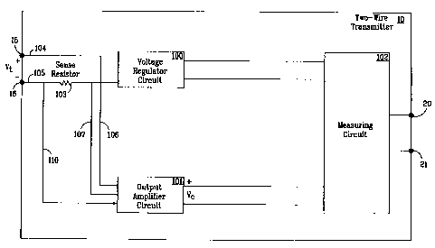
Figure 2 shows a block diagram of two-wire transmitter 10. Two-wire
transmitter 10 comprises a voltage regulator circuit 100, an output amplifier
circuit 101,
and a measuring circuit 102. Voltage regulator circuit 100 and output
amplifier circuit 101
couple directly to terminal 15 of two-wire transmitter 10, and couple through
a sense
resistor 103 to terminal 16 of two-wire transmitter 10. In addition, voltage
regulator circuit
100 and output amplifier circuit 101 are coupled to measuring circuit 102.
Measuring
circuit 102 is coupled to terminals 20 and 21 of two-wire transmitter 10.
When measuring circuit 102 receives signal S, from transducer 17 (as shown
in Figure 1), measuring circuit 102 provides an output control voltage Vc to
output
amplifier circuit 101. Output amplifier circuit 101 acts as a variable load
and draws a
portion of loop current I, (as shown in Figure 1) on conductor 106 in
proportion to the
value of output control voltage V,. The precise value of the portion of loop
current I1
drawn by output amplifier circuit 101 depends on the amount of loop current I,
drawn by
voltage regulator circuit 100. For example, using a 70 milliwatt measuring
circuit
operating at 10 volts DC and 7 milliamperes, a 20 milliampere loop current I1
will cause
CA 02347890 2001-04-24
WO 00/26739 PCT/US99/25815
-7-
voltage regulator circuit 100 to draw 6.13 milliamperes. Therefore, in order
to maintain
the 20 milliampere loop current Ii, output amplifier circuit 101 will draw the
remaining
13.87 milliamperes.
Because terminal voltage V, varies with loop current I,, two-wire transmitter
10 employs voltage regulator circuit 100 to provide a constant voltage and
constant current,
necessary to operate measuring circuit 102. Preferably, for a 70 milliwatt
measuring
circuit 102, a constant voltage of 10 volts DC and a constant current of 7
milliamperes is
provided by voltage regulator circuit 100 to measuring circuit 102.
Non-linear circuits regulate voltage and current more efficiently than linear
regulator circuits, and thus non-linear regulators do not limit the power
available to
measuring circuit 102 across the entire 4-20 milliamperes range of permitted
loop currents.
Figure 3 is a graph illustrating power available to measuring circuit 102
(left vertical axis),
loop current I, (horizontal axis), and terminal voltage V, (right vertical
axis) at two-wire
transmitter 10 (as shown in Figure 1). Figure 3 shows a curve 301 representing
power
available with a non-linear regulator, a line 302 representing power available
with a linear
regulator, and a line 303 indicating the value of terminal voltage Vt.
Considering one
example when loop current 11 is 4 milliamperes and terminal voltage V, is 21.6
volts, the
linear regulator circuit dissipates 40.6 milliwatts of power, thus providing
45.8 milliwatts
to measuring circuit 102. However, at the same loop current I1 of 4
milliamperes and the
same terminal voltage V, of 21.6 volts, a 95% efficient non-linear regulator
circuit
dissipates just 1.75 milliwatts of power, thus providing 85.65 milliwatts of
power to
measuring circuit 102. Although this graph represents available power for a 24
volt power
supply and a 600 ohm series resistance, it should be appreciated that non-
linear regulators
are more efficient than linear regulators independent of the power supplied or
the series
resistance.
The additional power available with a non-linear regulating circuit permits
measuring circuit 102 to have an increased capacity. For example, with a 24
volt power
supply and a 600 ohm series resistance, a non-linear regulator with a 95%
power efficiency
will permit the use of a 70mW measuring circuit. A linear regulating circuit,
on the other
hand, only permits the use of a 35mW measuring circuit for the same 24 volt
power supply
and 600 ohm series resistance. As compared to the 35mW measuring circuit, the
70mW
CA 02347890 2001-04-24
WO 00/26739 PCT/US99/25815
-8-
measuring circuit has increased capabilities including the ability to measure
a broader
range of condition values (e.g., larger fluid depths) and the ability to
provide faster and
more accurate measurements to the indicating devices.
Figure 4 is a detailed schematic of a preferred embodiment of a high
efficiency
non-linear regulator circuit 100. In this circuit, power is transferred to an
inductor 400
whenever the gate of transistor 401 goes low. While the gate of transistor 401
is allowing
current to flow through inductor 400, regulated voltage 402 rises. Energy is
stored in inductor
400 and returned to the load through Schottky diode 429 when transistor 401 is
off. When
regulated voltage 402 reaches a set point, the gate of transistor 401 will
turn off and non-linear
regulator circuit 100 will draw the needed power from inductor 400, causing
regulated voltage
402 to begin to decrease. When regulated voltage 402 decreases below a lower
set point, the
gate of transistor 401 will again turn on, and the above cycle will be
repeated. Inductor 400
is switched rapidly from supply line 403 by transistor 401 to common terminal
430 by
Schottky diode 429.
Resistors 427 and 428 bias the base of transistor 422 at one-third of the
voltage
at terminal 402. Resistors 425 and 426 charge capacitor 424 until voltage on
the emitter of
transistor 422 rises one-half volt above its base, thus allowing transistor
422 to conduct. As
the voltage on the emitter of transistor 422 rises, current through transistor
422 increases until
transistor 423 conducts. Increasing current through transistor 423 causes an
increasing voltage
drop across resistors 426 and 431. Because resistors 426 and 431 are coupled
by capacitor 432
to the base of transistor 422, current through transistor 422 rises rapidly,
saturating transistors
422 and 423. Voltage on the emitter of transistor 422 is clamped to voltage at
the base of
transistor 423 (approximately 0.6 volts). When capacitor 432 has discharged,
voltage at the
base of transistor 422 begins to rise. Capacitor 424 prevents the voltage at
the emitter of
transistor 422 from rising as quickly as the base, thus causing transistors
422 and 423 to turn
off. The process then repeats, producing an approximately 4 volt sawtooth
wave.
One requirement for non-linear regulator circuit 100 is that DC voltage 402
preferably is maintained at 9.45 volts. Operation amplifier 404 achieves this
requirement.
Operational amplifier 404 compares voltage on diode 405 with that of voltage
divider formed
by resistors 406, 407, 433, and 408. Capacitor 434 provides a zero voltage in
a closed-loop
response to partially cancel one of the poles from the filter formed by
inductor 400 and
CA 02347890 2001-04-24
WO 00/26739 PCT/US99/25815
-9-
capacitors 420 and 421. Resistor 433 provides negative feedback, limiting the
gain and
maintaining control loop stability. Non-linear regulator circuit 100 is
designed so that the
output of operational amplifier 404 will vary from 1 volt, when voltage at
terminal 402 is 9.56
volts, to 6 volts when the voltage at terminal 402 is 9.5 volts.
Resistor 416, capacitor 417, and transistor 411 perform a comparator function.
When voltage at the source of transistor 411 is more positive than threshold
voltage at its gate,
transistor 411 is turned off. Transistor 411 begins to conduct when voltage at
its source is less
positive than the threshold voltage at its gate. At this point, its current is
being limited to less
than 90 microamperes by reference diode 435, resistors 413 and 436, transistor
414. Capacitor
417 provides a low impedance source for the pulsating current flow of
transistor 411. Resistor
416 isolates capacitor 417 from operational amplifier 404.
Resistors 419 and 437, and transistor 412 drive transistor 401. Current pulses
from transistor 411 saturate transistor 412, shorting the gate drive to
transistor 401. When
transistor 412 turns off, resistor 437 pulls the gate of transistor 401 down
to conunon terminal
430. Because voltage across resistor 437 is several times the threshold
voltage of transistor
401, transistor 401 turns on rapidly. Similarly, a rapid turn-off of
transistor 401 is assured by
the low impedance of saturated transistor 412, thus minimizing switching
losses. Schottky
diode 429 provides a low loss path for inductor 400 to supply current when
transistor 401 turns
off. Capacitors 438 and 415 provide a low impedance source of current to
transistor 401.
Similarly, capacitors 420 and 421 provide a low impedance over a wide
frequency range to
filter the output of non-linear regulator circuit 100.
Because operation amplifier 404 must sink almost all current that flows
through
transistor 411, transistor 412 can not be turned on until the supply is
regulating. Therefore,
the supply is self-starting.
It is desirable to use transistor 401, where transistor 401 is set such that
its
maximum permissible gate voltage exceeds the maximum supply voltage to the
device.
However, if this cannot be accomplished, an optional gate voltage limiter
comprising an
avalanche diode 440 in series with a switching diode 439 may be added.
Switching diode 439
isolates the gate voltage from the high capacitance of avalanche diode 440,
thus preventing
it from slowing down the drive wave while still protecting the gate.
CA 02347890 2001-04-24
WO 00/26739 PCT/US99/25815
-10-
Figure 5 is a schematic diagram of a preferred embodiment ofa current limiting
circuit 500, which is an integral part of voltage regulator circuit 100.
Generally, current
limiting circuit 500 is used at startup to ensure that inrush current does not
exceed the
specifications of a given system. At start-up, depletion-mode transistor 506
becomes saturated
and turns on transistor 507. Voltage on conductor 518 increases as does
voltage on conductor
519 until transistor 505 is turned on. As a result, current flows through
resistor 516 into zener
diode 504 and starts turning off transistor 506. Transistor 506 thus acts as a
source follower
amplified by transistor 507 to maintain the voltage on conductor 518 at
approximately 7 volts.
Transistor 505 becomes saturated and maintains a voltage on conductor 520,
thus maintaining
the voltage on conductor 520 at approximately the same voltage as the common
on conductor
521. Negative input 509 of operational amplifier 501 is held at the same
voltage as conductor
520, while the voltage at positive input 510 of operational amplifier 501 is
biased between the
voltage at terminal 522 (-loop) and the voltage on conductor 519 by voltage
divider resistors
502 and 503.
As long as a current drawn by two-wire transmitter 10 is too small to cause a
voltage across current sensing resistor 103 to approach the product of the
voltage across zener
diode 504 multiplied by the ratio of resistor 503 to resistor 502, voltage at
positive input 510
of operational amplifier 501 will be positive with respect to a voltage at
conductor 521. As
a result, output 512 of operational amplifier 501 will be high, thus turning
on transistors 523
and 513. However, if a current drawn by two-wire transmitter 10 becomes large
enough to
cause a voltage at positive input 510 of operational amplifier 501 to approach
the voltage on
conductor 520, operational amplifier 501 will enter its active region, thus
reducing the voltage
at the gate of transistor 523 and reducing a current through resistors 524,
525, and 526. The
decrease in voltage across resistor 526 will bring transistor 513 out of
saturation. As a result,
current drawn by the remaining circuitry of two-wire transmitter 10 will be
limted, and the
voltage at positive input 510 of operational amplifier 501 will be
approximately equal to the
voltage on conductors 520 and 521. Thus, current drawn by two-wire transmitter
10 is held
at a predetermined level (as determined by Zener diode 504 and resistors 103,
502, and 503)
until current required by two-wire transmitter 10 decreases below the
predetermined limit.
When the voltage on termina1527 rises to one-half volt above the voltage at
conductor 518, diode 514 begins to conduct. As a result, the voltage at
conductor 518 is one-
CA 02347890 2001-04-24
WO 00/26739 PCT/US99/25815
-11-
half volt below terminal 527. Because the voltage at the gate of transistor
506 is limited by
Zener diode 504, transistor 506 is turned off as is transistor 507. Therefore,
current limiting
circuit 500 is powered from the high-efficiency voltage regulator circuit 100,
exclusively.
The predetermined limiting current is calculated as:
I1im;, = Vref * R503/(R103*R502), where Vref is Zener diode voltage, and the
R103, R502, and
R503 are resistances of resistors 103, 502, and 503, respectively. It is
desirable to make I,;m;t
sufficiently smaller than 20 milliamperes, in order to prevent the worst-case
startup current
from exceeding that level. It is, however, necessary for the loop current to
be able to exceed
20mA in normal operation to facilitate calibration (as discussed above). This
is achieved by
applying a positive voltage at terminal 528 after normal operation is
achieved. This turns on
transistor 515, thus turning off transistor 505. As a result, the voltage on
conductor 520 rises
until it approaches the voltage on conductor 518. The voltage on conductor 519
will also rise
until it is sufficiently less than the voltage on conductor 518 in order to
limit the conduction
of transistors 506 and 507. With no power supplied to operational amplifier
501, its output
512 becomes an open circuit. Resistor 529 pulls up the gate of transistor 523,
which in turn
saturates transistor 513.
If needed, current limiting circuit 500 can be disabled by a signal at the
gate of
transistor 515 which will cause transistor 505 to turn off. Turning off
transistor 505 causes
circuit common 511 to be removed from current limiting circuit 500, and thus
from the
remainder of the two-wire transmitter circuitry. Once circuit common 511 is
removed
transistor 506 will turn off because a voltage divider forms between resistors
508 and 516.
With transistor 506 off, transistor 507 will also be off. Resistor 517 then
discharges the base
of transistor 507 allowing for a quick turn off.
Figure 6 is a detailed schematic of a common output amplifier circuit 404
well-known in the art. Operational amplifier 601 monitors current across the
sense resistor
103. When the voltage on positive tenmina1602 of operational amplifier 601 is
greater than
the voltage across the sense resistor 103, operational amplifier 601 biases
transistor 603
such that current will travel from supply line 403. Transistor 604 is always
on when
transistor 603 is on, because the base of transistor 604 is connected to
regulated voltage
402.
CA 02347890 2001-04-24
WO 00/26739 PCT/US99/25815
-12-
Figure 7 shows another embodiment of the present invention using a
transformer 701. In this case, there are two power supplies (not shown) that
are switched
depending on loop voltage. When the loop current I, (shown in Figure 1)
increases,
terminal voltage V, decreases, and power is drawn through main power switch
702.
Because the input voltage is close to the clamped voltage little power is
wasted when the
loop current drops and input voltage rises and the power is drawn through
booster switch
703 into transfonmer 701. For example with a 24 volt supply and a 500 ohm
series
resistance, when the transmitter is signaling 4 milliamps terminal voltage Vt
would be
approximately 20 volts. Therefore, if transformer 701 has two-to-one turn
ratio of two, the
voltage into measuring circuit 102 would be 10 volts and the current would be
7
milliamperes, for a total power of 70 milliwatts. Switch 702 may be an
enhancement
mode transistor, while switch 703 may be a depletion mode transistor, such
that only one
pre-regulator is on at startup. Operational amplifiers (not shown) could
control the
switching of the two pre-regulators by measuring the voltage across current
sensing resistor
103. A switching power supply 704 would be a preferred to supply power.
Figure 8 shows a block diagram of two-wire controller 800. Two-wire
controller 800 comprises a voltage regulator circuit 801 and a transducer
driver circuit 802.
Voltage regulator circuit 801 couples directly to terminal 804 of two-wire
controller 800,
and couples through a sense resistor 805 to terminal 803 of two-wire
controller 800. In
addition, voltage regulator circuit 801 is coupled to transducer driver
circuit 802.
Transducer driver circuit 802 is coupled in parallel to sense resistor 805.
Transducer
driver circuit 802 also is coupled to terminals 806 and 807 of two-wire
controller 800.
When two-wire controller 24 receives a signal from programmable
controller 32 (as shown in Figure 1), transducer driver circuit 802 measures a
corresponding voltage Vr across sense resistor 805. Transducer driver circuit
802 receives
power from voltage regulator circuit 801, which as described for two-wire
transmitter 10
above, comprises a non-linear regulator. Because non-linear circuits regulate
voltage and
current more efficiently than linear regulator circuits, more power is
available to transducer
driver circuit 802. Accordingly, transducer driver circuit 802 has an
increased capacity for
responding to measured voltage V, across sense resistor 805.
CA 02347890 2001-04-24
WO 00/26739 PCT/US99/25815
-13-
Those skilled in the art will recognize that while a preferred embodiment of
the invention has been fully disclosed and described, improvements and
modifications are
possible without departure from its essential spirit and scope, and still
continue to fulfill
the needs of the art and objects of the invention described above. The scope
of the
invention should therefore not be construed as limited by the preceding
exemplary
disclosure, but only by the following claims.