Note: Descriptions are shown in the official language in which they were submitted.
CA 02348140 2004-O1-19
L-12654
POWER SUPPLY FOR ELECTRIC ARC WELDING
The present invention relates to the art of electric arc welding and more
particularly to a
power supply for electric arc welding with an AC arc current.
The power supply constructed in accordance with the present invention is used
to create a
positive and negative current pulses having high magnitude generally exceeding
1,000 amperes. The
individual pulses are created by a pulse width modulator operating switches in
accordance with
standard practice. Since the switches must change polarity at high voltages,
the power supply is
constructed to cause switching from one polarity to the next opposite polarity
at reduced current
levels. The technique is disclosed in prior application Serial No. 233,235
filed January 19,1999 for
a different type of current pulse.
A technique for providing alternating polarity in an inverter power supply for
pipe welding is shown in Stava 6,051,810.
BACKGROUND OF INVENTION
In the manufacture of pige that has a welded seam, it is common to use
multiple AC welding
arcs at extremely high current levels, such as over 1,000-2,000 amperes. The
less expensive power
supply to create such ultra high welding currents is a transformer based
welder having a sinusoidal
output current. This power supply requires only a large, heavy transformer and
related control
circuitry. However, to accomplish high welding currents the sinusoidal output
has an extremely high
peak current compared to the heating current determined by the root mean
square of the sinusoidal
wave. This relatively inexpensive power supply can create the necessary high
current, but results
CA 02348140 2001-05-17
L-12654
in peak currents that seriously affect the welding operation. To overcome the
disadvantages of a
sinusoidal type electric arc welder, it is now common practice to use power
supplies based upon high
frequency switching technology. These switching type power supplies rectify
the incoming line
voltage to produce a DC link. This DC link is switched through a primary
winding of an output
transformer as alternating pulses to create an output current constituting the
AC arc welding current.
Pulse width modulators determine the frequency in the primary winding of the
output transformer.
' Consequently, the pulses at the output transformer are substantially square
waves. Thus, the root
mean square of the secondary current is essentially the same as the maximum
output current for the
power supply. In this manner, welding arc does not require high peak currents
to obtain the desired
root mean square current for heating. Consequently, the inverter type power
supply overcomes the
disadvantage of the sinusoidal power supply when performing high current
electric arc welding of
the type needed for seam welding pipes. For this reason, pipe welding has been
converted to the
inverter technology.
Even though widely used for pipe welding, inverters present a dilemma.
Standard inverter
type power supplies generally have a maximum output in the range of 500
amperes. To provide an
inverter type power supply for high currents in excess of 1,000-2,000 amperes,
a special inverter
must be designed and engineered. This involves substantial costs and highly
trained electrical and
welding engineers. But, such high capacity power supply has a relatively low
sales volume.
Consequently, high current inverters for use in pipe welding are not
economically feasible and
demand a long lead time. To overcome these disadvantages, The Lincoln Electric
Company has
developed a power supply using a master inverter, with one or more slave
inverters controlled and
-2-
CA 02348140 2001-05-17
L-12654
operated in unison. When the welding operation requires a current in excess of
1500 amperes, three
inverters are parallel. The rated output current for the compound inverter is
tripled over a single off-
the-shelf inverter. Increasing the number of inverters operated in unison to
provide a high current
type welder is expensive, but accomplishes the desired results.
There is a need for a high current power supply that creates an AC welding
current having
a root mean square current of over 1,000-2,000 amperes without the requirement
of paralleling
.several standard low current inverters. Such high current power supply for
use in electric arc
welding of pipes must not have the peak current problem, experienced by a
sinusoidal type power
supply.
THE INVENTION
The present invention relates to an improved power supply for high current, AC
electric arc
welding, which power supply can be used in the field for pipe welding and
other high current
applications. A transformer converts AC line voltage, such as single phase or
three phase line
voltage, to a low output AC voltage, such as 70-100 volts. The output voltage
is rectified and drives
two standard down chopper modules, each driven by a common pulse width
modulator. In some
instances, each module may be driven by a dedicated pulse width modulator. A
somewhat standard
control board with a microprocessor controller sets the pulse width and,
therefore, the magnitudes
of the positive and negative current pulses constituting the AC welding
current. This relatively
inexpensive power supply can replace large inverter units without substantial
engineering and lead
time. The only disadvantage of the present invention is its high weight, due
to the large input
transformer; however, such weight is not a serious problem in pipe welding or
other high current
-3-
CA 02348140 2001-05-17
L-12654
applications. By using the present invention, the power supply is robust and
simple to construct.
The power supply is constructed with readily available components.
In accordance with the present invention there is provided a power supply
connectable to a
source of AC line voltage for AC electric arc welding by an AC arc current
across a gap between the
electrode and workpiece. The electrode is in the form of an advancing wire
that is melted by the arc
and deposited on the workpiece. In practice, the workpiece is the gap or joint
between two pipe
. sections. Line voltage is single, or three phase with a voltage between 200
volts and 600 volts AC.
The frequency is normally 50 hertz or 60 hertz. The inventive power supply
uses a high capacity,
large transformer to convert line voltage to an AC output voltage of less than
about 100 volts AC.
A rectifier converts the AC output voltage to a DC voltage. This DC voltage
has a positive potential
at a first terminal and a negative potential at a second terminal. The third
common terminal is at
substantially zero voltage. This zero voltage terminal is preferably a system
ground for the rectifier
and welding operation. However, the common terminal can be the junction
between two generally
equal capacitors connected in series across the positive and negative
terminals of the rectifier. This
common terminal, or junction, coacts with the positive and negative terminals
of the rectifier to
provide DC voltage, either positive or negative. A network includes a first
switch for connecting
the positive terminals to the common terminal and across the gap when a gate
signal is applied to
the first switch and a second switch for connecting the negative terminal to
the common terminal and
across the gap when a gate signal is applied to the second switch. A pulse
width modulator generates
the gate signal in the form of pulses with a pulse frequency of at least about
18 kHz. A first logic
gate directs the gate signal to the first switch for a first time period, i.e.
a positive current portion,
-4-
CA 02348140 2001-05-17
L-12654
and a second logic gate directs the gate signal to the second switch for a
second time, i.e. a negative
current portion. A controller alternately operates the logic gates to create
an AC arc current
alternating between the opposite polarity current portions. The time of the
first switch, i.e. the
positive portion, can be different than the time of the second switch, i.e.
the negative portion. In
addition, the duty cycle of the pulse width modulator can be different during
the first time, than
during the second time. This produces a different amplitude for the alternate
positive and negative
' portions or current pulses creating the AC arc current across the welding
gap. The arc melts the
advancing wire electrode to deposit molten metal onto the workpiece which, in
practice, is a pipe
seam.
In accordance with another aspect of the present invention, the controller for
the power
supply includes an output terminal at which is created a switch enabling
signal having a first logic
during the first time, i.e. positive or negative output current and a second
logic during the second
time, i.e. opposite current polarity. There are means for directing the pulses
from the pulse width
modulator to the first switch during the first time and then to the second
switch during the second
time. In accordance with still a further object of the present invention,
there is provided a bi-
directional, but selectable, free wheeling circuit in parallel with the
welding gap. This circuit is
either a parallel arrangement circuit or a series circuit. In either design,
the diodes are selectively
activated during the first and second time periods. These selectable free
wheeling diodes are located
on the inboard side of the inductor in the output circuit of the welder. As an
alternative, a center
tapped inductor is used for the controlled inductive impedance. In this
architecture, the free
wheeling diode circuits are located on opposite ends of the center tapped
inductor or choke.
-5-
CA 02348140 2001-05-17
L-12654
The primary object of the present invention is the provision of a power supply
capable of
creating high current AC welding current utilizing relatively inexpensive, low
engineered
components.
Yet another object of the present invention is the provision of a power
supply, as defined
above, which power supply has a root mean square heating capacity, without the
peak currents
associated with sinusoidal power supplies.
Still a further object of the present invention is the provision of a power
supply, as defined
above, which power supply obtains the advantage of parallel mounted inverters,
or large high cost
inverters without the expense and complexity or such paralled inverters.
Yet another object of the present invention is the provision of a power
supply, as defined
above, which power supply provides the simplicity of a down chopper while
obtaining an AC
welding current.
These and other objects and advantages will become apparent from the following
description
taken together with the accompanying drawings.
BRIEF DESCRIPTION OF DRAWINGS
FIGURE 1 is a wiring diagram illustrating the preferred embodiment of the
present invention;
FIGURE lA is a logic diagram showing a portion of the control circuit used in
FIGURE 1;
FIGURE 2 is a partial wiring diagram of a modification in the bidirectional
free wheeling
circuit of the preferred embodiment of the present invention;
FIGURE 3 is a pulse graph of the pulses directed to the welding operation for
balanced
amplitude and equal width of the opposite polarity current portions;
-6-
CA 02348140 2001-05-17
L-12654
FIGURE 3A is a current graph resulting from the pulse graph in FIGURE 3;
FIGURE 4 is a pulse graph similar to FIGURE 3 with a lower amplitude for each
of the
welding portions;
FIGURE 4A is a current graph of the resulting current from the pulse graph
shown in
FIGURE 4;
FIGURE 5 is a pulse graph illustrating different amplitudes for the positive
and negative
current portions of the AC welding current;
FIGURE 5A is a current graph of the resulting current created by the pulse
graph of FIGURE
5;
FIGURE 6 is a pulse graph illustrating current pulses of different magnitude
and pulse width
for the opposite polarity welding current portions; . .
FIGURE 6A is a current graph of the resulting current from the pulse graph
shown in
FIGURE 6;
FIGURES 7-9 are alternative embodiments of the invention, as illustrated in
FIGURE 1;
FIGURE 10 is a combined block diagram and wiring diagram of an earlier power
supply;
FIGURE l0A is a current graph illustrating the AC welding current of one stage
in the power
supply shown in FIGURE 10;
FIGURE lOB is a current graph showing the combined output AC welding current
obtained
in the power supply shown in FIGURE 10;
FIGURE 11 is a wiring diagram illustrating a very simple power supply for
creating high
current as used in pipe welding;
CA 02348140 2001-05-17
L-12654
FIGURE 11A is a sine wave output of the prior art power supply shown in FIGURE
11 at
a medium output current of 500 amperes;
FIGURE 11B is a sine wave output of the prior art power supply shown in FIGURE
11 with
a high AC welding current with a peak of 1,500 amperes;
FIGURE 12 is a pulse diagram showing a further modification of the invention
using
graduated current reduction at the end of each current portion of the welding
current; and,
FIGURE 13 is a representation of a single gate pulse illustrating the gradual
reduction in
width used in the modification of FIGURE 12.
PREFERRED EMBODIMENTS
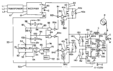
Referring now to the drawings wherein the showings are for the purpose of
illustrating
preferred embodiments of the invention only, and not for the purpose of
lirriiting same, FIGURE 1
shows a high frequency inverter power supply A for developing an output AC
welding current of at
least 1,000-2,000 amperes across the welding gap between electrode E and
workpiece W which, in
practice, is the joint between two adjacent pipe sections J, K. In accordance
with standard practice,
inductor C having an inductive impedance which smooths out the current flow
through the welding
operation defined by electrode E and workpiece W. Electrode E is an advancing
wire from supply
reel R which is melted by the arc created by the AC welding current. Workpiece
W, comprising pipe
sections J, K, is connected to system ground G. This ground is a zero voltage
rail or bus to define
the positive and negative current portions. The AC current in the welding
operation is detected or
sensed through a shunt S to create a current feedback signal that controls the
magnitude of the
welding current. In the illustrated embodiments, power supply A includes a
transformer 10 having
_g_
CA 02348140 2001-05-17
L-12654
an input connected to line voltage shown as a three-phase line voltage. The
line voltage has a
frequency of 50 Hz or 60 Hz. This low frequency and high capacity makes
transformers relatively
large. It creates at least about 40-50 kw of energy. The output of the
transformer produces an output
voltage of less than100 volts AC. The input line voltage varies between 220-
600 volts AC. The
output voltage of transformer 10 is directed to rectifier 12 having a positive
terminal 20, a negative
terminal 22, and a zero voltage terminal 24. Preferably the zero voltage
reference is system ground
G. Positive terminal 20 is connected to power lead 30, whereas negative
terminal 22 is connected
to power lead 32. Positive switch 40 in the form of a FET or IGBT includes an
anti-parallel diode
40a in parallel with a snubber 40b and controlled by a given logic on gate
40c. Logic on the gate 40c
renders the positive switch conductive. The lack of the logic or voltage on
gate 40c turns positive
switch 40 off. In a like manner, there is a negative switch 42, having an anti-
parallel diode 42a in
parallel with a snubber 42b and controlled by a given logic on gate 42c. The
logic or voltage on
gates 40c, 42c control the conductivity of power switches 40, 42,
respectively. These switches are
operated alternately at a frequency desired for the AC welding current. When
switch 40 is
conductive, a positive current flows through inductor C across the gap and to
ground terminal 24 of
rectifier 12. Negative switch 42 causes current flow from ground G in the
reverse direction through
the welding gap and through inductor C. By alternating between operation of
switch 40 and switch
42, an AC current is created in the welding gap between the electrode and the
workpiece.
In accordance with the invention, the switches 40, 42 are enabled for a period
of time during
which the switch itself is rapidly switched between conduction to non-
conduction to direct high
frequency pulses from terminals 20 or 22 through the welding operation. Switch
40 is on for the first
-9-
CA 02348140 2001-05-17
L-12654
time and then switch 42 is on for a second time, i.e. the negative portion. By
definition the "first
time" can be either the positive or negative operation. By switching between
these first and second
times, the frequency of the AC welding current is controlled. The magnitude of
the current is
determined by the amount of current allowed to flow during the first time and
the second time. To
control this operation, there is a somewhat standard controller 50 having an
arc current feedback
input 52 for receiving a sensed voltage on line 52a to determine the actual
arc welding current. A
current control output 54 is directed to error amplifier 60 having a first
input 62 for the current
command signal from controller 50, and a second input 64 receiving the sensed
actual feedback
current signal in line 52a. These two inputs to the amplifier produce an error
signal in output 66
directed to the voltage control input of pulse width modulator 70 driven by an
oscillator 72 operated
at at least 18 kHz. The voltage level on line 62 controls the pulse width
of~the signals on line 66.
Controller 50 is programmable to vary the voltage on line 62 to give the
desired current or wave
form of a given time in the welding process. Indeed, the current flow can be
varied during a single
positive or negative current portion as shown in Stava 6,051,810.
A gate signal of pulses of high frequency is created in the output line 74 of
the pulse width
modulator in accordance with standard welding technology. The pulses on this
line have a width
determined by the level of voltage on line 66 to determine the duty cycle for
the pulses constituting
the gate signal in line 74. Line 74 is best shown in the logic diagram of
FTGURE lA, wherein a
switch enabling signal line 80 has a logic controlled by enable output 56
labeled E on controller 50.
The logic on line 80 controls steering NAND gates 82, 84 connected by buffers
82a, 84a to gate
drivers 82b, 84b shown as optical couplings. The couplings are standard and
include receiver 82c,
-10-
CA 02348140 2001-05-17
L-12654
84c, isolated power supplies (B) 82d, 84d to render switches 40, 42,
respectively, conductive upon
creating of a pulse from gates 82, 84. Line 80 is illustrated as input 90 to
gate 82. Inverter 92
provides an opposite logic on line 94, which is directed to steering gate 84.
The logic on line 80
shifts in accordance with the desired length of the positive and negative
portions in the welding
current. A logic one in line 80 enables gate 82. A logic zero in line 80
enables gate 84 through line
94. Consequently, as best shown in FIGURE lA, either the positive switch 40 is
enabled or the
negative switch 42 is enabled. During switch enablement, the pulses in the
gate signal line 74
rapidly operates the activated switch. Consequently, the switches are operated
at a frequency in
excess of about 18 kHz. The duty cycle of pulse width modulator 70 determines
the magnitude of
the current during either the positive half-cycle or the negative half-cycle
of the AC welding current.
The operation of power supply A is quite similar to a down chopper; however,.
the invention creates
both a positive current portion and a negative current portion according to
the logic on switch enable
line 80. For reasons to be explained later, a positive select signal in line
96 is activated by optical
coupling 98 to follow the logic on line 90. This provides a positive selector
steering signal. A
negative selector steering signal is created in line 100 by optical coupling
102 controlled by the logic
on line 94.
Positive selector steering line 96 and negative selector steering line 100
control the operation
of bidirectional, free wheeling circuit 110 to allow free wheeling of current
during the positive and
negative first time and second time periods. Circuit 110 includes bypass
switches 120, 122 that are
preferably a FET or IGBT switch. Switch 120 has a gate 120a and a control
switch 120b operated
by the logic in negative steering line 100. In a like manner, switch 122 has a
gate 122a and a switch
-11-
CA 02348140 2001-05-17
L-12654
122b controlled by the logic on positive steering line 96. In series with
switches 120b, 122b are
isolated power supplies (B') 120c, 122c. Power supplies 82d, 84d, 120c and
122c may be the
rectified secondaries of a control transformer so they are isolated. Resistors
120d, 122d keep
switches 120, 122 from turning on when there is no signal in the steering line
of the particular
switch. The anti-parallel diodes 130, 132 of switches 120, 122, respectively,
are the free wheeling
diodes for the welding operation. These diodes are connected in parallel with
snubbers 140 in
accordance with standard welding technology. During the positive half-cycle or
portion, the logic
on line 96 closes switch 122b, rendering switch 122 conductive. Thus, free
wheeling diode 130 is
activated. A signal in line 100 renders switch 120 conductive and activates
free wheeling diode 132.
Consequently, during the positive portion of the AC welding current, diode 130
is in parallel with
the welding operation. During the negative position of the welding operation,
diode 132 is in
parallel with the welding operation. Thus, the free wheeling diodes are
selectable by the logic on
steering lines 96, 100. An alternative parallel bidirectional, selectable free
wheeling circuit 150 is
shown in FIGURE 2. Switches 152, 154 including gates 152a, 154a are controlled
by the logic on
lines 96, 100, respectively. During the positive portion of the AC welding
current, the logic on line
96 closes switch 152. This activates free wheeling diode 160. In a like
manner, during the negative
portion of the welding current, a signal in line 100 closes switch 154 to
activate free wheeling diode
162. Either the series switches in FIGURE 1 or the parallel switches in FIGURE
2 can be selectively
energized for providing free wheeling diodes during the positive and negative
portions of the AC
welding current.
The operation of power supply A is schematically illustrated in FIGURE 3-6,
where the
-12-
CA 02348140 2001-05-17
L-12654
amplitude and width of the current pulses and the positive polarity and
negative polarity is adjusted
by controller 50 by the logic at terminal E. This logic controls the current
frequency by the logic on
line 80. Terminal 54 controls the level of voltage on line 62 and, thus, the
pulse width of the gate
pulses on line 74. These signals are programmed into the controller using
known techniques and are
selected to give the desired current levels and wave forms. In FIGURE 3,
positive current portion
200 of the welding current shown in FIGURE 3A is equal to the negative portion
202 to give a
frequency f,. This frequency is determined by the frequency of the logic
alternations from terminal
E of controller 50. The welder is at maximum current. Thus pulses 210 in the
positive direction
have a maximum width or duty cycle a. In a like manner, the negative pulses
212 have a maximum
duty cycle a. This gives a magnitude a' for the AC welding current Ia as shown
in FIGURE 3A.
Since the current pulses 210, 212 are rectangular, the root mean square is
generally equal to the peak
value during the welding operation. This accomplishes the advantages of an
inverter type power
supply as shown in FIGURE 10 with the low cost of the sinusoidal arc welder
shown in FIGURE
11. To reduce the amount of current, controller 50 reduces voltage online 62.
In this manner, the
duty cycle for the individual pulses 210, 212 is reduced by pulse width
modulator 70 so they have
width b, as shown in FIGURE 4. This low duty cycle or small width gives a low
amplitude b' for
the AC welding current Ia as shown in FIGURE 4A. By having controller 50
change voltage on line
62, a first duty cycle a can be used in the positive portion 200 and the small
duty cycle b can be used
for the pulses 212 in the negative portion 202 as shown in FIGURE 5. As an
alternative, controller
50 has a second voltage output to a separate error amplifier driving a second
pulse width modulator
used for one of the portions 200 or 202. The enable signal at terminal E
steers the pulses from both
-13-
CA 02348140 2001-05-17
L-12654
pulse width modulators to the proper switch 40, 42. Thus, an unbalanced AC
welding current Ia as
shown in FIGURES SA is created. Positive portion 200 has a high magnitude a'
and negative portion
202 has a low magnitude b'. The high magnitude or the low magnitude could be
in either the
positive or the negative portion of the AC current. If two inputs are used to
the pulse width
modulator for the positive and negative portions of the AC welding current,
the logic diagram as
shown in FIGURE lA is used to select the proper pulse width modulator input.
Line 96 selects the
pulse width modulator input during the positive portion of the AC welding
current. Line 100 makes
the selection during the negative portion. The same concept is used when
separate pulse width
modulators are used. All of these modifications are well within the skill of
the art. By controlling
the first time and second time created by the logic at terminal E, positive
portion 220 can have a
small width m and the negative portion 222 can be provided with a large width
n. By combining this
operation with a maximum duty cycle a for pulses 230 and a minimum duty cycle
b for pulses 232,
the AC welding current Ia shown in FIGURE 6A is accomplished. Various
modifications in the duty
cycle and the first time and second time for enabling the switches 40, 42 can
be used to tailor the AC
welding current to the demands of the welding operation.
The power supply architecture shown in FIGURES 1 and 2 is used in practice;
however,
modifications in the architecture are contemplated. Architecture alternatives
are shown in FIGURES
7-9 where the same numbers refer to the same components in the three separate
power supplies. In
FIGURE 7, power supply A' includes an input module 300 including a transformer
and rectifier to
produce a DC voltage across positive terminal 302 and negative terminal 304.
Module 300 does not
include a grounded terminal, as used in the preferred embodiments. To produce
the zero voltage
-14-
CA 02348140 2001-05-17
L-12654
terminal 306, large capacitors 310, 312, which are essentially equal, cause
the voltage at terminal
306 to be midway between the positive voltage at terminal 302 and the negative
voltage on terminal
304. Thus, junction 306 is a third terminal which is essentially at zero volts
and is equivalent to the
system ground terminal 24 in FIGURE 1. Switches 40, 42 control the positive
half-cycle or portion
and negative half-cycle or portion of the AC welding current. Inductor C
reduces the ripple factor
caused by the high frequency pulses during the positive and negative portions
of the AC welding
current. One of the bidirectional free wheeling circuits shown in FIGURES 1
and 2 is used in power
supply A'. Referring now to power supply A" shown in FIGURE 8, the
architecture is changed to
employ a center tapped inductor 320 having a positive section 322, a negative
section 324, and a
center tap 326. The operation of power supply A" is the same as previously
discussed with respect
to the preferred embodiment of the invention. However, a bidirectional free
wheeling circuit is not
shown in this particular power supply. A free wheeling circuit for use in the
power supply of
FIGURE 8 is illustrated in FIGURE 9. In this figure, power supply A"' includes
an input
transformer and rectifier 340 to create a positive voltage at terminal 342 and
a negative voltage at
terminal 344. In this embodiment, the third terminal 346 is at substantially
zero and is the system
ground G. Like power supply A", the power supply in FIGURE 9 includes a center
tapped inductor
320. This architecture illustrates the type of free wheeling circuits used
with a center tapped
inductor. Free wheeling circuit 350 includes a control switch 352, a free
wheeling diode 354, and
a gate 356 to control the diode 354 when a given logic appears on positive
steering line 96 at gate
356. Switch 352 a FET or IGBT has a drain ground 358. The negative free
wheeling circuit 360
includes switch 362 for controlling diode 364 in accordance with the logic on
gate 366. Source
-15-
CA 02348140 2001-05-17
L-12654
ground 368, allows the switch to be controlled by the logic on line 100. In a
positive half cycle or
current portion, switch 352 is conductive. This inserts free wheeling diode
354 into the circuit.
During the negative half-cycle or current portion, switch 362 is conductive
inserting free wheeling
diode 364 into the circuit. The free wheeling circuits of FIGURE 9 can be used
in the architecture
of FIGURE 8. The use of terminal 306 can be used in FIGURE 9. Indeed, the
components and
architectures of the several illustrated embodiments of the present invention
are interchangable
without departing from the intended spirit and scope of the invention.
High heating current has been obtained by using a plurality of inverters to
create a power
supply, such as power supply B shown in FIGURE 10. This power supply includes
three inverters
400, 402, 404, each of which has a small rated capacity of 500 amperes. Output
terminal A of each
inverter directs the controlled current to positive voltage lines 410, 412,
414 to provide the desired
current magnitude at positive terminal 420. In a like manner, negative voltage
terminals B are
connected to lines 430, 432, 434 to direct the desired negative current to
terminal 440. The positive
current at terminal 420 and the negative current at terminal 440 are
selectively operated in
accordance with previous discussed control logic to produce an AC welding
current having first the
amplitude of terminal 420 and the second amplitude of terminal 440. Controller
450, with an error
amplifier 452, having inputs 454, 456 compares the current command in input
454 with the actual
current from shunt S appearing in line 456. The desired current control
magnitude in line 460 is
directed to the input of pulse width modulators 470, 472, 474 that are
operated in unison. The
desired current is maintained by changing the contribution of each inverter
400, 402, 404 operated
as a master and two slaves. Thus, an equal amount of current is provided by
all three inverters. If
-16-
CA 02348140 2001-05-17
L-12654
the inverters each have a maximum output of 500 amperes, as shown by current
pulse 500 in
FIGURE 10A, the maximum voltage obtainable at terminals 420, 440 is 1,500
amperes as shown
as AC current 510 in FIGURE lOB. The earlier unit as shown in FIGURE 10
controls the current
output of several inverters in unison with a single controller 450. Such an
arrangement is superior
to designing a special inverter having an output current of 1,500 amperes. To
produce 3,000
amperes, power supply B would require the parallel operation of six separate
inverters. Combining
' several inverters, as opposed to specially designing a high capacity
inverter, is an advantage over the
prior art shown in FIGURE 11. In this prior art, the power supply D has a
sinusoidal output, such
as wave 600 as shown in FIGURE 11A. A peak current of 500 amperes is required
to give a root
mean square current of 354 amperes. This difference is more apparent at higher
current demands
as shown in FIGURE 11B: In creating the output of power supply D to obtain
sinusoidal wave 602
with a welding current of 1,000 amperes causes a peak current of over 1,500
amperes. The high
current peaks are disadvantageous when pipe welding. High peak currents may
not produce
consistent welds without expensive monitoring. Power supply D merely includes
a transformer 610
which has a current controlled by the difference between the desired current
and the actual current
represented by the voltage on input line 612. In both power supplies shown in
FIGURES 10 and 11,
the advantages of the present invention are not obtained.
In accordance with another aspect of the inventions, controller 50 is
programmed to provide
the pulse width modulator with a signal on line 62 that generally reduces the
width of the gating
pulses at the end of positive portion 200 and negative portion 202. The result
of the control feature
is shown in FIGURE 12. Pulses 700 have a width a to direct the desired high
current across the
-17-
CA 02348140 2001-05-17
L-12654
welding gap. At the end of pulse 200, controller 50 causes the pulses to be
gradually reduced to a
width represented as a-x, a-y, and then a-z. The relationship of these widths
is shown in FTGURE
13. The same reduction in the width of pulses 702 occurs at the end of
negative portion 202.
Consequently, when the welding current is to change polarity, the AC welding
current is reduced
S gradually. This reduces the electrical strain of the welding circuit when
the direction of current flow
changes. This control feature can be used in each of the power supplies A, A',
A" and A"'.
-18-