Note: Descriptions are shown in the official language in which they were submitted.
CA 02349559 2001-04-30
WO 00/26962 PCT/SE99/01942
1
Method for semiconductor manufacturing
Technical Field of the Invention
The present invention relates to a method for semiconductor
manufacture, and more specifically to manufacture of a
multiple of bipolar or MOS transistors of a specific type on a
semiconductor substrate, where each semiconductor transistor
may have different characteristics.
Description of Related Art
Bipolar integrated circuits play a major role in modern
telecommunication systems. The bipolar circuits are mostly
used for analogue functions, e.g. for switching currents and
voltages, and for high-frequency radio circuit functions
(mixers, amplifiers, detectors, etc.).
A common trend in microelectronics is to integrate more and
more functions on a single chip, in order to increase the
general performance, and to reduce the size, the power
consumption and the prize of the system. This integration has
some drawbacks, one is that the device characteristics can not
be separately optimised for each different sub block that is
being integrated. Instead the characteristics must be selected
to some compromise that fits the different devices
requirements equally well. This is especially true if one of
the parameters to obtain maximum performance before
integration was the use of different supply voltages.
The electrical performance of a bipolar transistor is mainly
set by its vertical emitter/base/collector profile, where the
characteristics of the base is usually the dominating part.
The base is commonly formed by ion implantation. An activation
CA 02349559 2001-04-30
WO OOI26962 PCT/SE99101942
2
anneal/drive-in heat cycle then finalises the
emitter/base/collector profile.
By varying the parameters for these two steps, the
characteristics of the transistor can be tuned in a large
range. For_a device which will be operated at very high
frequencies, a shallow and abrupt base (obtained by using -how
implantation energy and short heat cycle) is necessary, while
for low-noise transistors or switching transistors, wider
bases with lower base resistance and/or better current
handling capacity are preferred.
When manufacturing semiconductor devices on a semiconductor
substrate, each type of active device, e.g. NMOS transistor or
NPN bipolar transistor, is usually made with one predetermined
set of characteristics, due to difficulties in controlling
different characteristics within each type of active device.
Variations in characteristics are preferably made by altering
the geometric pattern of the active devices.
The common way of making semiconductor devices comprises the
following steps: masking, introducing dopants in unmasked
areas and annealing. The introduction of dopants is normally
made by ion implantation and determines a part of the
characteristics of each device.
A semiconductor circuit may include active devices, e.g.
transistors, and passive devices, e.g. resistors and
capacitors. More complex circuits include transistors of
different types, e.g. BiCMOS processes. Such a process is
described in US Patent No 5,199,663 by Chai et al, where
different types of transistors are manufactured
simultaneously.
CA 02349559 2001-04-30
WO 00/26962 PCT/SE99/01942
3
Introduction of dopants may also be performed sequentially in
the same unmasked area before annealing, as described in
US Patent No 4, 596, 605.
In US 4,133,701, by Greenstein et al., a method is described
for making_bipolar transistors having different
characteristics. Selected halogen ion implanted is used to-
locally specifically enhance phosphorus diffusion, which is
used to form the emitter region. The halogen implantation is
performed prior to boron diffusion, which is used to form the
base region. The halogen implantation causes the emitter
region to be deeper, but does not affect the base region.
In EP 0 143 670, by Fujitsu Limited, a method is described for
making different types of bipolar transistors having different
characteristics on the same substrate. This is achieved by
simultaneous making the base region for selected transistors
and the emitter region for all transistors. The purpose with
the invention is to manufacture a bipolar transistor having
high switching speed and at the same time manufacture a
bipolar transistor having a high withstand voltage.
The above mentioned prior art does not anticipate the need for
having transistors of the same type with different sets of
characteristics implemented on the same chip.
Summary
A first problem not solved by the prior art is how to
manufacture at least two bipolar transistors of the same type,
each transistor having essentially the same emitter region,
but different characteristics.
A second problem not solved by the prior art is how to
manufacture at least two MOS transistors of the same type,
CA 02349559 2001-04-30
WO 00/26962 PCT/SE99/01942
4
each transistor having essentially the same source and drain
region, but different characteristics.
The first problem is solved by a method for semiconductor
manufacturing of at least one semiconductor circuit, which
circuit comprises a multiple of bipolar transistors of a
specific type being implemented on a semiconductor substrate.
The method comprises the steps of: arranging a first region on
said semiconductor substrate having a first dopant of a first
type, forming at least a first and a second base region in said
first region, forming an emitter region by introducing a
second dopant of said first type into each of said base
regions, and forming a collector region by introducing a third
dopant of said first type into said first region. The step of
forming said base regions comprises the steps of: introducing
at least a fourth and a fifth dopant of a second type,
opposing said first type, said fourth and fifth dopant having
different sets of dose parameters, into at least a first and a
second area of said first region, respectively, and annealing
said substrate to create said at least first and second base
region, respectively, prior to said steps of forming said
emitter, whereby at least two base regions are created with
different doping profiles during a single step of annealing,
and at least two bipolar transistors are created with
different characteristics in said semiconductor circuit.
The second problem is solved with a similar method for
semiconductor manufacturing of at least one semiconductor
circuit, which circuit comprises a multiple of MOS transistors
of a specific type being implemented on a semiconductor
substrate. The method comprises the steps of: arranging a
first region on said semiconductor substrate, forming at least
a first and a second channel region in said first region, and
CA 02349559 2001-04-30
WO OO/Z6962 PCT/SE99/01942
S
forming a source region and a drain region by introducing a
first dopant of a first type on two opposite sides of each
channel region. The step of forming said channel regions
comprises the steps of: introducing at least a second and a
third dopant of a second type, opposite said first type, said
second and third dopant having different sets of dose
parameters, into at least a first and a second area of said
first region, respectively, and annealing said substrate to
create said at least first and second channel region,
respectively, prior to said step of forming said source region
and drain region, whereby at least two channel regions are
created with different doping profiles during a single step of
annealing, and at least two MOS transistors are created with
different threshold voltage in said semiconductor circuit.
More detailed embodiments of the present invention is set
forth in the independent claims.
An advantage with the present invention is the possibility to
combine transistors of the same type, such as a NPN bipolar
transistor, with different sets of characteristics on the same
semiconductor circuit, and thereby optimise the performance
and function of the chip.
Another advantage is that the characteristics of the different
devices can be varied within a large range.
Brief Description of the Drawings
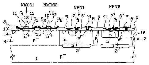
Fig. 1 shows a cross-section of a BiCMOS circuit, including
two types of transistors manufactured according to the
invention.
CA 02349559 2001-04-30
WO 00/26962 PCT/SE99/Ot 942
6
Fig. 2a-2c shows cross-sections of different manufacturing
steps for two NPN bipolar transistors having different
characteristics according to the invention.
Fig. 3a-3e shows cross-sections of different manufacturing
steps for two NMOS transistors having different
characteristics according to the invention. w
Detailed Description of Embodiments
Fig. 1 shows a cross-section of a BiCMOS circuit, including
two types of transistors manufactured according to the
invention. The BiCMOS circuit is manufactured on a substrate 1
being doped with a dopant of a first type, in this example p.
Buried layers 2 are arranged between the substrate and an
epitaxial layer 3. Each buried layer 2 is doped with a dopant
of a second type, in this example n, and forms a part of a
collector in a bipolar transistor NPN1 and NPN2, which is a
first type of transistor.
The epitaxial layer 3 is initially doped with a dopant of the
first type p, and a second type of transistor, NMOS transistor
NMOS1 and NMOS2, is implemented in this region, the so called
MOS-region 4. The region above the buried layers 2 is doped
with a dopant of the second type n, to form a bipolar region
16 (BIP-region), where the bipolar transistors are
implemented.
The MOS-region 4 is in this case the epitaxial layer 3, but
may be any suitable doped well, p or n type. The epitaxial
layer 3 is, for clarity reasons, regarded to be a well of said
first type p.
Each bipolar transistor needs to be fully isolated from
neighbouring devices. This is achieved by implementing
CA 02349559 2001-04-30
WO 00/26962 PCT/SE99/01942
7
isolation regions 5, extending from the substrate 1 up to the
surface of the epitaxial layer 3. Each bipolar transistor have
a base region 6', f", being doped with a dopant of the first
type p, and within that base region an emitter region 7, being
doped with a dopant of the second type n. A collector region
8, being doped with a dopant of the second type n, is
implemented beside the base region 6', 6". Each bipolar
transistor NPN1, NPN2 then have an emitter contact el, e2, a
base contact bl, b2 and a collector contact cl, c2.
Each NMOS transistors have a channel region 10', 10", being
doped with a dopant of the same type as the MOS-region (p). A
gate oxide 11 a polysilicon gate 12 and spacers 13 are then
created on top of each channel region 10', 10". A source
region 14 and a drain region 15 are implemented, in the MOS-
region 4, on each side of the gate 12.
The inventive method for manufacturing transistors is
applicable for various types of active devices, such as
bipolar transistors and MOS-transistors, as is described
below. Other types of active devices may also be manufactured
by the inventive method. The common methods for manufacturing
semiconductor devices are not described in details, since they
are obvious to a person skilled in the art, and the inventive
method is described as a complement to those methods.
Fig. 2a-2d shows partial cross-sections of a semiconductor
circuit during different manufacturing steps for the two NPN
bipolar transistors, from Fig. 1, having different
characteristics according to the invention.
Fig. 2a shows a cross-section of a substrate (partially shown)
having buried layers 2 and epitaxial layer 3, where said
epitaxial layer have been doped with a dopant of the second
CA 02349559 2001-04-30
WO 00/26962 PCT1SE99/OI942
8
type n to form a BIP-region 16. Isolation regions 5 have been
implemented to isolate the bipolar transistors from each
other. During these process steps, a layer of field oxide 20 '
have been created on top of the BIP-region 16. A first dopant
P1 of a first type p, e.g. Boron, is ion implanted through a
first and second opening 21, 22 in the oxide layer 20. Said
first dopant having a first set of dose parameters, e.g.
energy and implantation time, which results in a number of
impurities 23, at a first depth, in the BIP-region 16. These
impurities are marked as plus signs in the drawing to indicate
that the present impurity creates a shortage of electrons
(group III elements).
Fig. 2b shows a cross-section of same devices as Fig. 2a with
the addition of a protective layer 24, e.g. photo resist,
covering said first opening 21. A second dopant P2, of the same
type as the first dopant, is thus only implanted through said
second opening 22. Said second dopant P2 having a second set of
dose parameters, which result in another number of impurities
25, at a second depth, in the BIP-region 16. Thus creating a
combination of said first and second set of parameters.
The relationship between said first and second depth may be
arbitrary, and even identical. The important difference
between said the ion implantation through said first and
second opening is that at Least one parameter of said first
set of dose parameters and the combination of said first and
second set of parameters is different, e.g. if the same
impurity is used, a difference in ion implantation energy
results in additional impurities at an additional depth and a
difference in ion implantation time, using the same impurity,
results in different number of impurities at the same depth.
CA 02349559 2001-04-30
WO 00/26962 PCT/SE99/01942
9
The protective layer is removed and the device is subject to
an annealing step for a predetermined time to distribute the
impurities and form base regions 6', 6". The base regions
having different doping profiles due to the previous
implantation steps. During the annealing step, a base oxide 26
is grown on top of each base region. This is illustrated in
Fig. 2c.
An emitter region 7 is formed in the base region 6', 6" and a
collector region 8 is formed on the side of said base region.
At the same time an emitter oxide 27 and a collector oxide 28
is grown on top of each region, respectively. An illustration
of this is shown in Fig. 2d.
The emitter.region, base region and collector region are then
contacted to establish an emitter contact el, e2, a base
contact bl, b2 and a collector contact cl, c2, as is shown in
Fig. 1. This makes it possible to interconnect the
semiconductor devices on a semiconductor circuit or directly
access the transistors.
This technique for manufacturing bipolar transistor with
different doping profiles in the base region, may of course be
used for manufacturing bipolar transistor with different
collector or emitter regions. Different doping profiles in the
collector region provides devices that could work with
different supply voltages or different frequency
characteristics, according to "Johnson Limit", on the same
integrated circuit, and different doping profiles in the
emitter regions causes more or less the same effect as
variation of the doping profiles in the base regions.
CA 02349559 2001-04-30
WO 00/26962 PCT/SE99/01942
Fig. 3a-3e shows cross-sections of a semiconductor circuit
during different manufacturing steps for two NMOS transistors
having different characteristics according to the invention.
Fig. 3a shows a cross-section of an epitaxial layer 3 being
5 grown on top of the substrate (not shown). The epitaxial layer
forms a MOS-region 4, which is doped with a dopant of the
first type p, as described above. During previous process
steps, a field oxide 30 has been created on top of the MOS-
region 4. A first 31 and a second 32 opening are arranged in
10 the field oxide 30, and instead of implanting both exposed
areas of the MOS-region 9, a first protective coating 33 is
placed over one of the openings, in this example the second
opening 32. A first dopant P3 of the second type p is
introduced through said first opening 31 by means of ion
implantation, which results in a number of impurities 34 in
said exposed MOS-region.
It is of course possible to implant the first impurity through
both openings as in the previous example, but this example
illustrates the possibility to make arbitrary combinations.
The first protective coating 33 is then removed and a second
protective coating 35 is placed over said first opening 31,
exposing said MOS-region 4 through second opening 32, as shown
in Fig. 3b. A second dopant P9 of the second type p is
introduced through said second opening 32 by means of ion
implantation, which results in another number of impurities 36
in said exposed MOS-region.
The protective coating is removed and a gate oxide 11 is then
deposited on top of said exposed MOS-regions. The device is
subject to an annealing step during manufacture of said gate
oxide 11 and the impurities are distributed to form doped
CA 02349559 2001-04-30
WO 00/26962 PCT/SE99/01942
11
regions 37', 37". The result of these steps is shown in Fig.
3c.
Fig. 3d shows a cross-section of the device from Fig. 3c,
where a polysilicon gate 12 have been created with spacers 13.
These manufacturing steps are familiar to a person skilled in
the art, and so is the manufacturing steps describing the''
manufacture of source 14 and drain 15 regions and doping of
the polysilicon gate 12 by utilising ion implantation with a
dopant N1 of the second type n, such as Arsenic, as is
described in Fig. 3e. The establishment of source and drain
region distributes the impurities further in the doped regions
37', 37" and also reduces the doped regions into channel
regions 10', 10", where said channel regions have different
doping profiles and different threshold voltage.
These examples only show two transistors of each type, but it
is to be understood that an arbitrary number of transistor
within each type may be implemented using the inventive
method. Furthermore, the method is not limited to just two
types of transitors, but may be used for any number of
transistor types.
The shown examples only show bipolar NPN and NMOS transistors,
but the method may readily be used when manufacturing bipolar
PNP and PMOS transistors, or any other type of transistor,
such as double poly bipolar transistors for high frequencies.
The protective coating is preferable made of a photo resist,
due to the non-destructible removal process, but other
coatings may be used, such as oxide, nitride and polyimide.