Note: Descriptions are shown in the official language in which they were submitted.
CA 02349636 2001-05-04
WO 00/28613 PCTNS99/26113
FERROELECTRIC VARACTOR WITH BUILT-IN DC BLOCKS
CROSS REFERENCE TO RELATED PATENT APPLICATION
This application claims the benefit of United States Provisional Patent
Application No. 60/ 107,684, filed November 9, 1998.
FIELD OF INVENTION
The present invention relates generally to voltage tunable varactors
with associated DC blocking capacitors.
BACKGROUND OF INVENTION
Varactors are voltage tunable capacitors in which the capacitance is
dependent on a voltage applied thereto. This property can find applications in
electrically tuning radio frequency (RF) circuits, such as filters, phase
shifters, and so
on. The most commonly used varactor is semiconductor diode varactor, which has
the advantages of high tunability and low tuning voltage, but suffers low Q,
low
power handling capability, and limited capacitance range. A new type of
varactor is a
ferroelectric varactor in which the capacitance is tuned by varying the
dielectric
constant of a ferroelectric material by changing the bias voltage.
Ferroelectric
varactors have high Q, high power handling capacity, and high capacitance
range.
One ferroelectric varactor is disclosed in United States Patent No.
5,640,042 entitled "Thin Film Ferroelectric Varactor" by Thomas E. Koscica et
al.
That patent discloses a planar ferroelectric varactor, which includes a
carrier substrate
layer, a high temperature superconducting metallic layer deposited on the
substrate, a
lattice matching, a thin film ferroelectric layer deposited on the metallic
layer, and a
plurality of metallic conductors disposed on the ferroelectric layer and in
contact with
radio frequency (RF) transmission lines in tuning devices. Another tunable
capacitor
using a ferroelectric element in combination with a superconducting element is
CA 02349636 2001-05-04
WO 00/28613 PCT/US99/26113
2
disclosed in United States Patent No. 5,721,194. Tunable varactors that
utilizes a
ferroelectric layer, and various devices that include such varactors are also
disclosed
in United States Patent Application Serial No. , entitled "Voltage Tunable
Varactors And Tunable Devices Including Such Varactors ", filed October 15,
1999,
and assigned to the same assignee as the present invention.
When using such varactors in various devices, it is necessary to insert
DC blocking capacitors in the RF transmission line to isolate the DC bias
voltage
from the other parts of RF system. These DC blocks on the transmission line
may
result in additional insertion loss to the RF system, and inconvenience in the
design
and construction of an RF system.
There is a need for varactors with reduced DC block insertion loss, but
with high tunability, for use in the VHF, UHF, microwave and other tunable
circuits,
such as filters, phase shifters, voltage controlled oscillators and so on.
SUMMARY OF INVENTION
A voltage tunable dielectric varactor assembly constructed in
accordance with this invention includes a tunable ferroelectric layer and
first and
second non-tunable dielectric layers. First and second electrodes positioned
adjacent
to the tunable ferroelectric layer form a tunable capacitor. The first and
second
electrodes are also positioned adjacent to the first and second non-tunable
layers,
respectively. A third electrode is positioned adjacent to the first non-
tunable
dielectric layer such that the third and first electrodes and the first non-
tunable
dielectric layer form a first blocking capacitor. A fourth electrode is
positioned
adjacent to the second non-tunable dielectric layer such that the fourth and
second
electrodes and the second non-tunable dielectric layer form a second blocking
capacitor.
In one embodiment, the voltage tunable dielectric varactor includes a
substrate having a generally planar surface and a tunable ferroelectric layer
positioned
on the generally planar surface of the substrate. First and second electrodes
are
positioned on a surface of the tunable ferroelectric layer opposite the
generally planar
surface of the substrate, with the first and second electrodes being separated
to form a
first gap. First and second non-tunable dielectric layers are also positioned
on the
generally planar surface of the substrate. A third electrode is positioned on
the
CA 02349636 2001-05-04
WO 00/28613 PCTNS99/26113
3
surface of the first non-tunable dielectric layer opposite the generally
planar surface of
the substrate such that the third and first electrodes form a second gap. A
fourth
electrode is positioned on the surface of the second non-tunable dielectric
layer
opposite the generally planar surface of the substrate such that the fourth
and second
electrodes form a third gap.
In another embodiment, the voltage tunable dielectric varactor includes
a tunable ferroelectric layer and first and second non-tunable dielectric
layers. The
tunable layer is positioned between first and second electrodes to form a
tunable
capacitor. The first non-tunable layer is positioned between the first
electrode and a
third electrode to form a first blocking capacitor. The second non-tunable
layer is
positioned between the second electrode and a fourth electrode to form a
second
blocking capacitor.
Ferroelectric varactor assemblies of the present invention can be used
to produce a phase shift in various microwave devices, and in other devices
such as
tunable filters.
BRIEF DESCRIPTION OF THE DRAWINGS
A full understanding of the invention can be gained from the following
description of the preferred embodiments when read in conjunction with the
accompanying drawings in which:
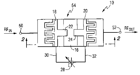
FIG. 1 is a top view of a planar varactor assembly with built-in DC
blocking capacitors constructed in accordance with the invention;
FIG. 2 is a cross sectional view of the varactor assembly of FIG. 1,
taken along line 2-2;
FIG. 3 is an equivalent circuit of the varactor with built-in DC block
capacitors of FIGs. 1 and 2;
FIG. 4 is a graph of the tunability versus capacitance ratio for a
varactor assembly constructed in accordance with the invention
FIG. 5 is a top view of a varactor assembly with built-in DC blocking
capacitors constructed in accordance with another embodiment of the invention;
FIG. 6 is a cross sectional view of the varactor assembly of FIG. 5,
taken along line 6-6;
CA 02349636 2001-05-04
WO 00/28613 PCTNS99/Z6113
4
FIG. 7 is a top view of a varactor assembly with built-in DC blocking
capacitors constructed in accordance with another embodiment of the invention;
and
FIG. 8 is a cross sectional view of the varactor assembly of FIG. 7,
taken along line 8-8.
S DETAILED DESCRIPTION OF THE PREFERRED EMBODIMENTS
Referring to the drawings, FIGS. 1 and 2 are top and cross sectional
views of a varactor assembly 10 constructed in accordance with this
invention.. The
varactor assembly 10 includes a substrate 12 having a generally planar top
surface 14.
A tunable ferroelectric layer 16 is positioned adjacent to the top surface of
the
substrate. Metal electrodes 18 and 20 are positioned on top of the
ferroelectric layer.
The electrodes 18 and 20 are shaped to have projections 22 and 24. The ends of
these
projections form a gap 26 on the surface of the tunable ferroelectric layer.
The
combination of electrodes 18 and 20, and tunable ferroelectric layer 16 form a
tunable
capacitor 54. The capacitance of the tunable capacitor can be changed by
applying a
bias voltage to the electrodes 18 and 20.
In the preferred embodiment, the substrate 12 is comprised of a
material having a relatively low permittivity such as MgO, Alumina, LaAl03,
Sapphire, or a ceramic. For the purposes of this invention, a low permittivity
is a
permittivity of less than about 30. In the preferred embodiment, the tunable
ferroelectric layer 16 is comprised of a material having a permittivity in a
range from
about 20 to about 2000, and having a tunability in the range from about 10% to
about
80% at a bias voltage of about 10 V/pm. The tunable ferroelectric layer can be
comprised of Barium-Strontium Titanate, BaXSri.XTi03 (BSTO), where x can range
from zero to one, or BSTO-composite ceramics. Examples of such BSTO composites
include, but are not limited to: BSTO-MgO, BSTO-MgA1204, BSTO-CaTi03, BSTO-
MgTi03, BSTO-MgSrZrTi06, and combinations thereof. The dielectric film of the
ferroelectric capacitor may be deposited by screen printer, laser ablation,
metal-
organic solution deposition, sputtering, or chemical vapor deposition
techniques. The
tunable layer in one preferred embodiment has a dielectric permittivity
greater than
100 when subjected to typical DC bias voltages, for example, voltages ranging
from
about 5 volts to about 300 volts. The gap width must be optimized to increase
ratio of
the maximum capacitance Cm~ t0 the minimum capacitance Cm;n (Cm~/Cmin ) ~d
CA 02349636 2001-05-04
WO 00/28613 PCT/US99/26113
increase the quality facto (Q) of the device. The width of this gap has the
most
influence on the varactor parameters. The optimal width, g, will be determined
by the
width at which the device has maximum Cm~/Cm;" and minimal loss tangent.
A controllable voltage source 28 is connected by lines 30 and 32 to
5 electrodes 18 and 20. This voltage source is used to supply a DC bias
voltage to the
ferroelectric layer, thereby controlling the permittivity of the layer. The
varactor
assembly further includes first and second non-tunable dielectric layers 34
and 36
positioned adjacent to the generally planar surface of the substrate 12 and on
opposite
sides of the tunable ferroelectric layer 16. Electrode 18 extends over a
portion of the
top surface of non-tunable material 34. Electrode 38 is positioned adjacent a
top
surface of non-tunable layer 34 such that a gap 40 is formed between
electrodes 18
and 34. The combination of electrodes 18 and 34 and non-tunable layer 34 forms
a
first DC blocking capacitor 42. The varactor assembly also includes an RF
input 30
and an RF output 32.
Electrode 44 is positioned adjacent a top surface of non-tunable layer
36 such that a gap 46 is formed between electrodes 20 and 44. The combination
of
electrodes 20 and 44 and non-tunable layer 36 forms a second DC blocking
capacitor
48. The dielectric films of the DC blocking capacitors may be deposited by
screen
printer, laser ablation, metal-organic solution deposition, sputtering, or
chemical
vapor deposition techniques.
An RF input 50 is connected to electrode 38. An IZF output 52 is
connected to electrode 44. The RF input and output are connected to,
electrodes 38
and 44, respectively, by soldered or bonded connections. The non-tunable
dielectric
layers 34 and 36, in the DC blocking capacitors 42 and 48, are comprised of a
high
dielectric constant material, such as BSTO composite. The DC blocking
capacitors 42
and 48 are electrically connected in series with the tunable capacitor 54 to
isolate the
DC bias from the outside of the varactor assembly 10. To increase the
capacitance of
the two DC blocking capacitors 42 and 48 the electrodes have an interdigital
arrangement as shown in FIG. 1.
In the preferred embodiments, the varactors may use gap widths of 5-
50 pm. The thickness of the ferroelectric layer ranges from about 0.1 pm to
about 20
l,un. A sealant can be inserted into the gaps to increase breakdown voltage.
The
CA 02349636 2001-05-04
WO 00/28613 PCT/US99/26113
6
sealant can be any non-conducting material with a high dielectric breakdown
strength
to allow the application of high voltage without arcing across the gap, for
example,
epoxy or polyurethane.
The equivalent circuit of the varactor assemblies of this invention is
shown in FIG. 3. The circuit is comprised of a tunable capacitor CI connected
in
series to two non-tunable DC block capacitors C2 have equal capacitance in
this
example. Therefore, the resultant capacitor Ct of the varactor assembly is
expressed as
_1 _ 1 + 2 (1)
Cr CI Cz
or,
Cr = 1 2
C, 1 + 2C, ( )
CZ
Here C1 is the capacitance of tunable capacitor, and C2 is the capacitance of
DC
block capacitors. In the case of:
C, « Cz (3)
Equation (2) gives:
C, ~ C,
the tunability of resultant capacitor is related to that of the capacitor
C,. The tunability, t, of material can be defined as
t~e dE ( )
r
where sr is the dielectric constant of the material, and E is strength of
applied field. In
the case of a capacitor where tunable material is used, often the capacitance
C of the
capacitor varies linearly with the dielectric constant, that is:
C = aE, (6)
where a is a capacitor parameter constant related to the geometrical
structure, such as
area, thickness and so on. The tunability can then be expressed as:
t = 1 dE, ' 1 dC (
s, dE C dE
CA 02349636 2001-05-04
WO 00/28613 PCT/US99/26113
7
If C, is a tunable capacitor with tenability t, and C2 is a non-tunable
capacitor, the resultant tenability t, of the varactor assembly can be
obtained from
Equation ( 1 ) and Equation (7)
t-'' t-'' (g)
C, C,
Using Equation (2), Equation (8) can be rewritten so that:
_t, _ C, _ 1
t' C' 1 + 2C' (9)
C2
here tt is the resultant tenability of the varactor assembly. Equation (1)
shows that:
C, < C, ( 10)
since both C, and C2 are both positive numbers. Therefore, from Equation (9),
t, < t, ( 11 )
If the condition of Equation (3) is applied ( C, « CZ ),
tr ~ ti
(12)
FIG. 4 shows the relationship of Equation (9) graphically. For example, it can
be seen
that at:
~-2 = 20 , we have t-'' = C' = 0.91.
C, t, C,
and at CZ = 40 , we have t-'' = C' = 0.95 .
C~ t~ C~
Therefore, if CZ»C,, the resultant capacitance C, and tenability t~ are
mostly determined by the tunable capacitor C,. Very little additional
insertion loss is
incurred through the integration of the DC blocking capacitors in the present
invention, since the capacitance of the DC blocking capacitors is much higher
than the
capacitance of the varactor portion of the assembly. The insertion loss of the
varactor
assembly of the present invention results primarily from the tunable
ferroelectric
capacitor and its connections, since the capacitance of the tunable
ferroelectric
capacitor is much smaller than that of DC blocking capacitors.
FIGS. 5 and 6 are top and cross sectional views of a varactor assembly
56 with planar capacitor structure. In FIGs. 5 and 6, a capacitor 58 is a
tunable
CA 02349636 2001-05-04
WO 00/28613 PCTNS99/26113
8
parallel-plate capacitor with DC bias metallic layer electrodes 60 and 62,
which have
bias terminations 64 and 66, respectively. The tunable material 68 in the
capacitor 58
may be BSTO-based or related materials in the styles of bulk, tape, or thin
film. DC
block capacitors 70 and 72 are parallel-plate capacitors, which are connected
in series
to the tunable capacitor 58, respectively. The dielectric material 74 and 76
used in
capacitors 70 and 72 is non-tunable material with high dielectric constant in
the styles
of bulk, tape or film. The capacitance of the DC blocking capacitors 70 and 72
should
be at least 20 times higher than that of the tunable capacitor 58 by properly
selection
of dielectric constant of the dielectric material and the thickness of the
dielectric
layers. Electrodes 78 and 80 of the varactor assembly 56 are connected to a
radio
frequency (RF) signal though terminals 82 and 84. In order to satisfy the
condition of
C2»C1 in Equation (3), higher dielectric constant and thinner non-tunable
layers 74
and 76, compared to the tunable layer 68, are chosen for the DC blocking
capacitors
70 and 72 to increase the capacitance.
1 S FIGS. 7 and 8 show a third embodiment of a varactor assembly 86
constructed in accordance with the present invention. The structure of
varactor
assembly 86 is similar to that of varactor assembly 56. However, multilayer
capacitors are used as the DC blocking capacitors in varactor assembly 86 to
replace
the single layer DC blocking capacitors in varactor assembly 56 to increase
the
capacitance. The dielectric materials in this structure may be tape, thin or
thick films.
In FIGs. 7 and 8, a capacitor 88 is a tunable capacitor with DC bias metallic
layer
electrodes 90 and 92, which have bias terminations 94 and 96, respectively.
The
tunable material 98 in the capacitor 88 may be BSTO- based or related
materials. The
multilayer DC blocking capacitors 100 and 102 are connected in series to the
tunable
capacitor 88, respectively. The dielectric material used in capacitors 100 and
102 is
non-tunable material with a high dielectric constant. With this embodiment, he
capacitance of the DC blocking capacitor 100 and 102 should be at least 40
times
higher than that of the tunable capacitor 88 by proper selection of the
dielectric
material, the thickness of the dielectric layer, and the number of dielectric
layers.
Electrodes 104 and 106 of the varactor assembly 86 are connected to the RF
transmission lines through the electrode terminations 108 and 110.
CA 02349636 2001-05-04
WO 00/28613 PCTNS99/26113
9
A ferroelectric varactor assembly with built-in DC blocks) has been
described, in which low loss and high tunability materials are used. The built-
in DC
blocking capacitors make the varactor much easier to use in RF circuits, and
eliminate
the insertion loss caused by conventional DC blocking capacitors when
conventional
varactor is used. The low loss and high tunability materials may be Barium-
strontium
titanate, BaxSrl-xTi03 (BSTO), where x is less than 1, or BSTO- based
composites.
These high quality materials may significantly improve the varactor
performance of
the present invention. The ferroelectric varactor may be made of bulk, thin
film, or
thick film ferroelectric materials.
Accordingly, the present invention, by utilizing built-in DC blocking
capacitors and high quality tunable ferroelectric materials, provides a high
performance of ferroelectric varactor assembly, elimination of conventional DC
block
insertion loss, and significant convenience for RF circuit design and
processing. This
invention has many practical applications and many other modifications of the
disclosed devices may be obvious to those skilled in the art without departing
from
the spirit and scope of this invention as defined by the following claims.