Note: Descriptions are shown in the official language in which they were submitted.
CA 02349647 2001-05-31
~ACKOROUND OF THE INVENTI-ON
(1) Field of the Invention
The present invention relates to an image display apparatus by a projector
for displaying images by projection through single polarizer, the display
apparatus being primarily designed for the improvement of the contrast.
(2) Description of the Prior Art
Recently, the projectors have been evolving for further compactness and
lightweight as is obvious from that many manufactures are active for the
development of the mobile projectors. However, in development such
compact and lightweight mobile projectors, it is essential to provide a highly
efficient optical system in order to ensure thf; normal levels for both the
luminance and contrast (e.g. 1000 ANS for luminance and 400:1 for contrast).
However, in order for the luminance to be kept at an necessary level, it is
necessary to raise the light quantity or the power of the light source lamp,
but
raising the light quantity or the power of the light source lamp gives rise to
a
problem, i.e., the increase in the leak of the light that results in an
adverse
effect on the contrast.
The detail of a conventional projector will be described referring to Figs.
and 11.
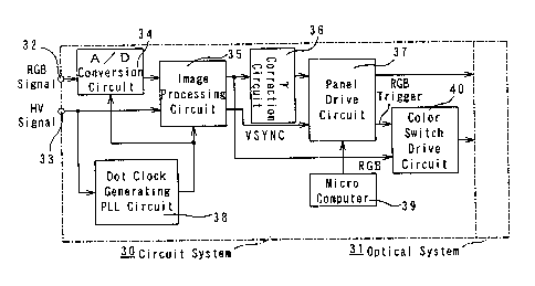
In the case shown in Fig. 10, the projector comprises a circuit system 10 and
an optical system 11. In the circuit system :LO, AID conversion circuit 14
serves for converting analog R, G and B video signals inputted to RGB video
signal input terminal 12 to digital R, G and B signals. Dot clock generating
PLL circuit 18 generates the dot clock on the basis of HSYNC (Horizontal
1
CA 02349647 2001-05-31
Synchronizing Signal) inputted to HV synchronising signal input terminal 13
from the outside of the display apparatus. Image processing circuit 15 is
designed for processing the digital R, G and B signals, which have been
converted by the A/D conversion circuit 14, for scaling and for obtaining a
resolution suiting to display panel 26 of the optical system 11. y correction
circuit 16 is designed for correcting the inputted image data to the colors
suiting to the display panel. Panel drive circuit 17 is for driving the
display
panel 26. Color switch drive circuit 20 is provided for driving the filters
(color switch) for coloring the picture elements displayed at the tone levels
of
the R, G and B signals according to the commands given from a microcomputer
19.
In the optical system 11, light source unit 21 includes a light source lamp,
an integrator lens, a polarizing conversion element, a condenser lens or the
like.
Polarizes 22 is designed for removing P wave component (optical component
oscillating parallel to incident plane) of the light from the light source,
leaving
only S wave component (optical component oscillating vertically to incident
plane).
The color switch 23 is designed to turn the direction of polarization of one
of R, G and B. The color switch 23 comprises 3 pieces of transmission liquid
crystal panels corresponding to R, G and B <;olors and a retardation film
capable of turning only the polarized light of a specific wavelength band,
which
are put together in an accumulated form. With. this color switch 23, when an
R light is necessary, only the polarized light of the wavelength band of the R
light is turned into P wave while keeping the wavelength bands of the G and B
lights unturned to maintain S wave components thereof, whereby the polarized
G and B lights are reflected by the polarization beam splitter prism 24
(hereinafter referred to as PBS) while only the polarized R light is permitted
to
pass through and to reach the reflection display panel 26. Of the light with
the P wave component that has arrived at the reflection display panel, only
the
2
CA 02349647 2001-05-31
picture element to be displayed is turned into S wave to be reflected
according
the video information. Of the light reflected by the reflection display panel
26, only the S wave component is reflected in a direction at 90° to the
PBS 24
to be finally projected on the screen. When either the G light or the B light
is necessary, it is also possible to turn the wavelLength band of either light
by
means of the color switch 23.
The sticking owing to the memory effect is apt to occur with the reflection
display panel because of the characteristic of the liquid crystal panel,
unless
the polarity of the voltage is changed. Therefore, the doubles 25 consisting
of a polarizing switching element for correction for preventing the reversing
of
the black color or white color, which is apt t~o occur when the polarity is
changed from positive to negative or vice versa, is provided before the
reflection display panel 26.
The control timing of the color switch drive; circuit 20 in a conventional
display apparatus will be explained below referring to Fig. 11.
The VSYNC (a) is a frame synchronizing signal to be externally inputted to
HV synchronizing signal input terminal 13 and then inputted to the color
switch
drive circuit 20 through the image processing circuit 15, and the display is
made according to this synchronizing signal. ~~s for the timing of the display
on the panel (b), in the case of the single polarizes display unit with a
projector,
the color tones for the display by R, G and B lights have to be set in order
within the display period for 1 frame. The timing of switching corresponds
to the display on the panel (b). The color switch trigger (c) is a signal
synchronized with the VSYNC and is inputted so as to be capable of switching
the color switch 23, synchronizing with the switching of the drive of the
panel.
Color switch signal (d) represents the timing for the switching of the color
switch 23, and it is best for the color switch 23 of the R, G and B colors to
be
switched synchronizing with the color tone displlay of the R, G and B lights.
However, since the color switch trigger signal to be inputted is only one
3
CA 02349647 2001-05-31
synchronized with the VSYNC, when the operatiion of the color switch 23 is
varied for the purpose such as the adjustment of the white balance, this is
apt to
give rise to a problem that some timing lag occurs with respect to the color
tone
display for the drive of the panel as is represented by the sections marked
with
slant lines of the color switch (d), causing the deterioration of the
contrast.
Since mere sequential repetition of the R, G and B display spoils the purity
of the white color entailing the fall of the luminance, it has come to be
considered to include the white in the switching cycle of the R, G and B
colors.
Simply inserting the white color, however, makes the color tone of the whole
image whitish, bringing about unnatural blackening and poor contrast of the
image.
The present invention is made in order to resolved the problems of the prior
art described above. The first object of the present invention is to provide a
display apparatus by a projector, wherein both the luminance and the contrast
of the displayed image are improved by inserting the white color or black
color
among the displayed color tones of the picture element corresponding to the R,
G and B colors for a predetermined period of time by means of the color switch
without entirely relying on the light quantity or the power of the light
source
lamp; in order to improve the luminance and the contrast, the mean luminance
of the picture element to be displayed is calculated so that the white color
or
the black color is selectively inserted on the basis of the mean luminance,
and
the time period of the insertion is varied according to the sampled mean
luminance.
In the method in which the light is separated into R, G and B components to
be displayed sequentially within a frame, a phenomenon called the false
contouring will occur commonly. The false contouring is caused by the
luminance difference occurring when the display of an image of, for example, R
4
CA 02349647 2001-05-31
color corresponding to a high luminance information is followed by the display
of an image of, for example, G color corresiponding to a relatively low
luminance, since such luminance difference causes the formation of the after
image that accentuates the contour of the R color, Such a problem, however,
can be reduced by suppressing the luminance difference to a largest possible
extent.
The second object of the present invention is to alleviate the false
contouring by detecting the mean luminance of the image so that when the
image is relatively dark, the black color is inserted while inserting the
white
color when the image is relatively bright, and the false contouring is
alleviated
by reducing the difference in luminance among the cells through controlling
the
time period of the insertion.
Further, the present invention enables the timing signals for actually
displaying the color tones for the R, G and B colors to be outputted
separately
by the panel drive circuit, the white balance to be adjusted by adjusting the
timing signal, and the timing of the color tone display and that of color
switch
operation to be synchronized with each other for the improvement of the
contrast.
The present invention relates to a single polarizer projector, of an image
display apparatus, comprising a image processing circuit for the scaling
process of the image, a y correction circuit for correcting the y for
obtaining a
proper color suiting to the display panel, a color switch for assigning the
color
for the color tone display by the display panel and a color switch drive
circuit
for driving the color switch, wherein the color switch drive circuit
determines
the mean luminance of the picture element data (original image) of the image
processing circuit so that the white color or blank color can be inserted
among
the displayed color tones corresponding to the R, G and B colors on the basis
of
the value of the mean luminance, thereby expanding the dynamic range of image
display.
CA 02349647 2001-05-31
The triggers for driving the color switch constitute the triggers for the R, G
and B colors, and the triggers, when inputted to the color switch drive
circuit,
enable the display of the color tones by the panel and the coloring by the
color
switch to be synchronized with each other for being accomplished.
The image display apparatus by a projector according to the present
invention is characterized by that the basis of selection of either the white
or
black is set to the mean luminance of 50% so that the white is inserted when
the
mean luminance is 50% or more while the black is inserted when the mean
luminance is less than 50% to expand the dynamic; range for the improvement of
the contrast.
Further, the image display apparatus by a projector may be characterized by
that the timing for inserting the white color or the black color is controlled
according to the mean luminance so that the purity of the white color or the
black color can be raised while maintaining the purities of other factors.
Further, the image display apparatus by a :projector may be designed to
comprise the color switch drive circuit, which includes an RGB/Y conversion
circuit for converting the R, G and B into the luminance signal respectively,
the
mean luminance calculation circuit for determining the mean luminance, a
white color or black color insertion timing control circuit for setting the
timing
for the insertion of the white color or black color, and the D/A conversion
circuit, so that the triggers corresponding to the R, G and B colors are
inputted
to the white color/black color insertion timing control circuit, whereby the
white color/black color insertion timing control circuit synchronizes the
first
half of the trigger with each of the triggers to output the color information
corresponding to each of the triggers, while outputting the white or black
information according to the mean luminance and corresponding to the latter
half of the trigger.
Further, the image display apparatus by a projector may be designed to
comprise the color switch drive circuit, which includes the RGB/Y conversion
6
CA 02349647 2001-05-31
circuit for converting the R, G and B into the luminance signals, the mean
luminance calculation circuit for determining the mean luminance, the white
color or black color insertion timing control circuit for generating the
timing
signal for the insertion of the white color or black color, and the D/A
conversion circuit for converting the output of the white color or black color
insertion timing control circuit into analog signal, so that a trigger is
inputted
to the white color or black color insertion timing control circuit to generate
the
output timing signal corresponding to each of the R, G and B colors, whereby
the color information corresponding to the generated output timing signal is
outputted, and the white color or black color information is outputted
corresponding to the man luminance corresponding to the latter half of the
trigger.
Further, the image display apparatus by a projector may be designed so that,
in outputting the color information according to the trigger, the voltage of
the
output from the D/A converter is controlled according to the mean luminance to
control the transmittance of the color switch and to thereby improve the
contrast.
Further, the image display apparatus by a projector may comprise the white
color and black color insertion timing control ciircuit including a first
counter
for counting the pulse width of the trigger signal, a second counter for
detecting by counting the assert position of the trigger signal, a ratio
calculator
for varying the pulse width counted by the first counter according to the mean
luminance, a W/B selector for selecting either white color or black color to
be
inserted according to the mean luminance, a pulse generator for asserting the
pulse width calculated by the ratio calculator at the timing counted by the
second counter, and an output controller for selecting the color information
corresponding to the timing trigger signal generated by the pulse generator or
the white color or black color information which has been selected by the W/B
selector, thereby enabling the white or black color information to be inserted
7
CA 02349647 2001-05-31
for the improvement of the contrast.
Further, the image display apparatus by a projector may comprise a register
for enabling the assert position to be set freely and a register for enabling
the
negate position to be set freely so that each trigger signal can be generated
by
counting the clock which is shifted towards the vertical synchronizing signal
by
the value of the freely settable register, thereby f;nabling each trigger
signal to
be generated.
Further, the image display apparatus by a projector may be designed so that
RGB trigger generator comprises the register capable of freely setting the
assert position and the register for freely setaing the active pulse width,
whereby the trigger is asserted by counting the clock, which is shifted
towards
the vertical synchronizing signal by the value of the freely settable
register,
and the trigger signal is negated by counting the clock by the number of the
clock of the pulse width register, on the basis of the trigger assert
position.
Further, the image display apparatus by using a projector may be designed
so that, in outputting the color information corresponding to the trigger, the
improvement of the contrast is sought by controlling the insertion timing of
the
white or black color while controlling the voiLtage outputted from the D/A
conversion circuit according to the mean luminance, and that other purities
can
be maintained while raising the purity of the white color or the black color.
Fig. 1 is a block diagram of a image display apparatus by a projector as an
embodiment of the present invention.
Fig. 2 is a block diagram showing the detail of the color switch drive circuit
given in Fig. 1.
Fig. 3 is a block diagram showing the detail of another example of the color
switch drive circuit given in Fig. 1.
Fig. 4 is a waveform diagram of the timing signal of the projector according
8
CA 02349647 2001-05-31
to the present invention.
Fig. 5 is a block diagram showing the detail of the white color and black
color insertion timing control circuit given in Fig. 2 and Fig. 3.
Fig. 6 is a waveform diagram of the timing signal from the white color and
black color insertion timing control circuit given in Fig. 5.
Fig. 7 is a block diagram of the circuit for outputting three independent
trigger signals, i.e., those corresponding to the R, G and B colors, from the
panel drive circuit 37 to the white color and black color insertion timing
control circuit 43 within the color switch drive circuit 40.
Fig. 8 is a block diagram of a trigger generating means 62 for generating R
trigger, G trigger and B trigger according to 1 trigger and dot clock from the
panel drive circuit 37.
Fig. 9 is a block diagram showing an example of the R trigger generating
means 62R among the RGB trigger generating means 62 given in Fig. 8.
Fig. 10 is a block diagram of a conventional image display apparatus by a
projector.
Fig. 11 is a timing signal waveform diagram of a conventional image
display apparatus by a projector given in Fig. 1Q.
The embodiments of the present invention will be explained below referring
to pertinent drawings.
In Fig. 1, the A/D conversion circuit 34, the image processing circuit 34,
the y correction circuit 36 and the dot clock ;;enerating PLL circuit 38 are
similar to the A/D conversion circuit 14, the image processing circuit 15, the
y
correction circuit 16 and the dot clock generating PLL circuit 18 of the
conventional circuit system 10 given in Fig. 10.
The panel drive circuit 37 has the function to generate the signals
representing the tones of the R, G and B colors respectively and the trigger
9
CA 02349647 2001-05-31
signals corresponding to the R, G and B colors synchronized with the signals
representing the tones of the R, G and B colors. The trigger signals
corresponding to the R, G and B colors respectively can readily be generated
by
the panel drive circuit, on the basis of the start sii;nals representing the
tones of
the R, G and B colors respectively, and the detail of this process will be
described later. Further, by using a register as the source of the start
signals
can be set through the microcomputer 39 or the like, whereby the adjust the
white balance and the synchronization with the color switch drive circuit 40
become possible.
The color switch drive circuit 40 serves for th.e drive of color switch 23,
the
calculation of the mean luminance of the image to be displayed and the
filtering
of the white color or black color for a fixed period of time by the color
switch
23 according to the calculated mean luminance. The mean luminance can
readily be obtained by accumulating the R, G and B signals, which have been
converted into Y (luminance) signals. Further, the filtering operation by the
color switch 23 can be made readily by turning on the filter for R color while
those for the B and G are turned off, provided that the trigger for R is
asserted.
For the insertion of the white color and black color, whether which of the
white
color and black color should be inserted and the; length of the time period
for
insertion according to the mean luminance can be set readily.
Next, the detail of the color switch drive circuit 40 as the subject matter of
the present invention will be described referring to Fig. 2 and Fig. 4.
RGB/Y conversion circuit 41 generates the luminance signal Y from the
RGB data, which are inputted for obtaining the mean luminance, according to
the general formula conforming to the NTSC standard given below.
Y = 0.308 + 0.596 + 0.11B ww (1)
Further, if the above formula (1) is used directly, the scale of the circuit
becomes too large, since it is necessary to establish a formula satisfying the
coefficients of the R, G and B colors, which are not given as those in terms
of
CA 02349647 2001-05-31
1/2n. Therefore, the formula (2) given below, with which the coefficients
can be satisfied by the bit shift operation and addition, is used.
Y=0.3125(=1/22+1/24) R+0.5625(=1/2+1/24) G+0.1250(=1/23) ww(2)
When this formula (2) is used, the Y signal, whose accuracy is good enough,
though not perfect, for the calculation of the mean luminance, can be
obtained.
In such a fashion, the Y signal, obtained from the R, G and B signals by
means of the RGB/Y conversion circuit 41, is inputted to the mean luminance
calculation circuit 42, where the mean luminance is calculated. The mean
luminance can readily be sampled by counting the number of the C (carry)
signal generated in adding by accumulation the Y signal generated during 1
VSYNC period. Since the mere addition make the sum too large, the carry
signal, resulting from the addition, is counted, and, further, the carry
signal is
counted to obtain the APL signal of 4-5 bits, i.e., 16-32 kinds of signals.
The white color and black color insertion timing control circuit 43
calculates the white color/black color insertion timing on the basis of the
calculated mean luminance and the trigger signals of the R, G and B colors to
be inputted. The detail of the white color and black color insertion timing
control circuit 43, which will be described later, is given in Fig. 5.
According to an embodiment of the present invention, the criterion of
whether white color or black color is inserted is set to the mean luminance of
50%. Therefore, the white color or black color is not inserted when the mean
luminance is 50% (40-60% actually), while the filters are displayed
sequentially in a manner such that when the given trigger is for R, a red
filter is
displayed; when the trigger is for G, a green filter is displayed; when the
trigger is for B, a blue filter is displayed. When the mean luminance is 50%
or more (actually 60% or more), the display screen is judged to be generally
bright, and so the white color is inserted (for the filtering of white color)
for a
maximum time period equivalent to 20% of the active time period of the trigger
signal. Therefore, when the time period for the insertion is set to a maximum,
11
CA 02349647 2001-05-31
in the case of the R trigger, the 80%, i.e., the first half thereof, is for
the
filtering of the red light, while the 20% is for the filtering of the white
light.
In this way, the purity of the white color can b~e enhanced further for higher
luminance.
Further, for the insertion of the black color, the processing similar to that
for the white color is applied when the mean luminance is 50% or less.
Inserting the white color makes the image generally bright while inserting
the black color makes the image generally dark, which is equivalent to the
expansion of the dynamic range. Thus, the contrast can be improved by
applying the y correction adjusted properly.
The circuits shown in Fig. 2 and Fig. 3 respectively are additionally
provided with the transmittance LUT and the timing control circuit 46 for
being
selected by the selector circuit 47. Even with the composition of the circuit
shown in Fig. 2 the contrast can better be improved, but the contrast can also
be
improved by adjusting the control voltage according to the mean luminance by
utilizing that the color switch 23 is of liquid crystal construction.
In the case of the composition shown in Fig. 3, the transmittance is
controlled only at the time of the filtering of the R, G and B lights and is
not
controlled at the time the insertion of the white color (at the time when the
transmittance is 100%).
Fig. 4 schematically shows the timing of the color switch operation.
These timings differ from those of the color switch operations in a
conventional
circuit composition shown in Fig. 11 in that the triggers for the R, G an B
lights
are separated from one another, that the R, G, and B of the color switch 23
are
switched synchronizing with the corresponding triggers and that the filtering
of
the white color or the black color (W/B) is inserted in the latter half of
each of
the R, G and B of the color switch 23.
The triggers R, G and B of the color switch, which are represented by (d),
(d) and (e) in Fig. 4, are outputted as 3 different signals from the panel
drive
12
CA 02349647 2001-05-31
circuit 37 as shown in Fig. 7, and are sent to the white color and black color
insertion timing control circuit 43 shown in Fig. 2 or Fig. 3. Further, the R,
G and B signals are sent to the display panel 26.
Fig. 5 shows the detailed block diagram of the white color and black color
insertion timing control circuit 43, while Fig. 6 shows the waveform diagram
of
the timing signal.
Further, the white color and black color insertion timing control circuit 43
shown in Fig. 5 includes the circuit component 43R for the R out output
corresponding to the R color switch trigger input, but the circuit components
similar to this circuit component, that is, the circuit component 43G for G
out
output corresponding to G color switch trigger amd the circuit component 43B
for B out output corresponding to B color switch trigger are also provided,
whereby the white color and black color inseri:ion timing control circuit 43
comprises the 3 circuits for R, G and B.
The white color and black color insertion timing control circuit 43 operates
responding to the inputs of the dot clock and VSYNC from the image processing
circuit 35 capable of controlling the resolution.
In Fig. 5, the first counter 48 is designed for counting the pulse width of
the
inputted trigger signal. The second counter is designed for counting the
asserted timing (from VSYNC to trigger assertion) of the trigger, that is, the
second counter counts the time when the R trigl;er is asserted as shown in the
case of the example given in Fig. 5.
The ratio calculator 50 is designed for calculating the pulse width of the
trigger (e.g., the red light filtering pulse width since the trigger is for R
light in
the case of the example shown in Fig. 5), which is outputted on the bases of
the
inputted mean luminance and the pulse width counted by the first counter 48;
for example, when the mean luminance is 100%, the number of pulses
equivalent to 80% of that inputted from the first: counter is commanded.
The W/B selector 51 selects either the white color or the black color
13
CA 02349647 2001-05-31
insertion depending on the mean luminance; when the mean luminance is 50%
or more, the W/B selector selects the white color (111) for insertion while
selecting the black color (000) for insertion when the mean luminance is less
than 50%. When the mean luminance is 60% or more, the white color is
inserted, while the black color is inserted when the mean luminance is less
than
40%; nothing may be inserted when the mean luminance is within 0%-40%.
The pulse generator 52 generates the filtering timing signal according to the
number of the pulse outputted from the ratio calculator 50 and the assert
timing
signal outputted from the second counter 49, and the filtering timing signal
can
readily be generated by counting (to the number equivalent to the number of
the
pulse) the dot lock on the basis of the VSYNC.
The reversion circuit 53 is designed for reversing the output of the pulse
generator 52. AND gate 54 is designed for taking the AND between the
output of the reversion circuit 53 and the R trigger signal.
The output control circuit 55 is designed to determine the final output on
the bases of the number of pulse and the W/B signal outputted from the W/B
selector 51; for instance, when the output for W/1B is [1], the final output
can be
determined by outputting the information (white color or black color)
commanded by the W/B signal, while outputting the information of the red
color when the output for W/B is [0] and the R trigger is given (white: 1 (G
out),
1 (R out), 1 (B out), Black: 000, Red: 010, Blue: 001, Green: 100).
To be more specific, as shown in Fig. 6, the signal rising at tl of R trigger
(b) is sent to AND gate 54, but, since the trigger for W/B out from the
inversion
circuit 53 is absent, there is no output from the AND gate 54, and R out,
represented by (g), is outputted from the output control circuit 55.
The ratio calculator 50 calculates the timing for the fall of the R out on the
basis of the mean luminance to make the pulse generator 52 give the output for
the insertion of the W/B; the output for the insertion of the W/B is inverted
by
the inversion circuit 53 to rise at t2, thereby causing the W/B out trigger,
14
CA 02349647 2001-05-31
represented by (j) to be outputted from the AND gate 54. Throughout the
duration of the output from the AND gate, the information for W/B, instead of
the R out from the W/B selector 51, is outputted from the output control
circuit
55. At t3 when the R trigger is absent, the output from the AND gate 54 is
absent, resulting in the absence of the W/B information from the output
control
circuit 55.
The above embodiment is a case where the three different trigger signals are
used, but, even where only one trigger signal is used, but the insertion of
the
white color and the black color according to the present invention can be
realized even with a single trigger signal by providing an R trigger generator
62R, a G trigger generator 62G and B trigger generator 62B between the panel
drive circuit 37 and the white color and black color insertion timing control
circuit 43.
Fig. 9 shows an example of the circuit of the R trigger generating means
62R, wherein the dot clock and the VSYNC from the image processing circuit
having a resolution varying function are inputted to the input side of the
circuit.
Further, the circuit is one designed to use the 1:2C bath of the control
signal
from a microcomputer or the like for freely setting the assertion and negation
for filtering.
More particularly, the circuit comprises an edge detection circuit 56, an
assert timing register 57, a negate timing register 58, a first counter 59, a
second counter 60 and a JK flip-flop 61, wherein the first counter 59 outputs
the assert timing signal, while the second counter 60 outputs the negate
timing
signal.
In the above embodiment, in outputting the color information corresponding
to the trigger, the voltage outputted from the D/A conversion circuit 44 is
controlled according to the mean luminance, and the contrast is improved by
controlling the white color or black color insertiion timing to improve not
only
the purity of the white color or black color but also other purities.
CA 02349647 2001-05-31
According to the present invention, the color switch drive circuit is
designed for obtaining the mean luminance of the picture element data
(original
image) which has undergone the image processing so that the white color or the
black color can be inserted among the displays of the tones of the R, G and B,
thereby expanding the dynamic range for the display of the image.
As for the triggers to drive the color switch, the triggers for the R, G and B
are generated respectively by the panel drive circuit for being inputted to
the
color switch drive circuit so that the display of the tones by the color
switch
and the coloring by the color switch can be synchronized with each other.
The criterion for selecting either the white color or the black color is set
to
the mean luminance of about 50% so that the white color is inserted when the
mean luminance is above this criterion, while the black color is inserted when
the mean luminance is below this criterion, thereby contributing to the
expansion of the dynamic range and the improvement of the contrast.
The insertion timing of the white color or the black color being controlled
according to the mean luminance, not only the purity of the white color or the
black color can be improved but also other puritif;s can be maintained as high
as
possible.
The color switch drive circuit comprises the RGB/Y conversion circuit for
converting the R, G and B signals to the luminance signals, the mean luminance
calculation circuit for calculating the mean luminance, the white color/black
color insertion timing control circuit for generating the timing signals for
the
insertion of the white color or black color, and the D/A conversion circuit
for
converting the output of the white color/black color insertion timing control
circuit to analog signal, wherein the triggers far R, G and B are respectively
inputted to the white color/black color insertion timing control circuit so
that
the white color or black color insertion timing control circuit synchronizes
the
first half of each trigger with each trigger to output the color information
corresponding to each trigger, while the information for the white color or
16
CA 02349647 2001-05-31
black color is outputted corresponding to the latter half of the trigger.
The white color/black color insertion timing control circuit is designed to
generate the output timing signal for each of the R, G and B according to
inputted single trigger so that the color information corresponding to the
generated timing signal is outputted, and the white color or black color
information is outputted according to the mean luminance, whereby the color
information corresponding to the generated output timing is outputted to
output
the white color or black color information is ounputted according to the mean
luminance.
In outputting the color information corresponding to the trigger, the
transmittance of the color switch is controlled by controlling the voltage
outputted from the D/A conversion circuit according to the mean luminance,
whereby the transmittance of the color switch is controlled while improving
the
contrast.
The white color/black color insertion timing control circuit comprises the
first counter for counting the pulse width of the trigger signal, the second
counter for counting and detecting the assert position of the trigger signal,
the
ratio calculator for varying the pulse width counted by the first counter,
according to the mean luminance, the W/B selector for selecting the white
color
or black color to be inserted according to the mean luminance, the pulse
generator for asserting the pulse width calculated by the ratio calculator at
the
timing of the count made by the second counter, and the output control circuit
for selecting the color information corresponding to the timing trigger signal
generated by the pulse generator or the color information of either the white
color or the black color selected by the W/B~ selector, whereby the color
information for the white color or black color cam be inserted while improving
the contrast.
In outputting the color information corresponding to the trigger, the voltage
outputted from the D/A conversion circuit is controlled according to the mean
17
CA 02349647 2001-05-31
c
luminance, while not only improving the contrast by controlling the insertion
timing of the white color or black color but also improving the purity of the
white color or black color with other purities kept unchanged.
18