Note: Descriptions are shown in the official language in which they were submitted.
CA 02349854 2001-05-04
SPECIFICATION
DUMMY ERROR ADDITION CIRCUIT
TECHNICAL FIELD
The present invention relates to a dummy error addition circuit,
and more specifically, to a dummy error addition circuit that can
generate, in simulation mode, a bit error that occurs in a
transmission path so as to be used for a performance check of a
decoder to decode an orthogonal modulation signal.
BACKGROUND ART
As a hierarchy transmission system that transmits a
combination of a plurality of transmission systems with different
reception C/N's in digital broadcasting, for example, a hierarchy
transmission system using m-phase phase shift keying (PSK)
modulation time multiplexing is known. This system allows stable
digital signal transmission, but in the case where C/N deteriorates in
a transmission path, this system cannot help being affected by noise
due to bit errors.
For this reason, in order to test the performance of a decoder in
a digital broadcasting receiver, there is a demand for a dummy error
addition circuit, which generates, in simulation mode, a bit error
that occurs in a transmission path, supplies orthogonal modulation
symbol data with the dummy error being added to the decoder to test
whether or not the decoder has a sufficient characteristic such as
CA 02349854 2001-05-04
2-
the error correction ability. However, there has never been such a
dummy error addition circuit so far.
It is an object of the present invention to provide a dummy
error addition circuit to add a dummy error to various orthogonal
modulation symbol data such as PSK modulation symbol data and
QAM modulation symbol data.
DISCLOSURE OF THE INVENTION
The dummy error addition circuit of the present invention adds
a bit data error to orthogonal modulation symbol data, and according
to the dummy error addition circuit of the present invention, a bit
error is added to the orthogonal modulation symbol data, and
therefore it is possible to check the performance of a decoder by
supplying the orthogonal modulation symbol data with the dummy
error added to the decoder.
The dummy error addition circuit of the present invention is
provided with error pulse generating means for randomly generating
error pulses at a rate based on a specified bit error rate and
characterized by adding a bit error based on the error pulses.
Therefore, according to the dummy error addition circuit of the
present invention, error pulses are generated randomly at a rate
based on a specified bit error rate and a bit error is added to the
orthogonal modulation symbol data based on these error pulses,
which makes it possible to simulate a bit error in a transmission
path.
CA 02349854 2001-05-04
3 -
Furthermore, the dummy error addition circuit of the present
invention is provided with bit selecting means for randomly selecting
a bit to which to add an error from one bit in the orthogonal
modulation symbol data and the bit position in the orthogonal
modulation symbol data to which the error is added is selected
randomly, and therefore it is possible to simulate bit errors in
various transmission paths.
The dummy error addition circuit of the present invention is
basically provided with counter means for periodically generating a
series of monotonously increasing or decreasing numerical values,
random signal generating means for generating a series of random
number values, generating means for generating an error occurrence
indication signal when the output values of the counter means and
the random signal generating means for generating a series of
random number values match as a result of a comparison and
adding means for adding a bit error to a specific symbol data in an
orthogonal symbol data series when the error occurrence indication
signal is generated in response to the error occurrence indication
signal, the orthogonal symbol data series and the error occurrence
indication signal. Then, the random number values output from the
random signal generating means are updated in the cycle of the
series of numerical values output from the counter means, and the
dummy error addition circuit of the present invention is also
provided with means for selecting a bit to add an error from the bits
in specific symbol data when the error occurrence indication signal is
CA 02349854 2001-05-04
4 -
generated in response to the error occurrence indication signal, the
random number value series and orthogonal modulation symbol data
series and adding an error to this bit. This allows symbol data to
add an error to be selected randomly in an average cycle (based on a
bit error rate specified beforehand) from a predetermined orthogonal
modulation symbol data series and allows the error to be added to a
bit at a specific bit position randomly selected in the symbol data.
BRIEF DESCRIPTION OF THE DRAWINGS
Figure 1 is a block diagram showing a configuration of a
dummy error addition circuit according to an embodiment of the
present invention;
Figure 2 illustrates a specific configuration example of a
random number generator, a variable counter and a comparator in
the dummy error addition circuit according to the embodiment of the
present invention;
Figure 3 illustrates a specific configuration example of a
modulation mode selection circuit and a bit inversion circuit in the
dummy error addition circuit according to the embodiment of the
present invention;
Figure 4 is a truth table in the modulation mode selection
circuit in the dummy error addition circuit according to the
embodiment of the present invention;
CA 02349854 2001-05-04
-
Figure 5 is an explanatory drawing of a signal point layout of
symbol data added to the dummy error addition circuit according to
the embodiment of the present invention; and
Figure 6 is an explanatory drawing of actions of the dummy
5 error addition circuit according to the embodiment of the present
invention.
EMBODIMENTS
The dummy error addition circuit of the present invention will
be explained according to an embodiment below.
Figure 1 is a block diagram showing a configuration of a
dummy error addition circuit according to an embodiment of the
present invention and illustrates a case where the dummy error
addition circuit according to the embodiment of the present
invention is configured to be applicable to cases of 8PSK modulation,
QPSK modulation and BPSK modulation of orthogonal phase shift
keying (PSK) modulation.
The dummy error addition circuit according to the embodiment
of the present invention targets at PSK modulation symbol data and
is intended to output the modulation symbol data with dummy
errors randomly added. Digital broadcasting using the
above-described hierarchy transmission system modulates a carrier
with a predetermined frequency using PSK modulation symbol data
obtained by adding an error correction code, which is external coding,
to a broadcasting information signal such as a voice signal and data
CA 02349854 2001-05-04
6 _
signal, interleaving the signal and applying convolution coding,
which is internal coding, to the signal and this modulated signal is
emitted into a radio transmission medium as a power supply. The
present invention simulates generation of this error assuming bit
errors of a digital signal caused by transmission deterioration (e.g.,
reduction of C/N) in this radio transmission medium.
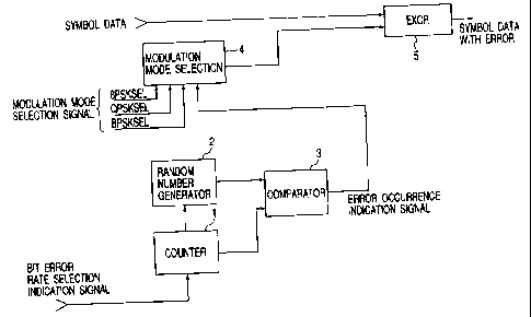
As shown in the block diagram in Figure 1, the dummy error
addition circuit according to the embodiment of the present
invention is provided with a variable counter 1 that receives a clock
signal and bit error rate selection signal and sends a count value and
carrier based on the bit error rate, a random number generator 2
that receives the carrier output from the variable counter 1 and
sends a series of random number values and a comparator 3 that
compares the count value output from the variable counter 1 and the
random number value output from the random number generator 2
and outputs an error pulse as a signal indicating the timing of
occurrence of an error when these two values match.
The dummy error addition circuit according to the embodiment
of the present invention is further provided with a modulation mode
selection circuit 4 that receives the error pulse and sends an
inversion indication signal based on the indicated modulation mode
and a bit inversion circuit 5 that receives the inversion indication
signal and symbol data, selectively applies bit inversion to the
symbol data and adds a dummy error thereto.
CA 02349854 2001-05-04
7 _
Figure 2 illustrates a specific configuration example of the
variable counter 1, the random number generator 2 and the
comparator 3 that form a partial block (lower part) of the dummy
error addition circuit shown in Figure 1.
The variable counter 1 is configured by n 4-bit binary counters
10-1 to 10-n that performs counts 0 to 2'111-1 (maximum) in response
to an input CLK as a whole and an n-input selector 11 that selects
one of n inputs X 1 to Xn according to a bit error rate selection
indication signal (signals of codes 0, 1, 2, ..., n corresponding to the
error rate) and outputs as Y. Furthermore, the random number
generator 2 is configured by a PN data generator (PNG) 21 that
generates a series of 4n-bit pseudo-random numbers (PN) and a
latch 22 that stores PN data output from the PN data generator 21,
enabled by the carrier (carrier output from any one of the n binary
counters) output from the selector 11 in the variable counter 1.
Furthermore, the comparator 3 is made up of n 2-input comparators
30-1, 30-2, 30-3, ..., 30-n (that operate in such a way as to generate
a pulse when two input values match) that receives lower 4 bits,
lower 8 bits, lower 12 bits., ..., lower 4n bits of a binary 4n-bit signal
output from the random number generator 2 and the n binary
counters 10-1 to 10-n, respectively as inputs and an n-input selector
31 that selects one of the outputs of n comparators 30-1 to 30-n
according to a bit error rate selection indication signal (code 1 to n)
input and extracts the output as an error occurrence indication
signal (error pulse). The circuit shown in Figure 2 has a
CA 02349854 2001-05-04
p -
...,
configuration assuming the case where one of 1/2", 1/28, 11212,
1/2"n is selected as the bit error rate. n 4-bit binary counters in the
variable counter 1 are connected vertically so that a carrier output
CO of one preceding stage is transmitted to a carrier input Cl of
another stage that follows and so on, forming a 4n-bit binary
synchronous counter as a whole. At the time of a full count, the
4-bit binary counters 10-1, 10-2, 10-3, ..., 10-n each output a
carrier (here "L" signal) from their respective CO at the time of 24, 28,
212, ..., 24n count, respectively. Operation when error rate 1/212 is
selected will be explained below by way of example. In this case, a
code "3" of the error rate selection indication signal is applied to the
selector 11 in the variable counter 1 and the SEL terminal of the
selector 31 in the comparator 3. At this time, a carrier from the CO
of the binary counter 10-3 is selected by the selector 11 and
extracted from Y thereof, then applied to the CL of all binary
counters 10-1 to 10-n and at the same time this carrier is applied to
the EN of the latch 22 in the random number generator 2.
Therefore, the variable counter 1 ends the count at 2121 and is
initialized (zero-count) at the next clock and then the same count is
restarted. At the same time, the latch 22 in the random number
generator 2 latches a new PN signal and outputs the PN signal to P 1
to P4n. In this way, until the carrier output from the variable
counter 1 is input, the latch 22 sends the PN data stored before the
carrier is input. Thus, in the above example, after the variable
counter 1 counts 212-1, the latch 22 newly stores PN data output
CA 02349854 2001-05-04
9 _
from the PN data generator 2 1 instead of the PN data stored
previously.
Furthermore, in the comparator 3 the selector 3 1 in the
comparator 3 selects the output of the comparator 30-3 (because
code "3" is input to SEL of the selector 31). At this time, the lower
12 bits P I to P12 of the 4n-bit PN data output from the random
number generator 2 and the lower 12 bits Q 1 to Q 12 of the 4n-bit
count value output from n binary counters are input to the
comparator 30-3. Therefore, the comparator 30-3 compares the
12-bit count value incremented for every clock input from 0 to 212-1
and a 12-bit random number value (value of one of. 0 to 212-1)
retained by the latch 22 for this count period.
Then, a pulse is output when both input values match once
every 212 times and that pulse is fetched as an error pulse via the
selector 3 1.
Therefore, when the bit error rate is set to 1/212, an error pulse
is randomly output from the comparator 3 once every 212 times on
average. The same holds true with a case where another bit error
rate is selected, for example, when the bit error rate is set to 1/28 or
1/24i1 , an error pulse is randomly output once every 28 times (0 to
28-1) or once every 24n times (0 to 241t-1).
The above circuit configuration example uses a 4-bit binary
counter, but it is naturally possible to use a decimal counter, and in
this case, it is possible to set the bit error rate to any one of 1/ 10"
(N=1, 2, 3,..., n). In this case, an error pulse is randomly output
CA 02349854 2001-05-04
-
once every 10" (0 to 999 === 99) on average. In the example above,
PNG that generates a PN signal, a pseudo-random number series, is
used as the random number generator, but it is naturally possible to
A/D-convert an analog noise signal generated by thermal noise and
5 fetch a digital random number series.
Therefore, this means that the variable counter 1, random
number generator 2 and comparator 3, as a whole, constitute error
pulse generating means that randomly generates an error pulse at a
specified bit error rate.
10 As shown in Figure 3, the modulation mode selection circuit 4
is configured by a PN data generator 41 that receives an error pulse
and outputs an error addition bit selection signal (the error addition
bit selection signal is also described as PNSELI and PNSELO and
illustrate a case where 2 bits are used), which is PN data, a bit
selector 40 that receives the PN data output from the PN data
generator 41 and randomly selects a bit to add an error and AND
gates 46a, 46b and 46c that receive the error pulse and the output
from the bit selector 40 as inputs.
The bit selector 40 is provided with an inverter 42a that
logically inverts the error addition bit selection signal PNSELO, an
inverter 42b that logically inverts the error addition bit selection
signal PNSELI, an inverter 42c that logically inverts the error
addition bit selection signal PNSELI, an AND gate 43a that carries
out the logical AND between the output of the inverter 42a and the
output of the inverter 42b and an AND gate 43b that carries out the
CA 02349854 2001-05-04
- 11 -
logical AND between the error addition bit selection signal PNSELO
and the output of the inverter 42c.
The bit selector 40 is further provided with an AND gate 44a
that carries out the logical AND between an 8PSK selection signal
(the 8PSK selection signal is also described as 8PSKSEL) and the
output of the AND gate 43a, an AND gate 44b and 44d that carries
out the logical AND between the error addition bit selection signal
PNSELO and the QPSK selection signal (the QPSK selection signal is
also described as QPSKSEL), an AND gate 44c that carries out the
logical AND between the 8PSK selection signal and the output of the
AND gate 43b and an AND gate 44e that carries out the logical AND
between the error addition bit selection signal PNSELI and the 8PSK
selection signal.
The bit selector 40 is further provided with an OR gate 45a that
carries out the logical OR between the output of the AND gate 44a,
the output of the AND gate 44b and the BPSK selection signal (the
BPSK selection signal is also described as BPSKSEL), an OR gate 45b
that carries out the logical OR between the output of the AND gate
44c and the output of the AND gate 44d, and the output of the OR
gate 45a is sent to an AND gate 46a, the output of the OR gate 45b is
sent to an AND gate 46b, the output of the AND gate 44e is sent to
an AND gate 46c and an error pulse is output from the AND gates
46a, 46b and 46c whose gate has been opened.
Thus, the truth table of the modulation mode selection circuit
4 is as shown in Figure 4. That is, when 8PSKSEL is selected by the
CA 02349854 2001-05-04
- 12 -
modulation mode selection signal and the error addition bit selection
signals PNSELl and PNSELO are "00," this is the case where an error
is added to the LSB of the 8PSK symbol data, and the output of the
OR gate 45a becomes a high potential, the output of the OR gate 45b
becomes a low potential, the output of the AND gate 44e becomes a
low potential, and in this way only the AND gate 46a remains open,
the LSB of the 8PSK symbol data remains selected, and thereby an
error pulse is output from the AND gate 46a.
When 8PSKSEL is selected by the modulation mode selection
signal and the error addition bit selection signals PNSELl and
PNSELO are "01," this is the case where an error is added to the 2nd
bit of the 8PSK symbol data, and the output of the OR gate 45a
becomes a low potential, the output of the OR gate 45b becomes a
high potential, the output of the AND gate 44e becomes a low
potential, and in this way only the AND gate 46b remains open, the
2nd bit of the 8PSK symbol data remains selected, and thereby an.
error pulse is output from the AND gate 46b.
When 8PSKSEL is selected by the modulation mode selection
signal and the error addition bit selection signals PNSELl and
PNSELO are "lx" (x can be either "0" or "1"), this is the case where an
error is added to the MSB of the 8PSK symbol data, and the output
of the OR gate 45a becomes a low potential, the output of the OR
gate 45b becomes a low potential, the output of the AND gate 44e
becomes a high potential, and in this way only the AND gate 46c
remains open and the MSB of the 8PSK symbol data remains
CA 02349854 2001-05-04
- 13 -
selected, and thereby an erroi- pulse is output from the AND gate
46c.
When QPSKSEL is selected by the.modulation mode selection
signal and the error addition bit selection signals PNSELI and
PNSELO are "x0," this is the case where an error is added to the LSB
of the QPSK symbol data, and the output of the OR gate 45a
becomes a high potential, the output of the OR gate 45b becomes a
low potential, the output of the AND gate 44e becomes a low
potential, and in this way only the AND gate 46a remains open, the
LSB of the QPSK symbol data remains selected, and thereby an error
pulse is output from the AND gate 46a.
When QPSK is selected by the modulation mode selection
signal and the error addition bit selection signals PNSELI and
PNSELO are "xl," this is the case where an error is added to the MSB
of the QPSK symbol data, and the output of the OR gate 45a
becomes a low potential, the output of the OR gate 45b becomes a
high potential, the output of the AND gate 44e becomes a low
potential, and in this way only the AND gate 46b remains open, the
MSB of the QPSK symbol data remains selected, and thereby an
error pulse is output from the AND gate 46b.
When the BPSKSEL is selected by the modulation mode
selection signal and the error addition bit selection signals PNSEL 1
and PNSELO are "xx," the output of the OR gate 45a becomes a high
potential, the output of the OR gate 45b becomes a low potential, the
output of the AND gate 44e becomes a- low potential, and in this way
CA 02349854 2001-05-04
- 14 -
only the AND gate 46a remains open and an error pulse is output
from the AND gate 46a.
In this way, an inversion indication signal is output from the
modulation mode selection circuit 4. This inversion indication
signal randomly indicates a bit to add an error based on the P data
output from the PN data generator 41 and an error pulse is output to
the indicated bit.
Therefore, the modulation mode selection circuit 4 constitutes
the bit selecting means that randomly selects a bit to add an error
from among bits in the symbol data based on the selected
modulation mode at intervals based on the bit error rate based on
the PN data output from the PN data generator 41.
As shown in Figure 3, the bit inversion circuit 5 is provided
with exclusive-OR circuits 51a, 51b and 51c that are supplied with
symbol data and the output from the AND gate 46a, the output from
the AND gate 46b and the output from the AND gate 46c are input,
respectively and symbol data with only 1 bit inverted and an error
added is output from the exclusive-OR circuits 51a, 51b and 51c.
In the dummy error addition circuit according to the
embodiment of the present invention, an 8PSK modulation baseband
signal, which is symbol data, is mapped on a phase plane as shown
in Figure 5(a) and there are 8 ways of combination of bits (0,0,0),
(0,0,1) to (1,1,1) that form symbols and these signals are converted
to signal constellation 0 to 7 on an I-Q plane. Likewise, Figure 5(b)
shows a signal constellation of a QPSK modulation baseband signal
CA 02349854 2001-05-04
- 15 -
and there are 4 ways of combination of bits (0,0), (0,1), (1,0) and (1,1)
that form symbols and these are converted to signal constellation 0
to 3 on an I-Q plane. Likewise, Figure -5(c) shows a signal
constellation of a BPSK modulation baseband signal and there is a
combination of bits (0) and (1) that form symbols and these are
converted to signal constellation 0, 1.
Now, a case where an 8PSK modulation is selected and symbol
data " 101" is input will be explained as an example. In this state,
when the error addition bit selection signal PNSELl and PNSELO are
"lx," that is, when the MSB is selected, the MSB of the symbol data
"101" is inverted and the symbol data becomes "001" with 1 bit
carrying an error. On the other hand, when the error addition bit
selection signal PNSELl and PNSELO are "01," that is, when the 2nd
bit is selected, the 2nd bit of the symbol data "101" is inverted and
the symbol data becomes "111" with 1 bit carrying an error. When
the error addition bit selection signal PNSEL 1 and PNSELO are "00,"
that is, the LSB is selected, the LSB of the symbol data "101" is
inverted and the symbol data becomes "100" with 1 bit carrying an
error. Similar estimation can be applied when other symbol data is
input.
Now, a case where a QPSK modulation is selected and symbol
data "01" is input will be explained as an example. In this state,
when the error addition bit selection signal PNSELI and PNSELO are
"xl," that is, when the MSB is selected, the MSB of the symbol data
"01" is inverted and the symbol data becomes " 1 1" with 1 bit carrying
CA 02349854 2001-05-04
- 16 -
an error. On the other hand, when the error addition bit selection
signal PNSELI and PNSELO are "x0," that is, when the LSB is
selected, the LSB of the symbol data "01" is inverted and the symbol
data becomes "00" with 1 bit carrying an error. Similar estimation
can be applied when other symbol data is input.
Now, a case where a BPSK modulation is selected and symbol
data "1" is input will be explained as an example. In this state,
when the error addition bit selection signal PNSELl and PNSELO are
"xx," the symbol data " 1" is inverted to "0" with 1 bit carrying an
error. On the other hand, when the symbol data "0" is input, the
symbol data "0" is inverted to " 1" with 1 bit carrying an error.
As explained above, the dummy error addition circuit according
to the embodiment of the present invention randomly adds a dummy
error to a bit randomly selected on a baseband signal at a set bit
error rate without performing direct modulation. It is possible to
check the performance of a decoder by supplying symbol data with a
dummy error added to the decoder and make the decoder perform
decoding. As a result, this embodiment allows effective design
during the development of a receiver.
As shown above, the configuration and operation of the-present
invention has been explained by taking as an example, bit error
addition to 8PSK, QPSK and BPSK symbol data according to the
modulation system exclusively used in a digital broadcasting receiver.
Application of the present invention, however, is not limited to bit
error addition to multi-phase PSK symbol data. The technological
CA 02349854 2001-05-04
- 17 -
scope of the present invention should not be limited to the above
illustr~tive embodiments alone, but should be interpreted to be
applicable to error addition to multi-value orthogonal modulation
symbol data without departing from the principle thereof.
It goes without saying that the dummy error addition circuit
according to the embodiment of the present invention is also
applicable to a cellular telephone set.
INDUSTRIAL APPLICABILITY
As explained above, the dummy error addition circuit according
to the present invention can add dummy errors to randomly selected
bits on a baseband signal at a rate based on a set bit error rate and
can therefore be used for a performance check of a decoder.
,, .