Note: Descriptions are shown in the official language in which they were submitted.
CA 02349926 2004-08-10
-1-
AN OPTfCAL BUS
BACKGROUND OF THE INVENTION
FIELD OF THE INVENTION
This invention relates generally to optical communications and, more
particularly,
to the coupling and distribution of optical signals.
BACKGROUND OF THE INVENTION
In the area of optical communications, there is a need to distribute, or
redirect,
optical streams (gigabit per second rates or higher) from one, or more, source
devices to
one, or more, destination devices. One solution is to first convert an optical
signal to its
electrical equivalent and then apply the resulting electrical signals) to an
electrical bus,
which is used to interconnect the various devices. (As known in the art, an
electrical bus
comprises one or more electrical conductors for distributing one or more
electrical signals
from one, or more, source devices to one, or more, destination devices.)
Unfortunately,
there are added costs involved with this electrical conversion, e.g., there is
the dollar cost
of the electrical components themselves that are required to convert the
signal from an
optical form to an electrical form and back again - and there is also a
performance cost in
terms of having to process high-speed gigabit optical signals in the
electrical domain that
may introduce distortion and delay.
SUMMARY OF THE INVENT10N
An optical bus for distributing optical signals. In particular, a light guide
comprises an array of embedded elements for coupling light between a plurality
of ports
of the light guide.
In one embodiment, the light guide is an optical fiber comprising an
integrated
array of thermal switches at predetermined intervals.
In another embodiment, the light guide is an optical fiber comprising an
integrated
array of optical beam splitters at predetermined intervals.
CA 02349926 2004-08-10
la
In accordance with one aspect of the present invention there is provided an
optical
bus, comprising: a light guide comprising an optical channel for propagating
an optical
signal; a plurality of elements embedded along said optical channel, each of
said elements
comprising two input ports for receiving the optical signal from said optical
channel and for
receiving a second optical signal from a respective associated access port in
said light guide,
wherein each of said elements is controllable to propagate one of the two
input optical signals
along said optical channel and block the other of the two input optical
signals from further
propagation.
BRIEF DESCRIPTION OF THE DRAWINGS
CA 02349926 2001-06-08
-2-
FIG. 1 shows an illustrative embodiment of an optical bus in accordance with
the
principles of the invention;
FIGS. 2 and 3 show other views of the embodiment of FIG. 1;
FIG. 4 shows another embodiment of an optical bus in accordance with the
principles of the invention;
FIG. 5 shows another view of the embodiment of FIG. 4;
FIG. 6 shows another embodiment of an optical bus in accordance with the
principles of the invention; and
FIGS. 7 and 8 show illustrative applications of the inventive concept.
DETAILED DESCRIPTION
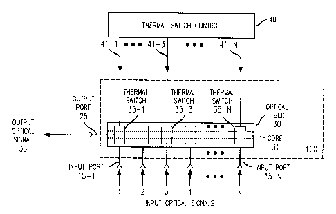
An illustrative embodiment of an optical bus in accordance with the principles
of
the invention is shown in FIG. 1. Optical Bus 100 comprises a light guide with
embedded elements for coupling light between a plurality of ports of the light
guide.
Illustratively, the light guide is represented by optical fiber 30 (presumed
to be a single
I S mode optical fiber), and the embedded elements are represented by a
plurality of thermal
switches 35-1 through 35-N spaced at predetermined (e.g., uniform) intervals
in optical
fiber 30 (also referred to as an "in-line thermal optical bus"). Each thermal
switch is
controlled via thermal switch control element 40 (control signals 41-1 through
41-N).
For reference purposes, lower numbered thermal switches are considered
"upstream" of
higher numbered thermal switches (or, higher numbered thermal switches are
"downstream" of lower numbered thermal switches). For example, thermal switch
35-I
is upstream of thermal switch 35-3, while the latter is downstream of thermal
switch 35-
1. Other than the inventive concept, the elements shown in FIG. 1 are well-
known and
will not be described in detail. For example, an optical fiber comprises a
core and a
cladding. Similarly, a thermal switch, by itself, is known in the art, (e.g.,
a thermal switch
can be purchased from Kymata Ltd. and information can be found at
"www.kymata.com"). Likewise, thermal switch control 40 represents a stored-
program
control based-processor (e.g., a microprocessor) and associated memory (both
not shown)
for providing control signals 41-1 through 41-N. It is presumed that thermal
switch
control 40 is suitably programmed using conventional programming techniques,
which,
CA 02349926 2001-06-08
-3-
as such, will not be described herein.
Optical fiber 30 comprises N input ports (15-1 through 15-N) along its length
(physically, each input port of optical fiber 30 is an access point, window,
or hole, to let
in light). Each thermal switch has two input ports and one output port (not
explicitly
shown in FIG. I ), i.e., each thermal switch is a I x2 switch. One input port
of each
thermal switch is coupled through one of the N input ports of optical fiber 30
to receive
one of N input optical signals (from any of N optical sources (not shown)).
The other
input port of each thermal switch is coupled to the core 31 of optical fiber
30. As can be
observed from FIG. 1, effectively this other input port of each thermal switch
is coupled
to the output port of the next downstream thermal switch. For example, one
input port of
thermal switch 35-1 is coupled to input port 15-1 for receiving input optical
signal 1, and
the other input port of thermal switch 35-1 is coupled (via that portion of
core 31 of
optical fiber 30) to the output port of thermal switch 35-2. The output port
of thermal
switch 35-1 is coupled to that portion of core 31 of optical fiber 30 that
provides the
output optical signal 36, via output port 25. (It should be noted that each
input optical
signal may comprise one or more wavelengths, e.g., an optical signal may have
a single
wavelength or have multiple wavelengths (a WDM (wavelength division
multiplexed)
signal).)
Thermal switch control 40 controls the state of each thermal switch. As used
herein, when a thermal switch is "ON," optical energy is coupled from that
input port of
the thermal switch that is coupled to a corresponding input port of optical
fiber 30 to the
output port of the thermal switch (and hence into core 31 of optical fiber
30).
Conversely, when a thermal switch is "OFF," optical energy is coupled from
that input
port of the thermal switch that is coupled to core 31 of optical fiber 30 to
the output port
of the thermal switch (and hence back into core 31 of optical fiber 30 for
transmission
further upstream). Consequently, when a thermal switch is "OFF," light is
propagated
through optical fiber 30, going upstream from one thermal switch to the next
upstream
thermal switch. Conversely, when a thermal switch is "ON," light is let into
the core of
the optical fiber and light from any other downstream thermal switch is
blocked. For
example, consider thermal switch 35-3. When thermal switch 35-3 is controlled
to be
..._...~~..~..~...~.~., ~-...-.w....~...-w... . ._.... ..
CA 02349926 2001-06-08
-4-
"ON," light applied via input port 15-3 is propagated into core 31 of optical
fiber 30 via
thermal switch 35-3. Assuming that thermal switches 35-1 and 35-2 are "OFF,"
this light
is propagated through optical fiber 30 to become output optical signal 36
(albeit with
some attenuation). Since thermal switch 35-3 is "ON," any downstream light
propagating
through optical fiber 30, e.g., via downstream thermal switches 35-4 through
35-N, is
blocked. Thus, in this illustrative embodiment, it is assumed that only one
thermal switch
is "ON" at a time to permit light from the corresponding input port to enter
optical fiber
30 for propagation through optical fiber 30 (and any upstream thermal
switches) to
emerge as the output optical signal 36. It should be noted that to compensate
for any
attenuation loss of the input optical signal, an optical amplifier (not shown
in FIG. 1) may
be used to amplify output optical signal 36. However, it is known that a
thermal switch
has a low amount of attenuation loss, which may relegate the use of an optical
amplifier
to larger optical bus structures.
Another view of the embodiment of FIG. 1 is shown in FIG. 2. In the latter,
optical fiber 30 is shown receiving N input optical signals along the length
of optical fiber
30 (where each of the corresponding N input ports are located). Embedded
thermal
switches 35-1 through 35-N are represented by slash marks "/." Illustratively,
thermal
switch 35-3 is "ON," which (as described above) lets input optical signal 3
into optical
fiber 30, which subsequently emerges as output optical signal 36.
Similarly, another view of the embodiment of FIG. 1 is shown in FIG. 3. Here,
a
portion of optical fiber 30 is shown comprising the first three thermal
switches, 35-1, 35-
2 and 35-3. Each of these thermal switches is coupled to a corresponding input
port as
illustrated by input ports 15-1, 15-2 and 15-3. Illustratively, thermal switch
35-3 is "ON"
and thermal switches 35-1 and 35-2 are "OFF," which (as described above) lets
input
optical signal 3 into optical fiber 30, which subsequently emerges as output
optical signal
36. In other words, optical fiber 30 represents a light guide comprising an
optical channel
(core 31 of optical fiber 30) for conveying light such that a plurality of
elements are
embedded along the optical channel, each embedded element disposed within the
light
guide for receiving light either from an associated access point of the light
guide (e.g., 15-
l, 15-2, 15-3, etc.) or from the optical channel (e.g., core 31 of optical
fiber 30).
CA 02349926 2001-06-08
- 5 -
An illustrative manufacturing procedure for a thermal optical bus as
illustrated in
FIGS. 1 - 3 is to use industry standard Silica-on-Silicon techniques (or other
appropriate
technology) and assemble embedded thermal-optical 1X2 switches into an in-line
array
within a light guide structure. (Silica glass is compatible with single mode
fibers.) The
thermal switch array utilizes multiple thermal optical switches placed in-line
with an
associated input access point for receiving input optical signals along the
length of the
light guide structure. The individual thermal optical switches are controlled
through
individual heater control signals associated with each input signal position.
As noted above, when a thermal switch is "ON," downstream light is blocked.
This allows an input optical signal having one or more wavelengths (e.g., a
WDM signal)
to be propagated to the output port of the optical bus without mixing with
other input
optical signals. However, since the downstream light is blocked, an optical
bus
comprising integrated thermal switches is not conducive to generating a WDM
signal
from different input optical signals, each having a different wavelength.
In contrast, another illustrative embodiment of an optical bus in accordance
with
the principles of the invention is shown in FIG. 4. Optical Bus 200 comprises
a light
guide with embedded elements for coupling light between a plurality of ports
of the light
guide. Illustratively, the light guide is represented by optical fiber 230
(presumed to be a
single mode optical fiber), and the embedded elements are represented by a
plurality of
optical beam splitters (splitters) 235-1 through 235-N spaced at predetermined
(e.g.,
uniform) intervals in optical fiber 230 (also referred to as an "in-line
sputter optical bus").
For reference purposes, lower numbered splitters are considered "upstream" of
higher
numbered splitters (or, higher numbered splitters are "downstream" of lower
numbered
sputters). For example, sputter 235-1 is upstream of sputter 235-3, while the
latter is
downstream of splitter 235-1. Other than the inventive concept, the elements
shown in
FIG. 4 are well-known and will not be described in detail. For example, an
optical fiber
comprises a core and a cladding. Similarly, a sputter, by itself, is known in
the art.
Optical fiber 230 comprises N input ports (215-1 through 215-N) along its
length
(again, physically, each input port of optical fiber 230 is an access point,
window, or hole,
to let in light). Each sputter has two input ports and one output port (not
explicitly shown
CA 02349926 2001-06-08
-6-
in FIG. 4). One input port of each splatter is coupled through one of the N
input ports of
optical fiber 230 to receive one of N input optical signals (from any of N
optical sources
(not shown)). The other input port of each sputter is coupled to core 231 of
optical fiber
230. As can be observed from FIG. 4, effectively this other input port of each
sputter is
coupled to the output port of the next downstream sputter. For example, one
input port of
sputter 235-1 is coupled to input port 215-l for receiving input optical
signal 1 (via
selector 220 (described below)), the other input port of sputter 235-1 is
coupled (via that
portion of core 231 of optical fiber 230) to the output port of splatter 235-
2. The output
port of splatter 235-1 is coupled to that portion of core 231 of optical fiber
230 that
provides the output optical signal 236, via output port 225.
Unlike the embodiment illustrated in FIG. 1, a splatter does not block light,
i.e.,
some light is reflected and some light is passed through. Thus, with respect
to optical bus
200 (ignoring for the moment selector 220) light applied at any input port
will mix with
light applied at other input ports. As such, an optical bus comprising
splatters is useful in
IS (WDM) applications, since light of different wavelengths can be applied to
different ones
of the input ports 215-I through 215-N with the result that output optical
signal 236 is a
WDM signal. (It should also be noted that, strictly speaking, the input ports
of optical
fiber 230 also serve as output ports, since some light is reflected. In other
words, they are
bi-directional ports since some light from downstream splatters will appear on
the
upstream input ports. Indeed, this feature is taken advantage of in one of the
optical
applications described further below.)
However, in the situation where the input optical signals all have the same
wavelength it is necessary to block light from certain ones of the input ports
to prevent
inadvertent mixing of the input optical signals within core 231 of optical
fiber 230.
(Indeed, it may even be advantageous to do this in a WDM application.) Thus,
selector
220 is used to block the input optical signals. Selector 220 (control signals
not shown)
enables one input optical signal at a time to be applied to optical fiber 230.
Although not
necessary to the inventive concept, selector 220 is, e.g., an array of thermal
1x2 switches,
with one of the input ports of each thermal switch unused. Alternatively,
selector 220 is
an array of liquid crystal pixel elements such as described and shown in the
co-pending,
CA 02349926 2001-06-08
commonly assigned U.S. Patent application of Ranganath et al., entitled "An
Optical
CrossBar Switch," Application No. 09/478630, filed on January 6, 2000. Control
circuitry for either element is straightforward and is not described herein.
Similar to the
description of optical bus 100, each element of selector 220 can be referred
to as having
an "ON" state, i.e., optical energy is coupled to the corresponding input port
of optical
fiber 230, and an "OFF" state, i.e., light is blocked from the corresponding
input port of
optical fiber 230. This is illustrated in FIG. 4, where selector 220, element
3, is turned
"ON" to allow light to enter optical fiber 230 via input port 215-3. Other
elements of
selector 220 are "OFF." As such, only light from input optical signal 3
transits optical
fiber 230 to become output optical signal 236 (albeit with some attenuation).
Thus, in a
non-WDM application, it is assumed that only one element of selector 220 is on
at a time
to permit light from the corresponding input port to enter optical fiber 230
for
propagation through optical fiber 230 to emerge as the output optical signal
236. (It
should be noted that selector 220 can be controlled so as to let more than one
input
optical signal into optical fiber 230, if so desired.)
Another view of the embodiment of FIG. 4 is shown in FIG. 5. In the latter,
optical fiber 230 is shown receiving any one of N input optical signals along
the length of
optical fiber 230 (where each of the corresponding N input ports are located).
Embedded
sputters 235-1 through 235-N are represented by slash marks "/."
Illustratively, selector
220 (as described above) lets input optical signal 3 pass through into optical
fiber 230 and
blocks all other input optical signals. Input optical signal 3 subsequently
emerges as
output optical signal 236.
This embodiment of an optical bus utilizes embedded sputter elements that may
have a significant amount of attenuation loss to an input optical signal. (For
example, an
optical beam sputter may have a 60/40 ratio, i.e., 60% of the light is let
through, while
40% of the light is reflected.). As such, an optical amplifier may be used to
amplify the
output optical signal in order to compensate for loss through the splitters.
This is
illustrated in FIG. 6, which shows output optical signal 236 being applied to
optical
amplifier 250, which provides an amplified optical signal 251. (This is in
contrast to the
above-described optical bus 100, which utilizes thermal switch elements that
have lower
CA 02349926 2001-06-08
_ g _
forward light loss.)
An illustrative manufacturing procedure for a beam splitter optical bus as
illustrated in FIGs. 4 - 6 is to use industry standard Silica-on-Silicon
techniques (or other
appropriate technology) and assemble embedded optical beam splitter elements
into an
in-line array within a light guide structure. (Silica glass is compatible with
single mode
fibers.) The optical beam splitter array utilizes multiple optical beam
sputters placed in-
line with an associated input access point for receiving input optical signals
along the
length of the light guide structure. The individual optical beam splitters are
passive and
require no external control signals. The amount of coating on each optical
beam sputter
determines the ratio of reflected light to transmitted light, which is
predetermined by
design. Standard methods of fusion splicing, photolithography and reactive ion
etching
may be used to construct the optical bus.
Some illustrative applications of an optical bus in accordance with the
principles
of the invention are shown in FIGs. 7 and 8. FIG. 7 illustrates the use of an
optical bus as
1 S part of a programmable line build-out attenuator, which is used to receive
an input optical
signal of varying energy level (a "hot signal") and to provide an output
optical signal at a
predefined energy level. In particular, the programmable line build-out
attenuator
comprises optical bus 330, optical bus 340, selector 320, tap 335 and gain
control circuit
305, which further comprises photo detector 315 and analog-to-digital (A/D)
element
310. An input optical signal is applied to optical bus 340. The latter is
illustratively an
inline splitter optical bus (as shown in FIG. 4). As noted above, each sputter
both reflects
and transmits light. As such, as light passes through each splitter of optical
bus 340,
varying degrees of attenuation are introduced into the input optical signal.
Since each
sputter both reflects and transmits light, some light appears as an output
signal at, what
heretofore were referred to as the input ports of the optical bus. These are
shown in FIG.
7 as attenuation taps 0 dB (decibels), -S dB, -10 dB and -20 dB. Each of the
output
signals from the attenuation taps is applied to an element of selector 320.
The latter is
controlled by gain control circuit 305 via control lines 311, 312, 313 and
314. In this
example, it is assumed that gain control circuit 305 turns "ON" element 3, via
control line
313, of selector 320 to enable light to pass through to a corresponding input
port of
CA 02349926 2001-06-08
-9-
optical bus 330, which is also illustratively an inline splitter optical bus.
(However, it
could also be an inline thermal optical bus as illustrated in FIG. 1. In this
case, selector
320 is not needed and gain control circuit 305 controls each thermal switch
via control
signals 311, 312, 313 and 314.) Optical bus 330 provides an optical signal
(again at a
certain attenuation level) to tap 335, which provides the output optical
signal and also
provides an optical feedback signal to gain control circuit 305. The latter
receives the
optical feedback signal via photo detector 315, which converts the optical
signal into an
electrical signal that is provided to A/D converter element 310. Depending on
the level
of the optical feedback signal, A1D converter element 310 operates such that a
different
one of the control signals 31 l, 312, 313 and 314 is enabled to turn on a
particular element
of selector 320. Thus, the energy level of the output optical signal is
controlled by
selecting different ones of the attenuation taps of optical bus 340.
Turning now to FIG. 8, an optical tilt control application of an optical bus
in
accordance with the principles of the invention is shown. The optical tilt
control
comprises selectors 405, 410, and 41 S, and optical buses 440, 445, 450 and
430. It is
assumed for this application that all optical buses are of the inline sputter
optical bus.
This particular application takes advantage of the WDM capability of an inline
splitter
optical bus. Optical buses 440, 445 and 450, each receive an input optical
signal at a
different wavelength as provided by corresponding selectors 405, 410 and 415
(the
control signals for these selectors are not shown). In particular, an input
signal having a
wavelength R is provided to optical bus 440, an input signal having a
wavelength G is
provided to optical bus 445 and an input signal having wavelength B is
provided to
optical bus 450. Each optical bus provides their input signal (in attenuated
form) to a
corresponding input port of optical bus 430. Optical bus 430 mixes each
received signal
to provide the flat tilt output signal, which is a WDM signal.
As described above, and in accordance with the invention, an optical bus
provides
significant advantages over mechanical or electrical bus construction,
resulting in low
power, no moving parts (robustness), zero cross talk and low loss. In
addition, the optical
nature of this design allows any Ethernet framing to be preserved and thus
preserves
Quality of Service (QoS), VLAN (virtual local area network) tagging and
payload. Due
CA 02349926 2001-06-08
- l~-
to the optical design of the bus, standardized link aggregation protocols may
be applied as
separate gigabit links. Applications for metro-ring, metro access and
enterprise access is
possible with this bus design, and at a reduced cost.
The foregoing merely illustrates the principles of the invention and it will
thus be
appreciated that those skilled in the art will be able to devise numerous
alternative
arrangements which, although not explicitly described herein, embody the
principles of
the invention and are within its spirit and scope. For example, although a
light guide was
illustrated in the context of an optical fiber, the light guide could also be
formed using
optical integrated circuit techniques. Similarly, although the illustrative
embodiment
described the use of embedded elements such as thermal switches and optical
beam
splitters, other elements may be used such as "optical bubble-jet technology"
elements
formed into an in-line array within a light guide structure. Such an array
utilizes multiple
optical bubble elements placed in-line with an associated input window for
receiving
input optical signals along the length of the light guide structure. The
individual optical
bubble elements are driven through individual control signals associated with
each
individual input signal position.