Note: Descriptions are shown in the official language in which they were submitted.
, CA 02350191 2001-06-12
1
BUS BAR WITH FREQUENCY-FILTERING GEOMETRY
BACKGROUND OF THE INVENTION
1. Field of the invention:
The present invention relates to a bus bar having a geometry designed
for filtering desired signal frequencies.
2. Brief description of the prior art:
The prior art has already proposed bus bars configured to create a high
capacitive region of low impedance for filtering high frequency noise and
attenuate
voltage transients. For that purpose, a region of high static capacitance is
formed
by inserting a high dielectric material in the form of wafers, chips or disks
between
two electrically conducting plates. For example:
US Patent No. 4,436,953 granted to Gottlieb on March 13, 1984
describes miniature bus bar assemblies which incorporate discrete
capacitive elements having a high dielectric constant. These capacitive
elements are preferably metallized ceramic wafers bonded between a
pair of bus bar conductors.
US Patent No. 4,440,972 (Taylor) issued on April 3'~, 1984 proposes
miniature bus bars in which capacitor ribbons with discrete capacitive
CA 02350191 2001-06-12
2
elements are retained within the insulating layer. These capacitor
ribbons are mounted between a pair of bus bar conductor plates with
the capacitive elements placed in electrical contact with the plates.
~ US Patent No. 4,584,768 granted to Tosti on April 29, 1986 relates to
a method for manufacturing a highly capacitive multilayer conductive
bar. Again, ceramic chips are used to improve the capacitance. These
chips are placed within the layers of the conductive bar.
-~ US Patent No. 5,185,690 (Hernandez) issued on September 24, 1991
discloses a bus bar including conductive layers and a high capacitance
flexible dielectric sheet material between these conductive layers. The
high capacitance dielectric sheet comprises high dielectric chips or
pellets of relatively small area and thickness arranged in a planar array.
These high dielectric constant chips are spaced apart by a small
distance.
US Patent No. 5,365,424 granted to Deam et al., on November 15,
1994 suggests the use of a low impedance (high capacitance) bus
structure involving a laminated plate assembly. This patent mentions
that the inductive impedance substantially attenuates the high
frequency response of a bus.
The above prior art references present no high frequency model for any
structure, and the performance of these structures is likely to be very
irregular from
the frequency response and filtering points of view. Also, these structures
will not
enable the construction of a bus bar capable of producing desired frequency
attenuation for high frequency signals while conducting DC signal without
attenuation.
CA 02350191 2001-06-12
3
Also, low pass filters are currently used in electrical circuits to suppress
noise. In high impedance and high frequency circuits, pi-network filters are
widely
used. A pi-network includes two shunt capacitors and an inductor connected in
series between the two capacitors. United States Patent 4,853,659 granted to
Kling
on August 1 St, 1989 describes a planar pi-network filter assembly. This
filter
assembly comprises capacitive structures formed on opposing surfaces of a
planar
inductive member. Each capacitive structure comprises a ground electrode
section,
a dielectric layer and a signal electrode. Preferably, the inductive member is
made
of ferrite material. The combination forms a capacitor-inductor-capacitor pi-
network.
OBJECT OF THE INVENTION
An object of the present invention is to provide a laminated conductor
assembly presenting a desired frequency-filtering feature obtained by
manipulating the geometry of the conductor(s).
SUMMARY OF THE INVENTION
More specifically, in accordance with the present invention, there is
provided a laminated conductor assembly comprising an input section, an output
section, and a superposition of alternate electrically conducting and
electrically
insulating layers. The electrically conducting layers present a geometry which
defines both capacitive and inductive structures, and these capacitive and
inductive structures form, between the input and output sections, a capacitive
and inductive frequency-filtering circuit.
In accordance with a preferred embodiment of the laminated conductor
assembly, the electrically conducting layers comprise respective, superposed
first
CA 02350191 2001-06-12
4
end portions for defining first capacitive structures, respective, superposed
second end portions opposite to the first end portions for defining second
capacitive structures, and respective narrower bridge portions for
interconnecting
the first and second end portions of the corresponding electrically conducting
layers and for defining respective inductive structures. Advantageously, at
least
a part of the narrower bridge portions are laterally offset with respect to
each
other.
The present invention further relates to a laminated direct current bus
bar, comprising an input section, an output section, and a superposition of
alternate electrically conducting plates and electrically insulating films.
This
superposition comprises a first electrically conducting ground plate, an
electrically
conducting positive plate, an electrically conducting negative plate, a second
electrically conducting ground plate, a first electrically insulating film
interposed
between the first ground plate and the positive plate, a second electrically
insulating film interposed between the positive plate and the negative plate,
and
a third electrically insulating film interposed between the negative plate and
the
second ground plate. The first ground plate, the positive plate, the negative
plate
and the second ground plate have a geometry which defines both capacitive and
inductive structures, and these capacitive and inductive structures form,
between
the input and output sections, a capacitive and inductive frequency-filtering
circuit.
According to a preferred embodiment of the laminated bus bar, the first
ground plate, the positive plate, the negative plate and the second ground
plate
comprise respective, superposed first end portions for defining first
capacitive
structures, respective, superposed second end portions opposite to the first
end
portions for defining second capacitive structures, and respective narrower
bridge
portions for interconnecting the first and second end portions of the
CA 02350191 2001-06-12
corresponding plates, these narrower bridge partions defining respective
inductive structures.
Preferably, the narrower bridge portions of the positive and negative
5 plates are laterally offset with respect to each other and with respect to
the
narrower bridge portions of the first and second ground plates.
According to another preferred embodiment:
-~ the input section comprises a tab of the first end portion of the positive
plate
and a tab of the first end portion of the negative plate;
~ the output section comprises a tab of the second end portion of the positive
plate and a tab of the second end portion of the negative plate;
~ the first ground plate, the positive plate, the negative plate and the
second
ground plate have respective first and second ends;
~ the tab of the first end portion of the positive plate is a laterally
extending tab
situated at the first end of the positive plate;
~ the tab of the first end portion of the negative plate is a laterally
extending tab
situated at the first end of the negative plate;
-~ the tab of the second end portion of the positive plate is a laterally
extending
tab situated at the second end of the positive plate; and
the tab of the second end portion of the negative plate is a laterally
extending
tab situated at the second end of the negative plate.
CA 02350191 2001-06-12
6
In accordance with a further preferred embodiment of the laminated bus
bar, the first and second ground plates are electrically interconnected, the
first
end portion of the positive plate and the first end portion of the first
ground plate
define with the first film a first shunt capacitor structure, the first end
portion of
the positive plate and the first end portion of the negative plate define with
the
second film a second shunt capacitor structure, the first end portion of the
negative plate and the first end portion of the second ground plate define
with the
third film a third shunt capacitor structure, the narrower bridge portion of
the
positive plate forms a first inductor structure, the narrower bridge portion
of the
negative plate forms a second inductor structure, the narrower bridge portions
of the first and second ground plates form a third inductor structure, the
second
end portion of the positive plate and the second end portion of the first
ground
plate define with the first film a fourth shunt capacitor structure, the
second end
portion of the positive plate and the second end portion of the negative plate
define with the second film a fifth shunt capacitor structure, and the second
end
portion of the negative plate and the second end portion of the second ground
plate define with the third film a sixth shunt capacitor structure.
In accordance with a further preferred embodiment of the laminated bus
bar, the first and second ground plates both have first and second ends and
are
longer than the positive and negative plates and the first, second and third
films,
the first ends of the first and second ground plates are interconnected and
the
second ends of the first and second ground plates are interconnected.
The foregoing and other objects, advantages and features of the present
invention will become more apparent upon reading of the following non
restrictive
description of a preferred embodiment thereof, given for the purpose of
illustration only with reference to the accompanying drawings.
CA 02350191 2001-06-12
7
BRIEF DESCRIPTION OF THE DRAWINGS
In the appended drawings:
Figure 1 is a top plan view of the preferred embodiment of the bus bar
according to the present invention, having frequency-filtering features;
Figure 2 is a side elevation view of the bus bar of Figure 1;
Figure 3 is a top plan view of a lower ground plate of the bus bar of
Figures 1 and 2;
Figure 4 is a top plan view of a positive plate of the bus bar of Figures 1
and 2;
Figure 5 is a top plan view of a negative plate of the bus bar of Figures
1 and 2;
Figure 6 is a top plan view of an upper ground plate of the bus bar of
Figures 1 and 2;
Figure 7 is an equivalent circuit of the bus bar of Figures 1 and 2;
Figure 8 is a top plan view similar to the top plan view of Figure 1,
showing dimensions of an example of bus bar according to the present
invention;
and
CA 02350191 2001-06-12
Figure 9 is a side elevation view similar to the side elevation view of
Figure 2, showing a thickness dimension of the bus bar example of Figure 8.
DETAILED DESCRIPTION OF THE PREFERRED EMBODIMENT
In the different figures of the appended drawings, the corresponding
elements are identified by the same references.
Referring to Figure 2 of the appended drawings, the preferred
embodiment of the bus bar 1 according to the invention consists of laminated
sheets of electrically conducting metal and films of electrically insulating
material.
More specifically, the bus bar 1 comprises:
a generally rectangular lower ground plate 2 made of electrically conducting
metal;
a first, generally rectangular film 3 made of electrically insulating material
applied to the top face of the lower ground plate 2;
a generally rectangular positive plate 4 made of electrically conducting metal
applied to the top face of the first film 3;
~ a second, generally rectangular film 5 made of electrically insulating
material
applied to the top face of the positive plate 4;
a generally rectangular negative plate 6 made of electrically conducting metal
applied to the top face of the second film 5;
CA 02350191 2001-06-12
9
-~ a third, generally rectangular film 7 made of electrically insulating
material
applied to the top face of the negative plate 6; and
~ a generally rectangular upper ground plate 8 made of electrically conducting
metal applied to the top face of the third film 7.
Examples of electrically conducting metal are copper, aluminium, etc.
Metal can also be replaced by another type of electrically conducting material
suitable to fabricate the plates 2, 4, 6 and 8. Examples of electrically
insulating
material are the dielectric materials currently used in electrical insulation
applications including, as a non limitative example, plastics. Of course, it
is within
the scope of the present invention to use any suitable electrically conducting
and
insulating materials.
Referring to Figure 4, the positive plate 4 is made of a single piece of
electrically conducting sheet metal. More specifically, positive plate 4
comprises
a first, generally rectangular and full-width end portion 41 and a second,
generally rectangular and full-width end portion 42 interconnected through a
narrower bridge 43 cut in the plate 4. Bridge 43 has a width 46 which is small
in
comparison to the width 47 of the end portions 41 and 42. Also, bridge 43 is
located on one side of the positive plate 4. On the side of the positive plate
4
opposite to the bridge 43, end portion 41 comprises a positive tab input 44,
while
end portion 42 comprises a positive tab output 45. As illustrated in Figure 4,
tab
input 44 and tab output 45 are laterally extending tabs situated at the
respective
opposite ends of the positive plate 4. Of course, the tab input 44 and output
45
can be replaced by any other suitable structure such as a bolt-and-nut
assembly,
a slot assembly, etc. for connecting the full-width end portions 41 and 42 to
respective electrical conductors.
CA 02350191 2001-06-12
Referring to Figure 5, the negative plate 6 is made of a single piece of
electrically conducting sheet metal. More specifically, negative plate 6
comprises
a first, generally rectangular and full-width end portion 61 and a second,
5 generally rectangular and full-width end portion 62 interconnected through a
narrower bridge 63 cut in the plate 6. Bridge 63 has a width 66 which is small
in
comparison to the width 67 of the end portions 61 and 62. Also, bridge 63 is
located on one side of the negative plate 6 opposite to the bridge 43 of
positive
plate 4 but on the same side as the positive tab input 44 and output 45. On
the
10 side of the negative plate 6 opposite to the bridge 63 and to the positive
tab input
44 and output 45 but on the same side as the bridge 43, end portion 61
comprises a negative tab input 64, while end portion 62 comprises a negative
tab
output 65. As illustrated in Figure 5, the negative tab input 64 and output 65
are
laterally extending tabs situated at the respective opposite ends of the
negative
plate 6. Of course, the tab input 64 and ouput 65 can be replaced by any other
suitable structure such as a bolt-and-nut assembly, a slot assembly, etc. for
connecting the full-width end portions 61 and 62 to respective electrical
conductors.
Just a word to mention that the positions of the tab input 44 and output
45, and the tab input 64 and output 65 are somewhat arbitrary as long as the
tab
input 44 and output 45 are located on opposite sides of the bridge 43 and the
tab
input 64 and output 65 are located on opposite sides of the bridge 63.
The lower 2 (Figure 3) and upper 8 (Figure 6) ground plates are identical
and will be described concurrently with reference to Figures 3 and 6 of the
appended drawings. Ground plate 2,8 is made of a single piece of electrically
conducting sheet metal. More specifically, plate 2,8 comprises a first,
generally
rectangular and full-width end portion 21,81 and a second, generally
rectangular
CA 02350191 2001-06-12
11
and full-width end portion 22,82 interconnected through a central,
longitudinal
narrower bridge 23,83 cut in the plate 2,8. Bridge 23,83 has a width 26,86
which
is small in comparison to the width 27,87 of the end portions 21,81 and 22,82.
The bridges 23,83, the bridge 43 and the bridge 63 must be sufficiently
laterally spaced apart from each other to reduce coupling therebetween. Also,
the bridges 23, 43, 63 and 83 must be kept away from conductive surfaces; for
example, the inductance value of the bridges will reduce if the bus-bar is
brought
in close proximity to a large piece, such as a sheet, of metal.
To laminate the lower ground plate 2, the electrically insulating film 3, the
positive plate 4, the electrically insulating film 5, the negative plate 6,
the
electrically insulating film 7 and the upper ground plate 8, a heat-sensitive
adhesive material is incorporated in electrically insulating material of the
films 3,
5 and 7. Accordingly, the superposed plate 2, film 3, plate 4, film 5, plate
6, film
7 and plate 8 are pressed and heated to adhere the film 3 to both plates 2 and
4, the film 5 to both plates 4 and 6, and the film 7 to both plates 6 and 8.
This
type of lamination is well known and widely used in the field of busbars. Of
course, the present invention is in no manner limited to such lamination
process;
any other suitable method for mechanically assembling the stack of plates and
films can eventually be used.
As illustrated in Figures 1, 2, 3 and 6, the length 30,90 of the ground plate
2,8 may be greater than the length 49 of positive voltage plate 4, the length
69
of negative voltage plate 6 and the length of the electrically insulating
films 3, 5
and 7. In this manner, to obtain a better frequency-filtering response, the
end 24
of ground plate 2 and the end 84 of ground plate 8 can be electrically and
mechanically connected to each other, for example folded on each other. For
the
same purpose, the end 25 of ground plate 2 and the end 85 of ground plate 8
CA 02350191 2001-06-12
12
can be electrically and mechanically connected to each other, for example
folded
on each other. Although this is not shown in the appended drawings, a still
better
frequency-filtering response can be obtained by electrically and mechanically
connecting the lower 2 and upper 8 ground plates along the four edges thereof,
that is over the entire periphery thereof. Of course, it is within the scope
of the
present invention to use any method other than folding to electrically and
mechanically connect the periphery of the lower ground plate 2 to the
periphery
of the upper ground plate 8.
Just a word to mention that the example of Figures 8 and 9 makes use
of no folding or crimping of the peripheries of the lower 2 and upper 8 ground
plates.
Of course, the insulating films 3, 5 and 7 can be rectangular with no cut
therein.
When the lower ground plate 2, the film 3, the positive plate 4, the film 5,
the negative plate 6, the film 7 and the upper ground plate 8 are laminated,
the
bus bar geometry of Figures 1 and 2 (or Figures 8 and 9) results. More
specifically, this bus bar geometry defines a filter having characteristics
suitable
to filter electromagnetic noise at given frequencies, for example frequencies
above a desired cut-off frequency.
More specifically, the desired frequency-filtering response is obtained by
manipulating the geometry of the plates 2, 4, 6 and 8 of the bus bar 1. As
illustrated in Figure 7, which is the equivalent circuit model 70 of the bus
bar 1,
the manipulated geometry defines a capacitive - inductive - capacitive
structure
capable of attenuating signals conducted through the input-to-output path of
the
bus bar 1 and having the above mentioned given frequencies, for example higher
CA 02350191 2001-06-12
13
than the above mentioned desired cut-off frequency. Appropriate manipulation
of the geometry of the plates 2, 4, 6, and 8 makes the bus bar 1 capable of
attenuating signals down to levels that allow acceptable system performance.
Just a word to mention that, in the preferred embodiment, the end
portions 21 and 81 of the outer lower 2 and upper 8 ground plates are earth
grounded while the end portions 22 and 82 of the same ground plates are
grounded. The positive 4 and negative 6 plates are used to distribute DC
(Direct
Current) electric power.
In the equivalent circuit model 70 of Figure 7:
~ C, is a capacitance induced by the laminated shunt capacitor structure
formed of (a) the end portion 41 of the positive plate 4, (b) the electrically
insulating film 5, and (c) the end portion 61 of the negative plate 6;
C2 is a capacitance induced by the laminated shunt capacitor structure
formed of (a) the end portion 41 of the positive plate 4, (b) the electrically
insulating film 3, and (c) the end portion 21 of the lower ground plate 2;
C3 is a capacitance induced by the laminated shunt capacitor structure
formed of (a) the end portion 61 of the negative plate 6, (b) the electrically
insulating film 7, and (c) the end portion 81 of the upper ground plate 8;
~ R, and L, are resistance and inductance, respectively, induced by the bridge
43 of the positive plate 4 forming a first inductor structure;
R2 and L2 are resistance and inductance, respectively, induced by the bridge
63 of the negative plate 6 forming a second inductor structure;
CA 02350191 2001-06-12
14
~ R3 and L3 are resistance and inductance, respectively, induced by the
bridges
23 and 83 of the lower 2 and upper 8 ground plates forming a third inductor
structure;
C4 is a capacitance induced by the laminated shunt capacitor structure
formed of (a) the end portion 42 of the positive plate 4, (b) the electrically
insulating film 5, and (c) the end portion 62 of the negative plate 6;
-~ C5 is a capacitance induced by the laminated shunt capacitor structure
formed of (a) the end portion 42 of the positive plate 4, (b) the electrically
insulating film 3, and (c) the end portion 22 of the lower ground plate 2; and
C6 is a capacitance induced by the laminated shunt capacitor structure
formed of (a) the end portion 62 of the negative plate 6, (b) the electrically
insulating film 7, and (c) the end portion 82 of the upper ground plate 8.
Frequency filtering is achieved by the built-in capacitances C,, C2, C3, C4,
CS and C6, inductances L,, L2 and L3, and resistances R,, R2 and R3 inherent
to
the structure and geometry of the bus bar 1. Those of ordinary skill in the
art will
appreciate that, by adjusting the areas of the end portions 21, 22, 41, 42,
61, 62,
81 and 82, changing the dielectric constant of the material of the films 3, 5
and
7, tuning the length and width of the bridges 23, 43, 63 and 83, and making
the
four bridges 23, 43, 63 and 83 more inductive by placing ferrite or another
magnetic material around each bridge, one can tune the frequency-filtering
characteristic of the bus bar 1 through adjustment of the values of the built-
in
capacitances C,, C2, C3, C4, CS and C6, inductances L,, L2 and L3, and
resistances
R,, R2 and R3.
CA 02350191 2001-06-12
The present invention is suitable to cancel high frequency noise as
well as voltage transients like surges from passing from the "raw" DC power
supply to the DC power distribution within for example, a computer cabinet or
chassis. However, an application to 60 Hz AC filtering should not be ignored;
5 the filtering bus bar would then be simply used in a slightly different
manner
such as creating a narrow band pass filter around a 60 Hz central frequency
by appropriately adjusting the geometry of the plates 2, 4, 6 and 8.
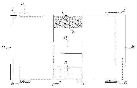
Figures 8 and 9 show an example of the dimensions (in inches) for the
10 lower ground plate 2, the positive plate 4, the negative plate 6 and the
upper
ground plate 8, including the dimensions of end portions 21, 41, 61 and 81,
end
portions 22, 42, 62 and 82, and bridges 23, 43, 63 and 83. With this 4-
conductorl3-insulator DC bus bar of Figures 8 and 9, an attenuation as high as
50 dB was obtained over a 3-dB cut-off frequency of 600 kHz.
Although the present invention has been described hereinabove by way
of preferred embodiments thereof, it can be modified at will within the scope
of
the appended claims, without departing from the spirit and nature of the
subject
invention.
As non limitative examples of such modifications, the bus bar may
comprise one or many pairs of conductor plates, the conductor plates can
present shapes other than rectangular, and the conductor plates and
electrically
insulating films do not need to be planar.